HARMON, JEFFREY LEE. 4H-SiC Trench-Gate MOSFET: Practical Surface-Channel Mobility Extraction (Under the direction of Dr. B. Jayant Baliga).
Silicon carbide (SiC) power MOSFET devices have the potential for a one-thousand times lower on-state resistance compared to silicon devices designed for the same blocking voltage, as defined by Baliga’s Figure of Merit. Analytical analysis of the SiC power MOSFET device reveals that the finite specific on-resistance of the MOSFET’s channel region becomes appreciable and dominant in power devices designed for lower blocking voltage ratings (e.g. 1200 V). Reduction of the specific on-resistance of the MOSFET’s channel region can be accomplished by reducing the cell pitch, increasing the effective carrier mobility in the channel, and/or increasing the capacitance of the gate-dielectric.
A trench-gate MOSFET design enables a substantially smaller cell pitch compared to the planar-gate MOSFET structure that currently dominates the commercial production market. Additionally, surface channel mobility on the alternative crystalline faces of a SiC trench-gate MOSFET is typically 2-3 times greater than channel mobility in planar-gate MOSFET structures. Combining the advantages of reduced pitch and increased channel mobility, the trench-gate MOSFET design provides a 44% reduction in on-state resistance from the historic planar-gate design.
of a specialized data extraction methodology for channel mobility in actual trench-gate MOSFET structures, 2) development of the fabrication process flow, tools, procedures, and process
specifications for manufacturing practical SiC MOSFET devices utilizing Research Triangle Nanotechnology Network laboratories, 3) original design of the trench-gate MOSFET structures and corresponding test structures with features critical to on-state performance equivalent to those in commercial state-of-the-art SiC power MOSFET devices, 4) fabrication of the SiC MOSFET devices and test structures, and 5) electrical characterization of fabricated devices and test structures.
No operational trench-gate MOSFETs were produced, attributed to capability limitations in available fabrication tools. The suspected root cause for the zero yield of trench-gate
MOSFET devices is a non-conformal aluminum gate metal deposition which is supported by the successful operation of the complementary planar-gate lateral MOSFET structures co-fabricated in this study. The fabrication process splits for high permittivity gate-oxide MOSFET devices were incomplete attributed to capability limitations of available fabrication process tools.
One hundred eighty eight inversion-mode planar-gate lateral MOSFET structures having a 40 nm thick gate-oxide (determined by C-V on co-fabricated N-MOS structures) grown by dry-thermal oxidation without a nitridation anneal, demonstrated an average surface-channel
effective mobility of 3.8 cm2/Vs. Using linear transmission line measurements, the N+
source/drain contact resistance was determined to be 2.2E-6 Ω-cm2 and the sheet resistance for the N+ SiC material was 1544 Ω/. P+ contacts were found to be non-conductive at potentials
+0.045 cm2/Vs per K over the temperature range 300 to 400°C which is consistent with an expected high density of interface trapped charge (re: lack of nitridation capability). Data obtained supports the theory that at elevated temperatures, trapped electrons are released producing a higher density of mobile channel electrons, proportional to the density of interface trapped charge. Determination of interface-state density on the fabricated devices was not possible because co-fabricated P-MOS capacitor test structures were non-functional (root cause is likely associated with the non-conductive P+ contacts).
by
Jeffrey Lee Harmon
A dissertation submitted to the Graduate Faculty of North Carolina State University
in partial fulfillment of the requirements for the degree of
Doctor of Philosophy
Electrical Engineering
Raleigh, North Carolina 2019
APPROVED BY:
_______________________________ _______________________________ Dr. B. Jayant Baliga Dr. Victor Veliadis
Chair of Advisory Committee
DEDICATION
This work is dedicated to the betterment of mankind and to the sustainable stewardship of the one earth that supports us all.
BIOGRAPHY
Jeffrey L. Harmon has demonstrated expertise in advancing wide bandgap semiconductor power device and photovoltaic technologies, two key elements of the global clean energy
economy, through experimental research, teaching, and voluntary educational activities, augmented with extensive manufacturing engineering and quality management experiences.
Jeff is currently a Research Scientist for the PowerAmerica Institute developing state-of-the-art silicon carbide semiconductor fabrication capabilities with the North Carolina State University Nanofabrication Facility team for pilot manufacturing SiC power devices.
Responsibilities include project planning, defining process sequencing and tooling requirements, developing standardized process block unit steps, assessing & maximizing line-edge control capabilities, and designing test structure devices for comprehensive process control and SiC power device product monitoring.
Since May 2014, Jeff has been pursuing his doctoral degree (graduation December 2019) for which he designed and fabricated customized SiC MOSFET devices utilizing capabilities in Research Triangle Nanotechnology Network (RTNN) laboratories including NCSU’s
Nanofabrication Facility (NNF), NCSU’s Analytical Instrumentation Facility (AIF), UNC’s
Chapel Hill Analytical and Nanofabrication Laboratory (CHANL), and Duke University’s Shared Materials Instrumentation Facility (SMIF).
Operating at 2000x Solar Concentrations at the Electronic Materials Conference in June 2012. Jeff has co-authored eight peer-reviewed publications and is an active member of IEEE.
Jeff’s earned a Master of Science degree in Electrical Engineering from North Carolina
State University in Raleigh in May 2012. Partially supporting his graduate education, Jeff invested eight semesters and four summer periods as a Teaching Assistant to educating our next generation of engineers, for which he received strong positive feedback, such as: “I am grateful for his help and not sure I would have passed the class without his help.”; “Don’t stop, the aid you provided was gamechanging.” ; “Thank you for all your help!” ; “He should teach the class.”; “Thanks Jeff!”; “Very helpful TA.” Jeff was nominated for NCSU’s Outstanding TA
Award in 2010.
Jeff was awarded a Graduate Assistance in Areas of National Need (GAANN)
Fellowship in Nanoscale Electronic and Energy Materials (NEEM) in 2011. Summer 2010, Jeff co-mentored a Research Experience Undergraduate (REU) student which culminated into an Engineering Grand Challenge winning poster in 2011 for Making Solar Energy Economical, awarded by the American Council of Engineering Companies (ACEC/NC) and Professional Engineers of North Carolina (PENC). Jeff created an original presentation, Energy &
Photovoltaics - The New Energy Era, which was presented to the IEEE student chapter at NCSU in 2010, and presented in 2009 & 2010 to the Young Scholars (YS), Research Experience for Teachers (RET), and Research Experience for Undergraduates (REU) programs for the Future Renewable Electric Energy Delivery and Management (FREEDM) Center, a National Science Foundation (NSF) Engineering Research Center (ERC).
Jeff’s acquired extensive manufacturing process engineering and quality management
accomplishments include over $946,000 in documented annual savings through improvements in safety, quality, productivity, delivery, and customer satisfaction while substantially reducing inventories and lead-times. Jeff’s experience also includes being a key engineer/manager in two new, “start-up” manufacturing facilities, and for a complete consolidation of one manufacturing
facility into another. Jeff has effectively implemented practical application of statistical methods (SPC/SQC, DoE) and Deming based quality programs (ISO-9001, QS- 9000, FMEA, PPAP, MSA) empowering associates to self-manage with fact-based decisions and was a Process Engineer for Milliken & Company when receiving the Malcolm Baldrige National Quality Award.
ACKNOWLEDGMENTS
I am grateful for the fantastic opportunity to conduct graduate research here at North Carolina State University. I am thankful to the Electrical & Computer Engineering Department for financial support via teaching assistantships. This work would not have been possible without funding from the PowerAmerica Institute and the U.S. Department of Energy.
I would like to express my gratitude to Dr. B. Jayant Baliga for his service as my Advisor & Committee Chair. I am especially grateful to Dr. Baliga for providing valuable time each week sharing his technical expertise in critical reviews and mentoring me through the doctoral process. I am also grateful for the many comprehensive and precisely detailed semiconductor power device physics books Dr. Baliga has published, which have also enabled me to gain an enormous amount of knowledge from his experiences.
I would like to thank Dr. Victor Veliadis, Dr. John Muth, and Dr. Veena Misra, my Graduate Committee Members for their time and support and Dr. Stephen Michielsen for his service representing NCSU’s Graduate School.
I am grateful for the Research Triangle Nanotechnology Network (RTNN) laboratories that made this experimental work possible including NCSU’s Nanofabrication Facility (NNF), NCSU’s Analytical Instrumentation Facility (AIF), UNC’s Chapel Hill Analytical and
TABLE OF CONTENTS
LIST OF TABLES ... xii
LIST OF FIGURES ... xiii
Chapter 1: Background & Motivations 1.1 Introduction ... 1
1.2 Silicon Power MOSFET and the Fundamental Tradeoff ... 2
1.3 Wide Band Gap Materials for Power Devices ... 5
1.4 4H-SiC Trench-Gate Power MOSFET ... 8
1.5 Crystal Orientation Impacts on Mobility ... 11
1.6 4H-SiC Trench MOSFET Specific On-Resistance & High-k Gate Dielectrics ... 17
1.7 References ... 22
Chapter 2: Physical Models for Mobility 2.1 Introduction ... 23
2.2 Physics of the MOS Capacitor ... 26
2.2.1 MOS Biasing Modes ... 27
2.2.2 The Ideal MOS Capacitor ... 30
2.2.3 Practical MOS capacitor - threshold voltage ... 35
2.2.4 MOS Capacitor Electric Field & Potential Distributions and Energy Band Diagram... 45
2.2.5 MOS Capacitance ... 47
2.3 Physics of MOSFET Device Mobility ... 48
2.3.1 The Conductivity Mobility Constant ... 49
2.3.2 Surface-Channel Mobility – Unique Scattering Mechanisms ... 51
2.3.3 Review of Empirical Surface-Channel Scattering Models ... 55
2.3.4 Channel Electron Quantum Confinement ... 60
2.3.5 Fowler-Nordheim Quantum Tunneling - Gate Oxide Leakage Current ... 64
Chapter 3: Mobility Study Experimental Design
3.1 Trench-Gate MOSFET Surface Channel Mobility Extraction Methodology ... 68
3.2 Simulated Predictions for Mobility Trial ... 73
3.3 Fabrication Device Design ... 74
3.4 Fabrication Mask Design ... 76
3.4.1 Photolithography ... 76
3.4.2 Contact Photolithography ... 76
3.4.3 Manual Alignment Markings ... 78
3.4.4 Mask Levels ... 79
3.4.5 Mask Polarity ... 80
3.4.6 Mask Delineation ... 81
3.4.7 Computer Aided Layout Design (CAD) ... 81
3.5 References ... 83
Chapter 4: Fabrication Process Design and Development 4.1 Introduction ... 84
4.1.1 Fabrication Process Sequence ... 84
4.1.2 Research Fabrication Process Development Effort Methodology ... 89
4.1.3 Unique Processing for Silicon Carbide ... 90
4.1.4 Fabrication Process Unit Step Development Efforts ... 91
4.1.5 Justification for Utilizing the NCSU-NNF ... 93
4.1.6 Four Gate-Oxide Formation Fabrication Process Splits ... 94
4.2 Fabrication Step 0: Wafer Material Design & Development... 97
4.2.1 Breakdown Optimization - Drift Region Design ... 98
4.3 Fabrication Step 1: “Zero” Etch Process Design & Development ... 100
4.4 Fabrication Step 2: Masking for P base Implantation Process Design & Development ... 103
4.4.1 1.4 µm SiO2 Mask Formation Process Design ... 105
4.4.2 Mask Formation Process Development ... 107
4.4.2.1 Stage 1: SiO2 deposition process development: (tool selection) ... 108
4.4.2.2 Stage 2: Densification process development of PECVD SiO2... 111
4.4.2.3 Stage 3: Photolithography process development of etching Mask ... 111
4.4.2.4 Stage 4a: Dry-etching silicon dioxide process development ... 113
4.4.2.4.1 Development of Unique Etch Process Metrology ... 114
4.4.2.4.3 Phenomenon Discovery and Theoretical Development
of the Robust Silicon Dioxide Etching Procedure ... 119
4.4.2.4.4 SiO2 Hard-Mask Dry-Etching Procedure... 126
4.4.2.5 Stage 4b: Wet-etching PECVD Silicon dioxide ... 127
4.4.2.6 Stage 5: Removal of photoresists and fluorocarbon residues ... 128
4.5 Fabrication Step 3: P Base Ion Implantation Process Design & Development ... 130
4.5.1 Introduction ... 130
4.5.2 P-Base Region Design ... 131
4.5.3 P Base Ion Implantation Process Design ... 135
4.5.4 P Base Implantation Process Development ... 137
4.6 Fabrication Steps 4 & 5: Masking and Ion implantation for N+ Source/Drain Process Design ... 138
4.6.1 Step 5: N+ Source and Drain Implantation Process Design ... 138
4.6.2 Step 4: N+ Source and Drain Ion Implantation Masking Process Design ... 139
4.7 Fabrication Steps 6 & 7: Masking and Ion implantation for P+ Contact Process Design ... 140
4.7.1 Step 7: P+ Contact Ion Implantation Process Design ... 140
4.7.2 Step 6: P+ Contact Ion Implantation Masking Process Design ... 141
4.8 Fabrication Step 8: High-Temperature Activation Anneal Process Design & Development ... 142
4.8.1 Carbon Capping Process Development ... 143
4.8.2 Packaging and Shipping ... 144
4.8.3 Carbon Cap removal Process Development ... 145
4.9 Fabrication Step 9: Trench Etching Process Design & Development ... 147
4.9.1 Introduction ... 147
4.9.2 SiC Trench Dry-Etching Process Design ... 147
4.9.3 SiC Trench Dry-Etching Process Development ... 151
4.9.3.1 Trial #1: ICP-RIE Dry-Etching SiC with SF6 and a Photoresist Mask ... 151
4.9.3.2 Trial #2: RIE Dry-Etching SiC with SF6 and a Silicon Dioxide Mask ... 156
4.9.3.3 Trial #3: ICP-RIE Dry-Etching SiC with SF6 and a Squared-wall Photoresist Mask ... 160
4.9.3.3.1 Spin coater spin speed process development trials ... 161
4.9.3.4 Mobility Study 4H-SiC device wafer dry-etching process & results . 162 4.10 Fabrication Step 10: Post Trench Dry-Etching Processing (Sacrificial Oxidation) Process Design & Development ... 164
4.12 Fabrication Step 12: Gate-Oxide Formation Process Design & Development ... 171
4.12.1 Process Split #1 – Dry Thermal Oxidation Gate-Oxide Process Design ... 171
4.12.2 Process Split #1 – Dry Thermal Oxidation Gate-Oxide Process Development ... 177
4.12.3 Process Split #2 – Deposited SiO2 Gate-Oxide Process Design & Development ... 181
4.12.4 Process Split #3 – Deposited High-k Dielectric Gate-Oxide Process Design ... 184
4.12.5 Process Split #4 – Deposited Silicon Nitride Gate-Oxide Process Design ... 185
4.13 Fabrication Steps 13, 14 and 15: Contact and Gate Formation Design & Development ... 186
4.13.1 Metallization Process Design ... 186
4.13.2 Fabrication Step #14 – Contact Metal Formation Process Design ... 188
4.13.3 Fabrication Step #15 – Gate and Probe Metal Formation Process Design ... 189
4.13.4 Metallization Process Development ... 190
4.13.5 Fabrication Step #14 Process Development for Process Splits #1 and #2 ... 191
4.13.6 Fabrication Step #14 Process Development for Process Split #3 ... 196
4.13.7 Fabrication Step #13 – Wet-etching Process Development ... 199
4.13.8 References ... 202
Chapter 5: Characterization and Experimental Results 5.1 Electrical Characterization ... 208
5.2 Experimental Results Summary for the Four Process Splits ... 210
5.3 Process Split #1 (dry thermal oxidation gate-oxide)... 211
5.3.1 Trench MOSFET Structures – Zero Yield ... 211
5.3.2 Contact Resistance Measurements (TLM) ... 212
5.3.3 MOS Capacitance Measurement Results ... 215
5.3.4 MOSFET Characterization ... 216
5.3.5 Planar-Gate MOSFET Measurement Data ... 218
5.3.6 Crystal Orientation and Planar MOSFET Channel Mobility ... 223
5.3.7 Channel Length Impacts on Planar MOSFET Devices ... 225
5.3.8 Temperature Impacts on Planar MOSFET Devices ... 229
5.4 Process Split #2 (ALD SiO2 gate-oxide) ... 237
5.4.1 Contact Resistance Measurements (TLM) ... 237
5.4.2 MOSFET Characterization: Suspect Root Causes for a Zero MOSFET Device Yield in Process Split #2 ... 238
Chapter 6: Future Work Recommendations
6.1 NO Nitridation Capability... 242
6.2 MOS Hall Effect Measurement Capability ... 242
6.3 Shielding Excessive Electric Fields in the 4H-SiC Trench MOSFET Gate-Oxide ... 243
6.4 Electric Fields in High-k Dielectrics... 247
6.5 Interface Engineering ... 249
6.6 Electric Field Profile with an Al2O3 Gate Dielectric ... 251
6.8 References ... 255
LIST OF TABLES
Table 1.1 Comparison of BFOM of Si and 4H-SiC for 1200V Device ... 6
Table 1.2 Specific on-resistance of 4H-SiC vertical 1200V planar-channel power MOSFET ... 8
Table 1.3 Specific on-resistance of 4H-SiC vertical 1200V trench power MOSFET ... 10
Table 1.4 Motivation for 4H-SiC trench MOSFET - Reduced specific on-resistance ... 10
Table 1.5 Advantages of high channel mobility in 4H-SiC 1200V trench MOSFET ... 17
Table 1.6 On-resistance of 4H-SiC 1200V trench MOSFET with higher channel mobility vs a planar-channel design ... 17
Table 1.7 Specific on-resistance of 4H-SiC vertical 1200V trench power MOSFET ... 18
Table 1.8 Impact of high-k dielectric on trench MOSFET specific on-resistance ... 20
Table 1.9 Impacts of high mobility & high-k dielectric on trench MOSFET specific on-resistance ... 21
Table 3.1 Layout design mask polarity selection ... 80
LIST OF FIGURES
Figure 1.1 Vertical power MOSFET schematic in blocking-mode with electric field
profile ... 2
Figure 1.2 Silicon’s fundamental tradeoff curve for power devices ... 4
Figure 1.3 Fundamental tradeoff curve for power devices ... 6
Figure 1.4 4H-SiC vertical power MOSFET with current path highlighted ... 8
Figure 1.5 Motivations for the trench-gate power MOSFET ... 9
Figure 1.6 4H-SiC vertical power trench-gate MOSFET with current path highlighted ... 10
Figure 1.7 a) 4H-SiC (0001) wafer - crystal orientation, b) Cross-sectional view of basal (0001) plane in hexagonal crystal structure ... 11
Figure 1.8 4H-SiC vertical power trench-gate MOSFET with current path highlighted ... 18
Figure 1.9 Gate-oxide relative permittivity impact on specific channel resistance on trench MOSFET ... 20
Figure 2.1 4H-SiC bulk electron mobilities (model details described in text) ... 25
Figure 2.2 Bulk electron mobility as a function of temperature for the 4H-SiC p-type base region of the mobility study ... 26
Figure 2.3 Energy band diagram of 4H-SiC MOS capacitor at strong-inversion ... 30
Figure 2.4 Semiconductor charges as a function of surface potential ... 32
Figure 2.5 4H-SiC inversion-mode MOS threshold voltage for varying Qit ... 42
Figure 2.6 Semiconductor charges and interface trapped charge (Qit) as a function of surface potential ... 43
Figure 2.7 Effective electric field versus gate bias (with and without Qit) ... 45
Figure 2.8 MOS Electric Field Distribution ... 46
Figure 2.9 MOS Potential Distribution ... 46
Figure 2.11 Actual MOS capacitance as a function of actual MOS gate bias ... 48
Figure 2.12 6H-SiC electron surface mobility with surface coulombic scattering ... 56
Figure 2.13 4H-SiC surface electron mobility scattering components & cumulative impact ... 57
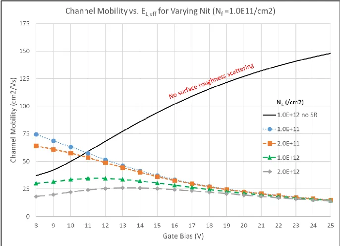
Figure 2.14 4H-SiC surface electron mobility for varying interface trapped charge densities... 59
Figure 2.15 4H-SiC (0001) surface electron mobility for varying interface trapped dharge densities with and without surface roughness scattering ... 59
Figure 2.16 Quantum confinement effects - conduction band energy level increase at threshold voltage ... 61
Figure 2.17 Quantum confinement effects for gate biases above threshold ... 62
Figure 2.18 4H-SiC energy band diagram showing triangular barrier at threshold voltage ... 64
Figure 2.19 4H-SiC energy band diagram showing triangular barrier at a gate voltage of 15 V ... 65
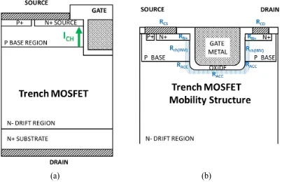
Figure 3.1 Very long channel MOSFET or “FatFET” for measuring channel mobility ... 68
Figure 3.2 (a) Trench MOSFET schematic showing channel is vertically orientated. (b) Unique structure for extracting trench MOSFET channel mobility ... 69
Figure 3.3 Mobility study trench-gate and planar-gate MOSFET structures ... 70
Figure 3.4 Mobility study trench-gate MOSFET data extraction method. ... 71
Figure 3.5 Mobility study planar-gate MOSFET data extraction method ... 72
Figure 3.6 Overhead view of trench and planar MOSFET structures ... 74
Figure 3.7 Trench MOSFET structure schematic with critical pattern edges itemized ... 78
Figure 3.8 Complete mask layout... 82
Figure 3.9 Die layout over a 100mm wafer... 82
Figure 4.2 Gate-oxide permittivity impact on specific channel resistance in the
trench-gate MOSFET ... 95
Figure 4.3 Punch-through breakdown potential as a function of N- drift region doping ... 98
Figure 4.4 On-resistance as function of breakdown voltage. N-drift region design chosen to be 10 µm thickness and 8.E15/cm3 n-type doping ... 99
Figure 4.5 Possible materials for masking the P base ion implantation process ... 103
Figure 4.6 Al ion penetration into the SiO2 masking material ... 105
Figure 4.7 Cracking/flaking after densification for TEOS SiO2 PECVD from NCSU-NNF... 109
Figure 4.8 Uneven SiO2 deposition from Duke-SMIF PECVD tool; image taken prior to unloading ... 109
Figure 4.9 Metal coins that had been previosuly used as wafer stops inside Duke- SMIF PECVD ... 109
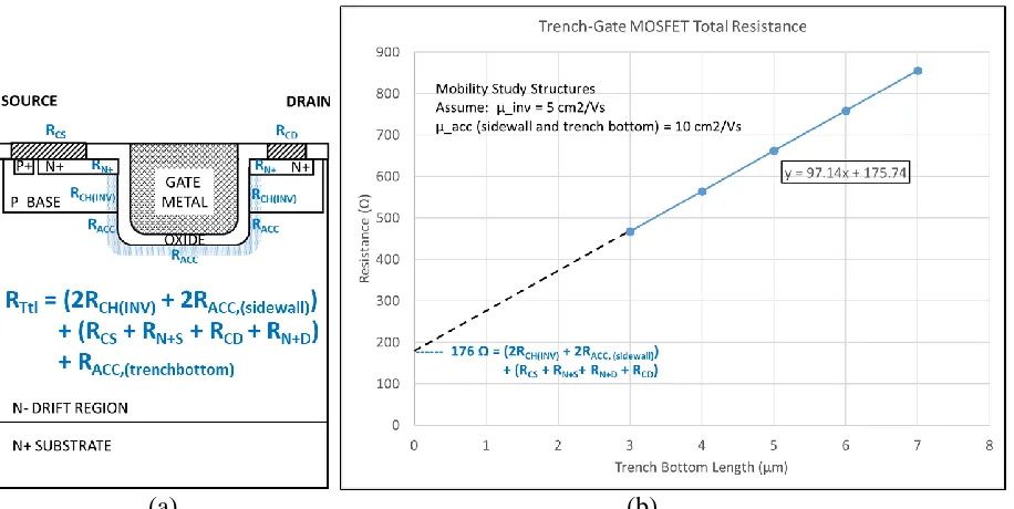
Figure 4.10 Two-dimensional current density profile in 4H-SiC trench MOSFET structure in blocking mode ... 132
Figure 4.11 Impact of P-base region thickness on reach-through condition in trench MOSFET structure for 1E17/cm3 p-type doping ... 133
Figure 4.12 P base reach-through caused breakdown ... 134
Figure 4.13 Two-dimensional current density profile for additional simulations ... 135
Figure 4.14 Predicted Al ion profile in the 4H-SiC mobility study’s P base regions ... 136
Figure 4.15 Close-up of P base implantation schedule near the 4H-SiC wafer’s surface ... 137
Figure 4.16 Nitrogen ion implantation schedule for N+ source and drain regions ... 138
Figure 4.17 Nitrogen ion penetration into the silicon dioxide masking material ... 139
Figure 4.18 Aluminum ion implantation schedule for the P+ contact region ... 140
Figure 4.19 Aluminum ion penetration into the silicon dioxide masking material for P+ contact ... 141
Figure 4.21 Trial #1 dry-etched SiC trench SEM images (NCSU-AIF FEI Quanta
3D FEG) ... 152 Figure 4.22 Trial #1 sidewall striations and contamination (NCSU-AIF Hitachi
S3200N SEM) ... 153 Figure 4.23 Verios SEM images of Trial #1 trench sidewall roughness (assumed to
be carbon)... 154 Figure 4.24 Trial #2 dry-etched SiC trench SEM image (NCSU-AIF FEI Quanta
3D FEG) ... 157 Figure 4.25 Trial #2 dry-etched SiC trench cross-section (NCSU-AIF FEI Quanta
3D FEG) ... 158 Figure 4.26 4H-SiC modeled dry-thermal oxidation curves for sacrificial oxidation
process run ... 166 Figure 4.27 Purchased saw blade: ZH05‐SD4000‐N1‐50 ... 167 Figure 4.28 Oxide thickness data on Si wafers in the sacrificial oxide thermal growth
process run ... 178 Figure 4.29 Modeled Si oxidation curves and actual process data ... 179 Figure 4.30 4H-SiC modeled oxidation thickness curves ... 180 Figure 4.31 The crucible liner’s position after jumping out of the hearth pocket.
Image taken upon opening the NCSU-NNF 6” E-beam Evaporator ... 197 Figure 4.32 Glassy coated graphite crucible liner containinng Al metal and broken at
the beginning of the initial deposition run ... 197 Figure 4.33 Hearth inside the NCSU-NNF 6” E-beam chamber after removing the
broken crucible liner with Al metal ... 198 Figure 5.1 Mobility Study Fabrication Process Split #1 quarter wafer under test on
the PowerAmerica Power Device Electrical Characterization Station ... 208 Figure 5.2 PowerAmerica’s Semiconductor Power Device Electrical Characterization
Station managed by B. Jayant Baliga ... 209 Figure 5.3 Signatone probing station microscopic image of probe tips, with Kelvin
configuration on source and drain, set on a mobility study trench-gate
Figure 5.4 Process Split #1 N+ source/drain contacts demonstrate excellent ohmic
Behavior ... 213
Figure 5.5 Process Spilt #1 TLM results for N+ contact resistance determination ... 214
Figure 5.6 Process Split #1 P+ contacts demonstrate an infinite resistance (i.e. no contact) ... 214
Figure 5.7 Process Split #1 N-MOS capacitance for determining thickness of gate Oxide ... 216
Figure 5.8 Mobility study device quarter wafer in testing on PowerAmerica’s Power Device Electrical Characterization Station ... 217
Figure 5.9 Example of Id-Vg (at Vd = 100mV) curve captured for VTH analysis. The quasi-linear region is highlighted in orange and the linear extraction method for VTH is shown ... 219
Figure 5.10 Histogram of threshold voltage values for planar MOSFETs in Process Split #1 ... 219
Figure 5.11 Measured MOSFET transfer curve set ... 220
Figure 5.12 Linear region’s slope determination from measured data for use in effective mobility calculations ... 221
Figure 5.13 Histogram of effective mobility values for planar MOSFETs in Process Split #1 ... 222
Figure 5.14 Orientation angle impact on measured threshold voltage ... 223
Figure 5.15 Orientation angle impact on measured resistance ... 224
Figure 5.16 Orientation angle impact on measured effective mobility ... 224
Figure 5.17 Channel length impact on measured threshold voltage ... 225
Figure 5.18 Channel length impact on measured resistance data ... 226
Figure 5.19 Channel length impact on measured resistance box chart ... 227
Figure 5.20 Magnitude of channel length impact on measured resistance ... 227
Figure 5.21 Channel length impact on measured effective mobility ... 228
Figure 5.23 Planar MOSFET threshold voltage measured with variation in temperature .... 230 Figure 5.24 Analytical 4H-SiC threshold voltage variation with temperature... 231 Figure 5.25 Planar-gate MOSFET measured resistance variation with temperature ... 232 Figure 5.26 Planar MOSFET measured effective mobility variation with temperature ... 233 Figure 5.27 Analytical 4H-SiC intrinsic carrier concentration with temperature ... 235 Figure 5.28 Process Split #2 N+ source/drain contacts demonstrate excellent ohmic
Behavior ... 237 Figure 5.29 Process Spilt #2 TLM results for N+ contact resistance determination ... 238 Figure 6.1 Trench-gate MOSFET and electric field profile in blocking mode ... 244 Figure 6.2 Simulated schematic and specifications for P+ shielding “pinch” structure
in a 4H-SiC trench MOSFET ... 245 Figure 6.3 P+ barrier depth simulation results ... 246 Figure 6.4 P+ trench bottom shielding simulation results ... 246 Figure 6.5 Simulated schematic and specifications for evaluation of high-k dielectrics .... 248 Figure 6.6 Simulated electric fields at breakdown in trench MOSFET when limited
by the avalanche condition in the 4H-SiC ... 248 Figure 6.7 Simulated electric fields at breakdown in a trench MOSFET when limited
by the electric field in the dielectric reaching 3 MV/cm ... 249 Figure 6.8 Simulated schematic for the MOS structure at the bottom of the trench
in a trench-gate MOSFET structure ... 252 Figure 6.9 Simulated electric field profile for an Al2O3 gate dielectric with a 1.5 nm
SiO2 interfacial layer (insert includes drift region) ... 252 Figure A.1 E-beam gun housing assembly – electrical connections and e-gun
CHAPTER 1
Background & Motivations
1.1 Introduction
Converting electricity for efficient transport and consumption has been an on-going engineering challenge throughout our history. In 1886, the Westinghouse Electric Company demonstrated the advantages of power conversion by using transformers to step-up AC voltage for transmission and again to step down AC voltage for the end use in incandescent lighting. This AC power delivery system proved to have very little transmission power losses and formed the basis for today’s U.S. electric power transmission system.
Converting electric power using semiconductor power devices began following the invention of the transistor in 1947 by John Bardeen, Walter Brattain, and William Shockley. In the 1950’s, semiconductor thyristors began replacing vacuum tubes in power conversion systems
and the power device evolution ensued. In the 1960’s, came development of gate-controlled switches such as the gate turn-off (GTO) thyristor. In the 1970’s, manufacturing of power silicon metal-oxide-semiconductor field-effect transistor (MOSFET) devices became possible with the evolution of the integrated circuit industry, including utilization of CMOS
1.2 Silicon Power MOSFET and the Fundamental Tradeoff
A Si power MOSFET is 1) a voltage-controlled gated device with high input impedance enabling simple gate drive circuitry, 2) a unipolar or majority carrier device enabling very fast switching void of adverse reverse recovery issues found with bipolar designs, and 3) capable of bidirectional current flow by either using gated synchronous rectification or through the internal body diode which includes a ~0.7 V turn-on voltage drop.
A schematic of a vertical power MOSFET in blocking mode with the electric field profile (assuming constant doping concentration) is shown in Figure 1.1. The blocking voltage potential (BV) is equal to the integral of the electric field over the N- drift region (neglecting the small blocking potential supported inside P base region). BV is dependent on the magnitude of the critical electric field, ℇc (electric field at onset of the avalanche breakdown phenomenon) and the
depletion width, Wd into the N- drift region.
Figure 1.1: Vertical power MOSFET schematic in blocking-mode with electric field profile.
By integrating Poisson’s equation (Equation 1.1) over the drift region, and assuming the
relationship between the drift region’s doping concentration, Nd, and the drift region’s depletion
width can be determined (Equation 1.2).
𝑑ℇ(𝑥)
𝑑𝑥 =
𝑞
𝜖𝑠(𝑝 − 𝑛 + 𝑁𝑑
+− 𝑁
𝑎−) Equ. 1.1
𝑊𝑑 =𝜖𝑠ℇ𝑐
𝑞𝑁𝑑 Equ. 1.2
Combining Equation 1.2 with the geometry in Figure 1.1, the relationship between the blocking potential and the drift region’s doping concentration is determined (Equation 1.3).
𝐵𝑉 = 𝜖𝑠ℇ𝑐2
2𝑞𝑁𝑑 Equ. 1.3
These relationships show that a designer can reduce the doping concentration of the N- drift region for a proportional increase blocking voltage potential at the cost of proportionally increasing the N- drift region’s layer thickness (to account for the proportional increase in depletion width). It needs to be noted that the critical electric field is also dependent on doping concentration. However, this relationship is very weak as the critical electric field increases by about a factor of two for a three order of magnitude reduction in doping concentration.
𝑅𝑜𝑛,𝑖𝑑𝑒𝑎𝑙 = 𝑊𝑑 𝑞𝜇𝑛𝑁𝑑 =
𝜖𝑠ℇ𝑐 𝑞2𝜇
𝑛𝑁𝑑2
Equ. 1.4
The minimum or ideal specific on-resistance, Ron,ideal (in Ω-cm2) for a power MOSFET is
assumed to be equal to the drift region’s specific resistance, Rd,ideal, which is determined by the
depletion width over the conductivity for the N- drift region (Equation 1.4). The combined effects from a reduction in the N- drift region’s doping concentration results in a quadratic increase in Ron,ideal; thus, at larger blocking voltages, Ron,ideal quickly becomes prohibitively large
power MOSFET devices to low voltage (< ~150V) applications (Figure 1.2). With high-frequency switching capability, Si MOSFETs are well suited for switch-mode power supplies.
Figure 1.2: Silicon’s fundamental tradeoff curve for power devices.
The insulated gate bipolar transistor (IGBT) was commercially introduced in the early 1980’s and created new market opportunities for power devices in medium and high voltage
applications. In the IGBT structure, carrier injection provides conductivity modulation to the drift region decoupling the operational drift region resistance from its doping concentration. This design freedom enables lowing the drift region’s doping concentration for much higher
blocking potentials without severely compromising on-resistance. However, conductivity modulation comes with the price of a slower switching speed capability and markedly increased reverse recovery energy losses during the switching off transient.
The super-junction (SJ) MOSFET entered the semiconductor power device market in the early 2000’s. Charge-coupled power device designs, which include the SJ-MOSFET,
circumvent the fundamental tradeoff limitation by decoupling the drift region’s doping
concentration from device’s blocking capability. This allows the design freedom to drastically
high-frequency switching capability of unipolar devices with extremely low on-resistances, superjunction power MOSFETs offer sufficient benefits for market penetration into medium-voltage, high-frequency applications. However, wide-spread adoption of the SJ-MOSFETs have been hindered by the radically increased manufacturing complexity for this unique design.
1.3 Wide Band Gap Materials for Power Devices
By solving Equation 1.3 for Nd and substituting into Equation 1.4 produces Equation 1.5,
an alternative form for Ron,ideal. The denominator of Equation 1.5 depends only on the material’s
properties and is defined as Baliga’s figure of merit for semiconductor power devices
(BFOM)[1]. Thus, the physics governing the tradeoff between blocking potential capability and on-state specific resistance in MOSFETs are constrained by silicon’s material properties.
𝑅𝑜𝑛,𝑖𝑑𝑒𝑎𝑙 = 4𝐵𝑉2
𝜖𝑠𝜇𝑛ℇ𝑐3 Equ. 1.5
According to the BFOM, wide band gap materials such as silicon carbide (SiC) or gallium nitride (GaN) enable superior power devices compared to silicon materials, by drastically shifting the fundamental tradeoff curve (see Figure 1.3). This performance improvement is obtained via the wide band gap material’s ability to support higher critical
1200V 4H-SiC MOSFET device with an operational Ron equivalent to that in a 100V Si MOSFET (Figure 1.3).
Table 1.1: Comparison of BFOM of Si and 4H-SiC for 1200V Device.
Figure 1.3: Fundamental tradeoff curve for power devices.
The first demonstration of power devices in silicon carbide material were Schottky barrier rectifiers in 1992 [2]. Commercially produced SiC power MOSFET devices were introduced into the market in 2011 [3]. GaN substrate material does not yet meet the quality necessary for producing cost-competitive, vertical power devices such as MOSFETs, thus power devices fabricated in GaN materials are currently limited to planar HEMT devices taking
new tooling is reduced to only the advanced processes necessary for silicon carbide manufacturing (e.g. heated ion implantation and high-temperature activation annealing).
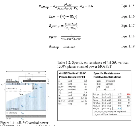
Analytical physical modeling of the specific resistances in a 4H-SiC vertical planar-gate power MOSFET device was performed using Equations 1.6 through 1.19 developed following references [1] & [4]. The planar-gate structure is shown in Figure 1.4 noting that no P+ contacts are shown as these are contacted though Vias orthogonal to this cross section. The analysis shows that resistance of the short, 0.6 µm channel dominates all other resistances accounting for 43% of the total specific on-resistance (Table 1.2). The second largest contributor, accounting for 35% of the total specific resistance, is the drift region which is set by the desired blocking voltage potential, as previously stated. The substrate, which is assumed to be thinned to down to 200 µm for minimizing this unavoidable contributor in all vertical SiC devices, is the third largest contributor accounting for 15% of the total.
𝑅𝑂𝑁,𝑠𝑝= 𝑅𝐶𝐻,𝑠𝑝+ 𝑅𝐷,𝑠𝑝+ 𝑅𝐴𝐶𝐶,𝑠𝑝+ 𝑅𝐽𝐹𝐸𝑇,𝑠𝑝+ 𝑅𝑠𝑢𝑏,𝑠𝑝 Equ. 1.6
𝑅𝐶𝐻,𝑠𝑝 = 𝑝𝐿𝑐ℎ
𝜇𝑛,𝑖𝑛𝑣𝐶𝑜𝑥(𝑉𝑔−𝑉𝑇) Equ. 1.7
𝐶𝑜𝑥 = 𝜖𝑜𝑥
𝑡𝑜𝑥 Equ. 1.8
𝑅𝐷,𝑠𝑝 = 𝑅𝐷1,𝑠𝑝 + 𝑅𝐷2,𝑠𝑝 Equ. 1.9
𝑅𝐷1,𝑠𝑝 = 𝜌𝐷𝑝𝑙𝑛 ( 𝑝
𝑊𝐽−𝑊0,𝐽) Equ. 1.10
𝑅𝐷2,𝑠𝑝 = 𝜌𝐷(𝑡𝐷− 𝑝 + 𝑊𝐽− 𝑊0,𝐽− 𝑥𝐽,𝑃− 𝑊0,𝐷) Equ. 1.11
𝜌𝐷 = 1
𝑞𝜇𝑛,𝑑𝑟𝑖𝑓𝑡𝑁𝑑 Equ. 1.12
𝑊0 = [2𝜖𝑠𝑉𝑏𝑖 𝑞𝑁𝑑 ] 1 2 ⁄ Equ. 1.13 𝑉𝑏𝑖 = 𝑘𝑇 𝑞 𝑙𝑛 ( 𝑁𝑎𝑁𝑑
𝑅𝐴𝐶𝐶,𝑠𝑝 = 𝐾𝐴 𝑝𝐿𝐴𝐶𝐶
𝜇𝑛,𝑎𝑐𝑐𝐶𝑜𝑥(𝑉𝑔−𝑉𝑇), 𝐾𝐴 = 0.6 Equ. 1.15
𝐿𝐴𝐶𝐶 = (𝑊𝐽− 𝑊0,𝐽) Equ. 1.16
𝑅𝐽𝐹𝐸𝑇,𝑠𝑝 =
𝜌𝐽𝐹𝐸𝑇𝑥𝑗𝑝𝑝
(𝑊𝐽−𝑊0,𝐽) Equ. 1.17
𝜌𝐽𝐹𝐸𝑇 =
1
𝑞𝜇𝑛,𝐽𝐹𝐸𝑇𝑁𝑑,𝐽𝐹𝐸𝑇 Equ. 1.18
𝑅𝑠𝑢𝑏,𝑠𝑝 = 𝜌𝑠𝑢𝑏𝑡𝑠𝑢𝑏 Equ. 1.19
Table 1.2: Specific on-resistance of 4H-SiC vertical 1200V planar-channel power MOSFET
Figure 1.4: 4H-SiC vertical power MOSFET with current path highlighted.
1.4 4H-SiC Trench-Gate Power MOSFET
area-based, specific on-resistance. Additionally, the trench-gate MOSFET design eliminates the JFET region.
Figure 1.5: Motivations for the trench-gate power MOSFET
Analytical mathematical modeling of resistances in the 4H-SiC trench-gate power MOSFET design shown in Figure 1.6 was performed using Equations 1.20 through 1.23 following references [1] & [4] with Equations 1.7, 1.8, 1.9, 1.12, 1.15, and 1.19. In Tables 1.3 and 1.4, this analysis shows that with the increased channel density and elimination of JFET region, the 1200V 4H-SiC trench-gate power MOSFET design has a 2.08 mΩ-cm2 total specific on-resistance, which is 24% smaller than the 2.75 mΩ-cm2 specific on-resistance for the planar-channel MOSFET design.
𝑅𝑂𝑁,𝑠𝑝= 𝑅𝐶𝐻,𝑠𝑝+ 𝑅𝐷,𝑠𝑝+ 𝑅𝐴𝐶𝐶,𝑠𝑝+ 𝑅𝑠𝑢𝑏,𝑠𝑝 Equ. 1.20
𝑅𝐷1,𝑠𝑝 = 𝜌𝐷𝑝𝑙𝑛 (2𝑝
𝑊𝑇) Equ. 1.21
𝑅𝐷2,𝑠𝑝 = 𝜌𝐷(𝑡𝐷− 𝑝 + 𝑊𝑡
𝐿𝐴𝐶𝐶 = (𝑡𝑇− 𝑥𝑗𝑝) Equ. 1.23
Table 1.3: Specific on-resistance of 4H-SiC vertical 1200V trench-gate power MOSFET.
Figure 1.6: 4H-SiC vertical power trench-gate MOSFET with current path highlighted.
Table 1.4: Motivation for 4H-SiC trench-gate MOSFET - Reduced specific on-resistance.
In today’s state-of-the-art 4H-SiC power MOSFETs, the channel current flows in the
sufficiently high for enabling market acceptance. However, there is still great potential for improvement towards the bulk electron mobility of ~700 cm2/Vs (at 1E17/cm3 doping). Improving the 4H-SiC MOSFET surface channel mobility is an on-going effort [5].
1.5 Crystal Orientation Impact on Mobility 4H-SiC Bulk Anisotropic Mobility.
The SiC hexagonal crystalline structure has been shown to demonstrate anisotropic bulk carrier mobilities. In traditional practical 4H-SiC MOSFET structures, the channel runs along the wafer’s surface or the (0001) plane. In 1994, Schaffer et al. demonstrated that along the
Si-face or (0001) plane, bulk carrier mobilities were isotropic[6]. Orthogonal to the (0001) plane, mobilities along the a-face and m-face planes are 20% higher compared to along the (0001) plane and this ratio is temperature independent.
a) b)
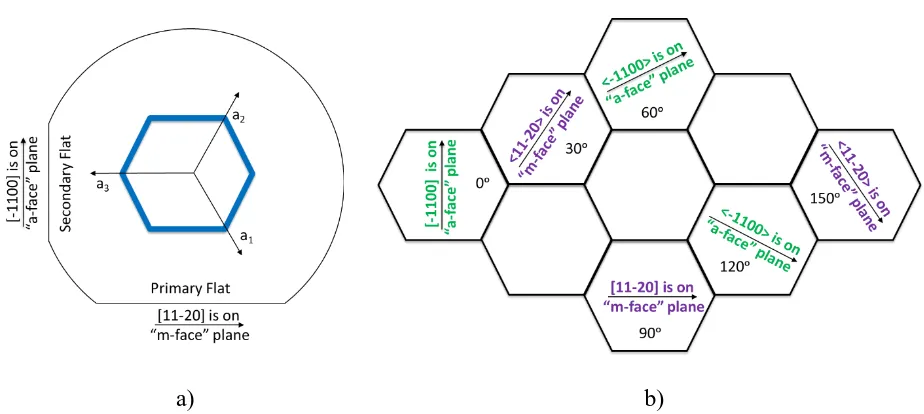
Figure 1.7: a) 4H-SiC (0001) wafer - crystal orientation,
b) Cross-sectional view of basal (0001) plane in hexagonal crystal structure.
4H-SiC Crystalline Structure.
For this research study, a (0001) orientation 4H-SiC wafer, cut off-axis 4° towards <1120> was used. Orientation of 4H-SiC’s hexagonal crystalline structure to the process wafer is shown in Figure 1.7. In this research study, crystal planes are denoted inside brackets with Bravais-Miller indices having the form of ( hkil ) where i = -h-k, and l = the c-plane, normal to plane of page. Crystal directions are normal to planes and denoted with square-brackets with the equivalent family of crystal directions denoted inside angled brackets (i.e. < >).
Published Anisotropic SiC Channel Mobility Research
A study of 4H-SiC inversion-mode surface-channel mobilities comparing the Si-face (0001) and a-face (11-20) planes demonstrated a positive temperature dependency for peak mobility on the Si-face and a negative temperature dependency for peak mobility on the a-face indicating different scattering mechanisms were dominant[7]. Noteworthy is that the inversion-mode, surface-channel mobility on the a-face peaked at 80 cm2/Vs, substantially greater than the
33 cm2/Vs peak mobility for Si-face 4H-SiC. However, practical devices are typically operated at gate biases ~15-20 V for ensuring stable device operation which is an order of magnitude greater than the 1 to 2 V gate bias where these peak-mobility values occurred. Additionally, practical power MOSFETs typically have P Base doping concentrations in the upper 1016/cm3 to 1017/cm3 range, which is about two orders of magnitude greater than the doping used for this
Ariyoshi et al. completed a study measuring surface-channel mobility in two directions on each of the three crystal planes relevant to the hexagonal crystal structure in order to evaluate the mobility anisotropy on each plane. This study included both accumulation-mode and
inversion-mode channel designs over a range of gate biases[8]. Along the 4H-SiC (0001) crystal surface, mobility was found to be isotropic. The (0001) inversion-mode field-effect mobility was ~25 cm2/Vs at gate bias of 20V, a typical operational gate voltage on practical devices. At a 20V gate bias, the inversion-mode surface-channel mobility, orthogonal to the (0001) plane, was ~75 cm2/Vs for both the a-face and m-face planes, which is triple the mobility value on the (0001) plane. Slight inversion-mode surface-channel mobility anisotropy on the a-face and m-face planes was present, exhibiting ~5 cm2/Vs difference with the [11-20] direction being greater than the [0001] direction on both crystal planes.
Comparing the accumulation-mode and inversion-mode designs, it is noteworthy to state that for a wide range of biases surrounding the typical practical gate bias of 20V, the surface-channel mobility is identical in both operational modes; this aspect is consistent with having one mobility degradation mechanism being commonly dominant and independent of the channel operational mode. However, the profile of mobility versus gate bias is starkly different between accumulation-mode and inversion-mode at low gates biases which is likely attributed different physics governing development of the MOS channel carrier density with gate bias. Typical of “normally-on” transistor behavior, profiles for the accumulation-mode devices at gate biases
the accumulation-mode peak-mobility likely forbids exploiting its advantages in practical applications.
The inversion-mode MOSFET’s P-base doping level in this study was an order of magnitude lower than in practical devices. Like the previous reference, devices in this study were planar-channel MOSFETs fabricated on wafers cut on different crystal orientations, so practical impacts from etching during fabrication of trench-gate MOSFETs were not captured in the results. It is noteworthy to include that the gate-oxide for this study was a deposited high-temperature oxide (HTO) followed by NO post-oxidation anneal. A set of additional samples were studied where the gate-oxide was thermally grown with pyrogenic steam followed by an H2
post-oxidation anneal and the relative anisotropic behavior was identical (although absolute values differed).
Impact of Interface Trapped Charge Density on Channel Mobility.
One primary area of focus for practical SiC MOSFETs surrounds correlating mobility degradation with the interface trapped charge density (Qit in C/cm2, Dit in #/cm2/eV, or Nit in
#/cm2) which in SiC is well known to be at least an order of magnitude greater than that in comparable silicon MOSFETs. Nakazawa et al. developed an improved method for
characterizing Nit during research evaluating the impact of interface trapped charge density on
surface-channel mobility degradation. They showed that effective mobility correlated well with interface trapped charge determined with their “C-φ” method, demonstrating a slope equal to -1.
In their findings, the (0001) crystal plane has markedly higher Nit values and simultaneously
plane. An interesting discovery is that with the C-φ method, fast states are accurately captured enabling measurement of the nitrided interface trapped charge density. “The high channel mobilities for (11¯20) and (1¯100) MOSFETs can be correlated with the lower density of fast interface states generated by nitridation”[9]. Devices in this study were also planar-channel MOSFETs fabricated on wafers cut on different crystal orientations; thus practical impacts from trench etching were not captured in the results. Samples were prepared via dry-oxidation followed by NO post-oxidation anneal.
Published Experiments with Practical Etching.
Ariyoshi et al. measured the mobility anisotropy between the a-face and m-face planes on sidewalls of trenches etched into a (0001) 4H-SiC wafer with trenches orientated every 15° of rotation[10]. For the 4H-SiC hexagonal structure, the crystal becomes crystallographically identical every 60° of rotation; thus one would expect mobility data values to repeat at that interval. Samples were prepared with a deposited high-temperature gate-oxide followed by one of three post-oxidation anneal (POA) process variations. It was found that for samples with a wet-oxidation and H2 POA, data trended cyclically lower with rotation from 0° to 180° with
local maximums corresponding to a-face planes and local minimums corresponding with m-face planes; a-face data trended from 40 cm2/Vs to 26 cm2/Vs. For samples prepared using an
ammonia and N2O POA, data trended lower linearly (no local maximums or minimums) from 28
to 20 cm2/Vs. For the N2O POA, data likewise linearly trended lower from 15 to 10 cm2/Vs. It
Practical Angles from Off-cut Wafers and Etching.
Work by Yano et al. found that the 8° off-axis cut wafer and a practical 5° slant from etching produced one sidewall with an estimated 3° off-plane in the [0001] direction with the opposite sidewall being 13° off-plane[11]. To confirm this aspect, a portion of this study was reproduced using an on-axis (zero offcut angle) wafer and an etching process more capable of producing vertical sidewalls; thus, the practical sidewalls were expected to be exactly on-plane in the [0001] direction[12]. Mobility improved to 71 and 66 cm2/Vs from 43 and 21 cm2/Vs for (11-20) and (-1-120) planes, respectively. Note that these mobility values on practically etched wafers are very close to the mobility values produced by authors using wafers cut on alternative crystal axes. Thus, the surface-channel mobility in practical trench-gate MOSFETs may be substantially higher than in planar-gate structures.
In conclusion, crystal orientation has been shown to have a strong influence on surface-channel mobility where the 4H-SiC a-face and m-face crystal planes have demonstrated superior mobilities values compared to the (0001) surface channel plane in traditional 4H-SiC MOSFETs. Combining the off-cutting of wafers which is necessary for epitaxial growth, and the
non-perfectly vertical sidewalls from practical trench etching, obtaining perfect crystal orientation of surface channels will likely be very difficult to consistently accomplish in practical 4H-SiC trench-gate MOSFETs. For the mobility study, planar-gate and trench-gate MOSFET samples were orientated at 15° orientations from 0° to 90° from the 4H-SiC wafer’s flat edge in order to capture orientation impacts.
interdependent impacts from the practical trench etching processes; it is reasonable to assume that practical trench etching would have some negative impacts on surface channel mobility.
Assuming a practical the realization of 50 cm2/Vs for the surface channel mobility in a trench-gate MOSFET equates to a 70% reduction in the channel region’s specific on-resistance (Table 1.5). Combining the benefits of the trench-gate design with an increased mobility equates to a 44% reduction in specific on-state resistance compared to the benchmark, vertical planar-channel MOSFET design (Table 1.6).
Table 1.5: Advantages of high channel Table 1.6: On-resistance of 4H-SiC 1200V mobility in 4H-SiC 1200V trench-gate trench-gate MOSFET with higher channel MOSFET. mobility vs a planar-gate design.
This research effort is to experiementally evaluate channel mobility on the vertical channels of 4H-SiC trench-gate MOSFET structures with comparison to co-fabricated 4H-SiC planar-gate MOSFET designs.
inversion channel mobility is assumed equal to that of state-of-the-art planar-gate MOSFET devices without consideration of the potential mobility advantages on the alternative crystal faces of the trench-gate MOSFET structure). The channel resistance at 0.81 mΩ-cm2 accounts for 38% of the total device specific on-resistance of 2.13 mΩ-cm2. The other two major contributing
resistances, the drift region and substrate, are essentially fixed and cannot easily be improved; thus, the channel region is the prime opportunity for improving the 1200V trench-gate
MOSFET’s specific on-resistance.
Table 1.7: Specific on-resistance of 4H-SiC vertical 1200V trench-gate power MOSFET.
Figure 1.8: 4H-SiC vertical power trench- gate MOSFET with current path highlighted.
In review of Equation 1.24, options for reducing the channel region’s specific on-resistance include: 1) reducing the channel length, 2) reducing the pitch, 3) increasing the
increased by increasing the permittivity and/or by reducing the thickness. Therefore, replacing the silicon dioxide gate-oxide material with an equivalent thickness of dielectric material having a higher relative permittivity will directly result in a reduction of the MOSFET’s total specific
on-resistance. The high-k allows the gate dielectric to contribute a higher capacitance for a given thickness; thus, the channel’s carrier density (sheet charge density) increases for a given gate bias. Assuming no impacts on the mobility, a higher relative permittivity gate dielectric results in a lower channel resistance by increasing the free electron density in the channel at a given gate bias.
𝑅𝐶𝐻,𝑠𝑝 = 𝐿𝑐ℎ𝑝
𝜇𝑛,𝑖𝑛𝑣𝐶𝑜𝑥(𝑉𝑔−𝑉𝑇) Equ. 1.24
𝐶𝑜𝑥 = 𝜖𝑜𝑥
𝑡𝑜𝑥 Equ. 1.25
An analytical analysis of alternative materials with higher dielectric constants (“high-k”
materials) for the trench-gate MOSFET’s gate-oxide was performed. Shown in Figure 1.9, using the higher relative permittivity Al2O3 gate-oxide material in place of the SiO2 material would
reduce the trench-gate MOSFET channel specific resistance by 58% from 0.81 mΩ-cm2 to 0.34 mΩ-cm2 and using La
2O3, reduces the channel specific on-resistance by 85% to 0.12 mΩ-cm2.
Using the high-k gate dielectrics reduces the total trench-gate MOSFET device’s specific on-resistance by 22% and 33%, from 2.13 mΩ-cm2 to 1.66 mΩ-cm2 and 1.43 mΩ-cm2 for AL2O3
and La2O3, respectively (Table 1.8). Assuming a realization of the 50 cm2/Vs channel mobility
reduce channel resistance become comparatively quite small for the 1200V trench-gate MOSFET design.
Figure 1.9: Gate-oxide relative permittivity impact on specific channel resistance on trench-gate MOSFET
Table 1.8: Impact of high-k dielectric on trench-gate MOSFET specific on-resistance
1200V Trench 1200V Trench 1200V Trench
MOSFET MOSFET MOSFET
ϵr 3.85 SiO2 9.1 Al2O3 27 La2O3
p (µm) 2.50 2.50 2.50
channel Rch,sp (mΩ-cm2) 0.81 38% 0.34 21% 0.12 8% inversion Ra,sp (mΩ-cm2) 0.07 3% 0.07 4% 0.07 5% mobility RJFET,sp (mΩ-cm2) 0.00 0% 0.00 0% 0.00 0% µ_inv Rd,sp (mΩ-cm2) 0.84 39% 0.84 51% 0.84 59%
(cm2/Vs) Rsub (mΩ-cm2) 0.40 19% 0.40 24% 0.40 28%
15 Ron,sp (mΩ-cm2) 2.13 1.66 1.43
Table 1.9: Impacts of high mobility & high-k dielectric on trench-gate MOSFET specific on-resistance.
1200V Trench 1200V Trench 1200V Trench
MOSFET MOSFET MOSFET
ϵr 3.85 SiO2 9.1 Al2O3 27 La2O3
p (µm) 2.50 2.50 2.50
channel Rch,sp (mΩ-cm2) 0.24 16% 0.10 7% 0.03 3% inversion Ra,sp (mΩ-cm2) 0.07 5% 0.07 5% 0.07 5% mobility RJFET,sp (mΩ-cm2) 0.00 0% 0.00 0% 0.00 0% µ_inv Rd,sp (mΩ-cm2) 0.84 54% 0.84 59% 0.84 62%
(cm2/Vs) Rsub (mΩ-cm2) 0.40 26% 0.40 28% 0.40 30%
50 Ron,sp (mΩ-cm2) 1.56 1.42 1.35
REFERENCES
1. Baliga BJ. Fundamentals of power semiconductor devices. Springer Science & Business Media; 2010.
2. M. Bhatnagar, P. K. McLarty and B. J. Baliga, "Silicon-carbide high-voltage (400 V) Schottky barrier diodes," Electron Device Letters, vol. 13, (10), pp. 501-503, 1992.
3. https://www.cree.com/news-media/news/article/cree-launches-industry-s-first-commercial- silicon-carbide-power-mosfet-destined-to-replace-silicon-devices-in-high-voltage-1200-v-power-electronics
4. Baliga BJ. Silicon carbide power devices. Singapore: World Scientific Publishing Co Pte Ltd; 2006.
5. Noguchi M, Iwamatsu T, Amishiro H, Watanabe H, Kita K, Miura N. Hall effect mobility in inversion layer of 4H-SiC MOSFETs with a thermally grown gate oxide. Japanese Journal of Applied Physics. 2019;58.
6. Schaffer WJ, Negley GH, Irvine KG, Palmour JW. Conductivity anisotropy in epitaxial 6H and 4H sic. MRS Online Proceedings Library. 1994;339.
7. Lichtenwalner DJ, Cheng L, Allen S, Palmour JW, Lelis A, Scozzie C. Comparison of channel mobility and oxide properties of MOSFET devices on si-face (0001) and A-face (11-20) 4H-SiC. MRS Proceedings. 2014;1693.
8. Ariyoshi K, Iijima R, Harada S, et al. Systematic investigation on in-plane anisotropy of surface and buried channel mobility of metal-oxide-semiconductor field-effect-transistors on si-, a-, and m-face 4H-SiC. Applied Physics Letters. 2015;106(10):103506.
9. Nakazawa S, Okuda T, Suda J, Nakamura T, Kimoto T. Interface properties of 4H-SiC ( 11-20 ) and ( 1-100 ) MOS structures annealed in NO. TED. 2015;62(2):309-315.
10.Ariyoshi K, Harada S, Senzaki J, et al. Nitridation effects of gate oxide on channel properties of SiC trench MOSFETs. Materials Science Forum. 2014;778-780:615-618.\
11.Yano H, Nakao H, Mikami H, Hatayama T, Uraoka Y, Fuyuki T. Anomalously anisotropic channel mobility on trench sidewalls in 4H-SiC trench-gate metal-oxide-semiconductor field-effect transistors fabricated on 8° off substrates. Applied Physics Letters. 2007;90(4):42102.
CHAPTER 2
Physical Models for Mobility
2.1 Introduction
In this chapter, a review of the physics and the mathematical models derived for
describing surface channel electron mobility behaviors in 4H-SiC MOSFETs is performed. The scope of this review is for practical 4H-SiC MOSFET devices with n-type inversion channels along the (0001) crystal plane where electron mobility dominates conduction; thus, only electron mobilities are considered.
Bulk electron mobilities for 4H-SiC are near 700 cm2/Vs at room temperature for 4H-SiC with 1E17/cm3 doping, while published surface channel mobility values for today’s 4H-SiC MOSFET devices are typically around 15 cm2/V. Given the practical surface-channel mobility is roughly ~2% of bulk mobility, determination of the dominant scattering mechanisms responsible for mobility degradation of the MOSFET surface channel is a primary focus of study for
practical SiC MOSFETs. It is noteworthy that prior to discovery of the nitridation process, surface-channel mobilities were typically limited to single digit values [1].
physical principles. Thus, the models presented here are believed to be collectively the most accurate and practically applicable set published to-date.
Electron mobility on the (0001) plane in 4H-SiC, inversion-mode, surface n-channel MOSFETs has been consistently demonstrated as being anisotropic. Electron mobility in SiC on other crystal planes has been shown to exhibit anisotropic mobility behaviors which are
attributed to SiC’s asymmetric, hexagonal crystalline structure, which was reviewed in Section
1.5 as this provides motivation for the trench-gate MOSFET design.
4H-SiC Crystal Structure & Bulk Electron Mobility.
Free carrier mobility inside crystalline structures is strongly correlated with the periodic uniformity of that crystalline structure. Crystalline periodicity enables a carrier’s wave function
to couple with the crystal and travel through it without resistance [2]. Since crystalline properties govern transport, bulk mobility is normally anisotropic in crystals with anisotropic structural periodicity. For general simplification of mathematical physical analyses, the
anisotropic transport properties based on crystal orientation are collectively captured and lumped into effective mass constants. Within high-quality crystalline materials, the two predominant scattering mechanisms that reduce the bulk mobility in low electric field conditions are: 1) phonon scattering, resulting from thermal energy which causes vibration motions in the crystal lattice, and 2) coulombic scattering resulting from the fixed charges attached to ionized impurity atoms (i.e. dopants).
and using total dopant concentrations. Throughout this work, the bulk mobility model chosen for 4H-SiC, along the anisotropic (0001) plane is Equation 2.1. Baliga separately derived an
electron mobility model for 4H-SiC which produces nearly identical values (Equation 2.2)[7]. Figure 2.1 displays both electron mobility models as a function of doping and the hole mobility values are shown for comparison (Equation 2.3)[8]. The temperature impacts on the 4H-SiC bulk electron mobility values are displayed in Figure 2.2 for the doping concentration of the p-type base region used in the mobility study.
Figure 2.1: 4H-SiC bulk electron mobilities (model details described in text)
𝜇𝑛,𝑑𝑜𝑝 =
1141(𝑇 300𝐾⁄ )−2.8
1+[𝑁𝐷+𝑁𝐴⁄1.94𝑥1017]0.61 [4,5,6]Equ. 2.1
𝜇𝑛,𝑑𝑜𝑝(300𝐾) =4.05𝑥1013+20𝑁𝐷0.61 3.55𝑥1010+ 𝑁
𝐷0.61 [7]Equ. 2.2
𝜇𝑝,𝑑𝑜𝑝(300𝐾) =4.05𝑥1013+10𝑁𝐷0.65 3.3𝑥1011+ 𝑁
Figure 2.2: Bulk electron mobility as a function of temperature for the 4H-SiC p-type base region of the mobility study.
2.2 Physics of the MOS Capacitor
For the mobility study, the n-channel of the inversion-mode MOSFET is formed by a MOS capacitor structure consisting of a gate metal on top of an oxide on top of a p-type doped 4H-SiC region. As previously noted, power MOSFETs in 4H-SiC are n-channel designs because of the much higher electron mobilities (Figure 2.1).
In a MOS capacitor, the gate metal is separated from the p-type semiconductor by an electrically insulating dielectric material, creating a device that is capable of storing potential energy in the form of an electric field. When a bias is applied to the gate metal in the MOS stack, an equal and opposite charge is reflected across the electrical insulator in the
semiconductor material (Equation 2.4) altering the properties near the semiconductor’s surface compared to the properties deep inside the bulk semiconductor.
2.2.1 MOS Biasing Modes Case 1:
Accumulation occurs when a negative bias is applied to the gate metal inducing positive charges in the form of mobile holes, the dominant carriers in the p-type semiconductor, to accumulate at the semiconductor surface adjacent to the dielectric material. The mobile hole charged carriers collected at the surface form a highly conductive sheet of ~20 nm thickness. This case scenario is termed accumulation (of majority carriers).
Case 2:
Depletion occurs when a positive bias is applied to the MOS gate metal and the majority-carrier, mobile holes are repelled away from the surface revealing negatively charged, stationary, ionized, acceptor lattice atoms. The semiconductor material near the surface is now depleted of any mobile charges and becomes highly resistive. As a larger positive bias is applied to the gate metal, the semiconductor’s depletion region expands, extending further into the semiconductor
as far as necessary to exactly balance the positive charges applied on the metal gate. Assuming complete ionization of dopants (full-depletion approximation), the depleted region typically extends hundreds of nanometers into p-type silicon carbide. The spatial density of the negative charges attached to ionized lattice atoms is equal to the acceptor dopant’s density. This case scenario is termed depletion (of mobile carriers).
Case 3:
below the Fermi energy level (noting the Fermi energy level remains constant throughout the entire MOS structure since no current is flowing). Mathematically, inversion occurs when the surface potential, ϕs, equals the semiconductor’s relative Fermi potential value, ϕf, which is
determined at a location deep inside the bulk semiconductor (where incomplete ionization must be considered). The semiconductor’s Fermi energy level (EF) is defined by the energy difference
(qϕf) relative to the equilibrium intrinsic carrier energy level (Ei) and is dependent on the ionized
p-type dopant concentration, Na-, relative to the intrinsic carrier concentration, ni, as shown in
Equations 2.5 & 2.6.
𝜙𝑓= 𝑘𝑇
𝑞 𝑙𝑛 ( 𝑁𝑎−
𝑛𝑖)
Equ. 2.5
𝑞ϕ𝑓 = Ε𝑖− Ε𝐹 Equ. 2.6
At biases where ϕs ≥ ϕf, negatively charged mobile electrons become attracted to the
surface and assist the negatively charged, stationary, ionized acceptor atoms within the depletion region in balancing the positive charges in the metal. With the mobile electrons present, the surface of the p-type semiconductor material has been inverted to be characteristically similar to an n-type material. With presence of mobile electrons at the surface, conductivity increases markedly relative to the depleted region just below; however just at the point of inversion, this effect is extremely small because the density of mobile electrons is extremely small (~3x10
-3/cm2), but increases very rapidly with increasing surface potential following an exponential
𝑄𝑠𝑐 = 𝑄𝑑𝑒𝑝𝑙+ 𝑄𝑖𝑛𝑣 Equ. 2.7
Case 4:
Strong-inversion occurs after continued increases in positive bias on the MOS gate metal well beyond inversion, at a point at which nearly all incremental increases in the MOS gate potential are offset by the exponentially increasing mobile electron density. Strong-inversion is commonly defined at the point when the surface potential, ϕs, is equal to twice the
semiconductor’s relative Fermi level, 2ϕf (Equation 2.8). Strong-inversion indicates the surface
is more characteristically n-type than the semiconductor material deep within the bulk is p-type.
𝜙𝑆(𝑖𝑛𝑣. ) ≅ 2𝜙𝑓 = 2 𝑘𝑇
𝑞 𝑙𝑛 ( 𝑁𝑎−
𝑛𝑖) Equ. 2.8
Since any additional bias applied to the MOS gate metal is balanced by increases mobile electrons on the surface, the total charge contributed by the depleted region becomes essentially constant and the depletion region width reaches a maximum. In strong-inversion, the high concentration of electrons are formed into a sheet at the surface creating a highly conductive n-channel region for MOSFET operation (equation 2.9 where Ns,inv is the areal electron density or
sheet charges with an assumed zero thickness).
𝑄𝑖𝑛𝑣. = −𝑞𝑁𝑠,𝑖𝑛𝑣 Equ. 2.9
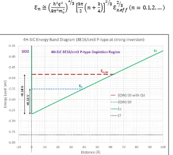
Figure 2.3: Energy band diagram of 4H-SiC MOS capacitor at strong-inversion
2.2.2 The Ideal MOS Capacitor Exact Charge Theory.
An ideal MOS capacitor is assumed for model development where all charges in the gate metal are exactly balanced by the induced charges within the semiconductor material and there are no other charges present in the system. Later, practical aspects including impacts of a metal-semiconductor work function difference and presence of undesirable impurities / charged states will be added to the ideal model.
The relationship between the charges present inside the semiconductor to the surface potential at the semiconductor surface will now be derived. Starting with Poisson’s Equation 2.10 (where ρ is charge density, ϵsc is the permittivity of the semiconductor, and q the elemental
depletion region where full-ionization is assumed, the p-type doping density, Na, is substituted
for the bulk equilibrium hole concentration p0. This is assumed valid given the surface potential
at strong-inversion creates an electric field in the semiconductor with magnitude greater than the ionization energy of the dopants (depletion approximation). Likewise, Na is substituted for p0 in
Equation 2.13.
𝑑2𝜙 𝑑𝑥2 = −
𝜌(𝜙)
𝜖𝑠 = −
𝑞
𝜖𝑠𝑐(𝑝 − 𝑛 − 𝑁𝑎
−+ 𝑁
𝑑−) Equ. 2.10
𝑝 = 𝑝0𝑒−𝑞𝜙 𝑘𝑇⁄ Equ. 2.11
𝑛 = 𝑛0𝑒𝑞𝜙 𝑘𝑇⁄ Equ. 2.12
𝑛0𝑝0 = 𝑛𝑖2 Equ. 2.13
Applying the chain rule to Poisson’s Equation in 2.15 and then substituting in an
alternative form of Poisson’s Equation 2.14, a derivative form of the electric field with respect to the potential is determined (Equation 2.15).
𝑑2𝜙 𝑑𝑥2 =
𝑑 𝑑𝑥(
dϕ 𝑑𝑥) = −
d
𝑑𝑥ℇ Equ. 2.14
𝑑2𝜙 𝑑𝑥2 = − (
dℇ 𝑑𝜙) (
dϕ
𝑑𝑥) = ℇ ( dℇ
𝑑𝜙) Equ. 2.15
In combining relationships 2.10, 2.11, 2.12, 2.13, and 2.15, an integral form of Poisson’s equation is set-up (Equation 2.16). Then, integrating (Equation 2.17), evaluating, and applying Gauss’s Law (Equation 2.18), the final relationship of semiconductor space charges as a function
of the surface potential is produced (Equation 2.19).
∫ ℇ𝑑ℇ0ℇ0 = − 𝑞
𝜖𝑠𝑐∫ (𝑁𝑎𝑒
−𝑞𝜙 𝑘𝑇⁄ −𝑛𝑖2 𝑁𝑎𝑒
𝑞𝜙 𝑘𝑇⁄ − 𝑁
𝑎+ 𝑛0) 𝜙𝑠
0 𝑑𝜙 Equ. 2.16
ℇ0 = ±√2𝑘𝑇𝑁𝑎 𝜖𝑠𝑐 [(𝑒
−𝑞𝜙 𝑘𝑇⁄ +𝑞𝜙 𝑘𝑇) +
𝑛𝑖2 𝑁𝑎2(𝑒
𝑞𝜙 𝑘𝑇⁄ −𝑞𝜙 𝑘𝑇)] 1 2 ⁄ | 0 𝜙𝑠 Equ. 2.17
𝑄𝑠𝑐 = ±√2𝜖𝑠𝑐𝑘𝑇𝑁𝑎[(𝑒−𝑞𝜙𝑠⁄𝑘𝑇+ 𝑞𝜙𝑠
𝑘𝑇 − 1) + 𝑛𝑖2 𝑁𝑎2(𝑒
𝑞𝜙𝑠⁄𝑘𝑇−𝑞𝜙𝑠 𝑘𝑇 − 1)]
1 2 ⁄
Equ. 2.19
Figure 2.4: Semiconductor charges as a function of surface potential.
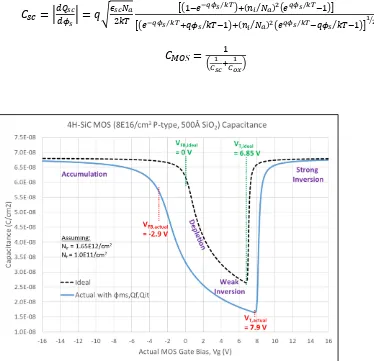
In Figure 2.4, the relationship between surface charges and surface potential (Equation 2.19) is plotted for the 4H-SiC MOS structure in the mobility study with p-type doping of 8x10¹⁶/cm3; also shown are the biasing modes with dominant ϕs dependencies. Note that for
![Figure 2.12: 6H-SiC electron surface mobility with surface coulombic scattering [6][23]](https://thumb-us.123doks.com/thumbv2/123dok_us/1173700.1147537/78.612.73.418.129.376/figure-sic-electron-surface-mobility-surface-coulombic-scattering.webp)
![Figure 2.13: 4H-SiC surface electron mobility scattering components & cumulative impact [6]](https://thumb-us.123doks.com/thumbv2/123dok_us/1173700.1147537/79.612.73.415.209.456/figure-surface-electron-mobility-scattering-components-cumulative-impact.webp)