r----t----,
I BUG S I L - - - t - - -JThe Brown University Graphics System1
The BrOWii Onive~sity Gca~hlc~ ~Loj~cL
Division of Appli~d Mathematics
Box F
Brown University
Provide~ce, Rhode Island 02912
June 1975 Printed: November 28, 1975
_
...l~his Research is being supported by the National science Foundation Grant GJ-41539, the Office of Naval Research, Contract N00014-75-C-0427, and the Brown University Division of Applied Mathematics; Principal I nvestigator Andries van Dam.
-1 Overview
The SH1ALE is a processing element of the BUGS system capable of performing a varied and complex repetoire of graphics opera tions for the user. Its high speed gives BUGS the performance typical of graphics systems employing special purpose hacdware but none of the inherent inflexibility. Although anyone could program the SINALE to meet the needs of his application, i t is presumed most users will use a standard set of SIMALE graphics operations embedded within a higher level language . The discussion that follows, therefore, is intended for the more serious user.2 SINALE Components
The SI~lLE's architecture departs radically from the more traditional ones of the Meta 4A and Meta 4B in several respects. These departures were dictated by the special nature of the graphics operations it performs. Speed, flexibility, simplicity, reliability, and cost were all important design considerations affecting its architecture.
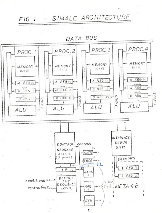
The most noticable features of the SIMALE are its abundances of processors, stores, and data buses (see figure 1). The SIMlILE has four parallel processors, quadrupling i t s effective speed, and unfortunately makinq it difficult to ulld~~stan~ a~J ~~0qram.
2.1 SINALE Stores
Tile SItHLE has four general types of stores; two in the control and two in the processing units.
~Q~!RQ1 ~1Qg~: This is a fully reajable/~riteable store in the control unit and is used primarily to hold instructions. I t consists of 256, 16-bit words orqanized into two, 128-word pages which are loaded hy the Meta 4B during execution of the ETC
instructiofl. Control storage locations may be read or written under SIMALE program control, although the addressing mechanism makes doing so difficult.
•
FIG
I
S
/M
ALE
ARC HITECTURE
OA TA BUS
-.
-
,_
PROC. I
r-
J
PROC. 2
-
__PRO'"
v .3
-~
PROC.
4
-<:..
.... MEMORY <l_ ...
NfMORY-,I.. IG x Ii?
" ~
-L <>-- .MEMORY
I*-CONTROL address
fNTfR FACEi
DEBUG
UNI;
conddfons»
STORAGE
;;(3(,<16 (2 f"'le<)
DECODE.
AND
. ' S £QC:::N(E
instruction set whil~ avoiding a more expensive
and inefficient · "horizontal" architecture.
£RQ~~2~2R ~~tlQRI: Each processo~ po~sesses sixteen,
18-bit words of memory used as a "scratch-pad" to hold less frequently used operands. The memories
are addres~ed by the MAR control register. All operand st.ores in the SHIALE are 18 bits to
provide the precision necessary tc avoid overflow problems arisinq during certain graphics
operations. The eiqhteen bits of these stores are
label ed (XO), (X1), (0), (1), ••• , (15) to emphasize
their positional relationship with the sixteen
bits of control storage and the Meta 4B.
£RQ~g~~QR BgGI~lliB2: In addition to the sixteen memory
locations, each processor has three 18-bit
reqist ers; the A, Q, and B re~isters. Two of these reqister s are shiftable and all are used for intermediate results and frequently used data
durinq computations. 2.2 SIMILE procesciors
The SIMALE has five loqical processinq units: one processes iu5tL~~~ivn3, auG fvu~ p~ocaS3 cpc~and data.
lli~lRY~lIQli RRQ~~~~QB: All instructions in the SIMALE are processed by the control unit. The execut ion of an instruction can cause activity on all of the
four operand processors simultaneously. This
parallel execution of instructions makes the SIMILE an efficient machine for graphical operations.
Q~gRaliQ £RQ~g~~QB~: Each of the processing units has an
18-bit ALIT (Arithmetic/Loqic Unit) which selects operands , from among the va rious stores and performs an arithmetical or logical operation upon them. The AUFR control register determines the
operations performed by the ALU'S. The results are made available on the F-buses where they can be copi ed into a store or t ested by subsequent
instructions.2 .3 The Data Bus
The SINALE transfers data amonq its various processing units
bits(S-1S) of the current i nstruction are copied onto the corresponding bits of the Z-bus and the rest are forced to zero. An additional data path serves to pass command, status. and debugqing information between the Meta 4B and the S!M~LE's control unit.3 THE SIMALE INSTRUCTION SET
The SIMALE has sixteen instructions, all of which are
16-bits long. Almost all instructions are divided into three fields; an operation code in bits(O-3). a modifier or data field in bits (1.-7), and an address field in bi ts (8-15). While most SINALE instructions are simple register loads. they can be difficult to understand because several things modify their behavior.
First. the loading of residual control registers determines the operation of subsequent instructions. E'or example. the setting of the AUPR register might instruct the ALU's to perform addition on the Band Q registers. If an instruction then loaded the A registers, they would contain the result of this addition. But for other settings of control registers, this same instruction could zero the A register, perform a logical OR 'ing
of two registers, or complete a data transfer with the Meta 4B. In addition, many of the control registers are cn top of stacks and can assume di fferel,t values on different leveis of program execution!
Besides being affected by residual control registers, the execution itself of many instructions is conditional. Condition codes referenced by these instructions test one of sixteen conditions throuqhout the SIMALE and modify execution behavior according to the result. See Section 3.4 for a further
explanation of the condition codes.
In the instruction descriptions that follow, upper case symbols are predefined by the SIMALE assembl er to the hexadecimal
values annotated (#hex value) and optional symbols are enclosed in braces. All symbols are delimited by either blanks or commas. To produce obiect code. the assembler simply OB's together the
values of the symbols appearing on a line of code. Por more detail, see the SHIALE A ssambler Manual. 3. 1 Processor Instructions
Instructions with operation codes 8 through 15 affect the operand stores of the four processors. All interpret bits (4-7) as a condition code and bits (8-15) as a branch address unless the condition code specified pre-empts taking this branch. The EBCR control register enables the processors. and no action is ever
Erite Memorv from F-bus on condition WM <condition code>[ ,<label>]
r---T----~---,
I 8 I CC I ADDRESS 1
L - - ___ ~ ____ _ L _ _ _ _ _ _ _ _ ~
o " 8 15
&oad
Q
register from F-bus on condition LQ <condition code>[ ,<label>]r---T---r---,
I B I CC I A DD FE SS I
L _____ ~ ____ _ L _ _ _ _ _ _ _ _ _ ~
o 4 8 15
Load
A
register from F-bus on conditionLA <condition code>[ ,<label>]
r---T---T---,
l e i CC I ADDRESS I
L ____ - L ___ - - l -_________ J
o ~ 8 15
Load
B
register from F-bus on condition LB <condition code>[,<label>]r---.----~---,
I F l e e I ADDRESS I L __ - - - k ____ - L - _______ - - J
o 4 B 15
For these instructions, each enabled prpcessor takes the
local value of the condition code specified and if true, copies the current lILD output from the F-bus into the specified 18-bit
store. In the case of a Write Memory instruction, the exact
memory location writtffn is specified by the Memory Address
Register (MAR).
Unless modified by the condition code, execution resumes at the address specified by <label>.
1eft ~llift Q register, entering condition value LSHQ <condition code>[,~label>]
r---T---T---,
I L-____ 9 ~ I cc _____ ~ I ADDRESS __________ ~ I
Bight 2llift
Q
register, entering condition value RSHQ <condition code>[ ,<label>]r-.----r---r---,
I A I
cc
I ADDRESS I L _____ i ____ - i __________ ~o 4 8 15
18ft 2llift ~ register, entering condition value LSHB <condition code>[ ,<label>]
r---T---r---, I D I
cc
I ADDRESS I L _____ i _____ ~ __________ Jo 8 15
Bight 2llift
B
register, entering condition value aSHB <condition code>[,<label>]r---T---r---, I E I
cc
I ADD RESS I L _____ ~ ____ _ L _ _ _ _ _ _ _ _ _ _ Jo 4 B 15
;Ocr these ir.St!:'!lCti.O~S, '2'ach '?nabled prot:~ss(lr shif ts the
specified register ona position in the specified direct ion,
entering the local value of the condition code into the emptied end bit position.
Unless modified by the condition code, execution resumes at
the address Specified by <label>. 3.2 Control Register
Instructions
The following instructions, with operation codes 2 through
6, load and modify the residual control registers.
boad nemory hddress Begister with immediate
LMAR <data>r,<label>j
T---T----~---_,
I 4 I DATIII ADDRESS I
L _____ i _____ L __________ J
o 4 6 15
This instruction takes the data specified in bits (4-7) and
loads i t into the 4-bit. Memory Address Register (11~.R).
Execution resumes at the address specified by <label>.
, Tho MAR is a control register whose contents selects one of
the sixteen locations in the processor memories. It sits atop a
by a CALL instruction and from which the MAR may be restored by a
RETURN instruction.
The M1\R can be incremented by a MOOR instruction (see
section 3.3).
Load ~ognT Beqister with immediate
LCTR <dat3.>[ ,<label>]
r---T----~---,
I 5 I DATAl ADDRESS I
L _____ ~ ____ - L __________ J
o .. 8 15
This instruction takes the data
loads i t into the 4-bit ~ounI Eegister
specified in bits (4-7) and
(CT R) •
Execution resumes at the addrass specified by <label>.
The CTH is a control r egister used to control program
loopinq. It sits atop a 16-level stack in which the current value
of the CTR may be saved by a CALL instruction or from which the
CTR may be restor~d by a RETURN instruction.
The CTR can be decremented
liot ~oun~ (NCT) condition codas
and tested by the ~OUl\1 (CT) and
(see Section 3.4) •
This bits(4-15)
Load ALl! Eunction Eeqister with immediate
LAUFR <function>[, INV][, HND][ , + 1 ]
r----T--r--T-~-T-r---~
I 2 IS11S21II RICIFUllC I
L-___ ~ __ ~ __ L-~_i _____ J o • 6 8 9 10 15
instruction takes the immediate data specified in
and loads i t into the 12-bit ILU function ragister.
Execution resumes at the next seguential instruction.
The ILU function register is a control ragister selecting
the operand stores and the operation performed by the ALU's of
the processors. There. are several fields within the register. The
5-bit field in bits(11-15) selects one of thirty-two arithmetic
or boolean operations performed upon the two source stores
sel.ected by the fields in bi':s (4-7). A description of all
thirty-two functions can ba found in the SIMALE hardware
Princiles of Operation manual; those currently defined for the
<function>:
F=<s1> (#0:>00): This copies s1 onto the F-bus.
F=<s1> OR <s2> (#0001): This logically OR's the two sources .
F=<s1> OR_NOT <s2> (10002): This OR's s1 with the
compl ement of s2.
F= ONES (#0003): This sets the F- bus to a l l ones.
F=<s1> AND <s2> (#0004):
sour.ces.
This AND's the two
F=<s1> XNOR <s2> (#0006): This is the complement
of the exclusive OR of the two sources.
F= <s 1 > A ND _ N OT < s 2 > ( # 0 0 08): Th i sAN D's s 1 with
the co~plement of 52.
F=<s 1> XOR <s2> (#0009): This XOR' 5 s1 with 52.
F= NOT <52> (~OOI)A): This comolements s2.
F=<s1> NAND <s2> (#OOOB): This NAND's s1 and s2.
F= ZEROS (#OOOC): This sets the F-bus to a l l zer as.
F=<s 1> NOR <s2> (#OOOE): This NORS s1 with s2.
F=<s1> +0 (#00 10): This adds zero plus the carry in to s1.
F= NEG_ONE (~0013): This sets the F-bus to all
ones plus the carry in.
F=<s1> MINUS <s2> (#0016): This sets t he F-bus to
s1 minus s2 minus one plus the carry in.
F=<s1> PLUS <s2> (#0019): This sets the F-bus to 51 plus s2 plus the carry in.
F=<s1> THIES_2 (#001C): This sets the F-bus to s1
l ef t s hifted one place.
F=<s1> -1 (I001F): This sets the F-bus to 51 minus
,
\<31> : The first operand source for the above functions is selected by bits (4,5). the possible sources are:
F= t1E /I (#0000) : The memory
F=A (#0400) : The A register
P=Q (#0800) : The Q register
F=B (#OCOO) : The B register
<s2»: The second operand source for the above functions is selected by bits(Q,7). The possible sources are:
!'I
EM
(~OOOO) : The memoryA (110100): The A register
Q (#0200) : The Q reg iste r
B (#0300) : The B register
INV (#0080): Bit (8) is the invert bit (I) and inverts the carry in and function bits(12-15) See!l by processors 2 and 3. This has the effect of ~aking
the ALU's of processors 2 and 3 perform thi complpment of the function performed on processors
o
and 1. Thu5 it is possible, for example, to GO addition on processors 0 and 1 and at the same time do subtraction on processors 2 and 3.RND (#0')40) : 13 it (9) is the round bit (R) and i f set, the carry in to any processor that has right shifted ct one bit out of its B reg~s.er ' t- is inverted. This prevents roundoff errors during certain opera
..
. ~ons. 'This
bits(4-15) (EBCR) .
boad Jnable, ]us £ontrol ~egister
with immediate
LEBCR <enable or request><bus src><bus dst>
r--~---T~---~----' I 3 I E~/P.C IEI SRC lOST I
L ___ - L ____ _ L_L-___ ~ __ _ J
o ~ 9 10 13 15
instruction
and loails it
takes the i mmediate data specified in
into the Enable and Bus control Register
Execut ion resumes at the next seguential a,ddress.
The EBCR is a control reqister which deals with eeabl ing
processors and with data transfers on the Z-bus. The LEBCR
instruction does not actually perform a data transfer but rath€r determines what transfer will be performed bi the XFER condition
code.
,
\<enable>: IIhen a LEBCR instruction is executed with bit (9) (E) set, bits (4-7) are loaded into a 4-bi t
enable reqis~er each bit of which enables one of the processors. Usually al l processors are l eft enabled, but when not, disabl ed processors are unaffected by instructions and cannot be tested by
condition codes. The MOOR instruction can rotat~ r igh t the ena ble bi ts one place. The en able
register bits are:
pO
(;/0840) : enables Processor 0P1 (110440) : enables Processor 1
P2 (#0240) : enables Processor 2
P3 (#0140) : enables Processor 3
ALL (#0 FO 0) : enables Processors 0-3.
<request> : When a LEBCR instruction is execut ed and
bit (9) (E) is off, bits (4-8) are loaded i nto the
5-bit Reguest Code Reqister. Thi s register is used
by the SIMALE to r equest an operation of the !eta 4B. When an IFER condi tion code causes the SIMALE
to pause fo:: I/O with the Meta 4, the Q-interpreter examines the request code register and the CTR. It t hen perform.s the requested
operation, sometimes usi ng, the CTR as a modifier.
, \
codes are currently implemented in the Meta 4B
firmware, and requestinq illegal codes causes a
SIMALE interrupt • The possible request codes are:
QUIT (#0000): causes termination of the current
ETC instruction.
INTERRUPT (#0080): causes a SH!ALE interrupt, then
quits.
NEXT_BLOCK (#')010): causes the termination of the
current ETC block and resumes execution at
the next block.
NEXT_SUB_BLOCK ('0180): causes 'termination of the
current ETC sub-block and resumes execution
at the next sub-block.
GOTO PAGE (#0200): The SIMALE qi ves the Meta 4B a
SIMALE initialization half word via the Z-bus.
The Meta 4B then loads the requested control
store paqe if necessary and starts SIl1ALE
execution at the requested lecation. This is
an inter- vin:ual paqe iumfJ (see Section i6.3
of the Meta 4B manual).
GET_DATA (*0280): causes the Meta 4B to get the
CTR number of halfwords from the current
sub-block and qive them one at a time to the
SIMALE via the Z-bus. If the CTR is zero, an
interrupt is caused and execution is halted.
SET_VG_MODE (10300): causes the Meta 4B to issue a
mode order to the VG which i t reads from the SHI"!.E Z-bus.
SEND_ VG_Dl,TA (#0380): causes the tleta 4B to send
the VG t he CTR number of halfwords from the
SHIALE Z-bus. If the CTR is zero, an
interrupt is caused and execution is halted.
GET_REG (#041)0) , PUT_REG (10480), GET_LS (1I0500),
PUT.:.I.S (~0580), GET_MS (#060'), PUT_MS
(#0680) , GET_VG_REG (#0700) , PUT_ VG_REG
(1078J): All of these request codes cause the Meta 43 to read an address from the SI MALE's
Z-bus. It then transfeI:s the eTR number of
halfwords to or from the specified stores
(ie. user REGisters , Local S.tcce, Main Store,
interrupt is caused and execution is halted.
of atop
by a be <bus src>: Bits (10 -12)
source. They sit
they may be saved
which they may
instruction. The incremented by the
the BECR select the Z-bus a 16-level stack in which CALL instruction and from
restored by a RETURN source nits may be
instruction. possible bus
MODR sources ar e:
FROM_M4 (10000) : Meta 4 is source
FROM_CS (#0008): control Store is source
FROM_IR (#0010): The low instruction is source
order byte of the
FROM ALL (tc(,018): The F-buses of all processors
are OR-ed toqether and are the source
FROM
-
PO (110020) : The F-bus of Processor 0 issource
FF. OM
-
P1 (110028) : The F-bus of P,OC8ssor 1 is sourceFROM
-
P2 (#0030) : The F-bus of Processor 2 issource
PROM
-
P3 (110038) : The F-bus of Processor 3 is source<bus dst>: Bits (13-15) of t.he, EBCR select the Z-bus
destination. As with the bus source field, the bus
destination bits are at.op a 16- level stack ann may
be incremented by the rODR instruction. possible
destinations are:
TO_~14 (#0000): Meta 4B is t.he destination
TO_CS (#0001): control store is the destinat.ion.
Bits(8-15) of the instruction invoking the
data transfer (ie. specifyinq xfer) is t.he address of the location leaded from the
Z-bus.
TO_ALL (ff·)003): The Z-bus contents is copied ont.o
t~e F-buSAS of all processors, which are not.
I
I
i
I
TO_PO (#,)004): The Z-bus is copied onto processor
O's F-bus, if not bus source.
TO_P1 (#0')05): the Z-bus is copied onto processor
1's F-bus, if not bus source.
TO_P2 (#0006): the Z-bus is copied onto p~ocessor
2's F-bus, if not bus source.
TO_P3 (#0007): the Z-bus is copied onto processor
3's F-bus, if not bus source.
tlQQify Begisters
MOOR [:1AR][,ENABLE][,SRC][ ,DST][<,label>]
r---r---r---,
I 6 I ~lAS K I ADD RE SS I
L _____ ~ __ ~ __________ J
o 4 8 15
The Modify Registers instruction uses bits (4-7) as a mask to
determine which of four control registers to modify as follows:
The control
address.
MAR (#()800): If bit (til is set, the Memory Adcl.ress
Register is incremented.
ENi\DLE (~0400): If bit(S) is set, the Enable field of
the EBCR bits (4-7), i s rocated right or.e position.
EBCR bit (7) is entered into EBCR bit (4) when this
is don"!.
SRC (#0200): If bit (6) is set, the source field of the
EBCR is incremented if the source specified is one
of the processors. Processor 3 wraps around to
Processor
O
.
DST (#0101) : I f bit (7) is set, the Destination field of
the EBCR is incremented if the destination
specified is one of the processors. Processor 3
wraps around to processor
O
.
3.3 Flow of controlInstructions
SIMALE has three
in programs. All
These instructions
instructions which
of them interpret
are:
alter the flow of
The condi tion execution execution
Ilanch on condition true
BR <condition code>[<,label>]
r---T----~---, I 1 I cc I ADDRESS I
L ____ - i ____ - L ________ - - J
o ~ 8 15
Branch instruction tests the global value of the code specified (see Section 3.4). If i t is true, resumes at the address specified by <label>, otherwise resumes at the next seguential instruction.
CALL subroutine
CALL [MAR1[ ,CTR]r ,SRCl[ ,DST][<,hbel> ]
r---T----~---, I 7 I MASKI ADDRESS I
L _____ l _____ L _________ - J
o
•
8 15The call instruction saves the next sequential address in a
16-level stack internal to the control unit. This serves as link
informfttion used by the RETURN instruction.
Execution is resumed at the address specified by <label>.
The CALL instruction also affects those centrol registers that are on stacks. The values of these control registers are constantly being copied into the present level of their stacks.
When a CALL is executed, the stack frame pointer is incremented,
accessing the next level of the stacks, then bits(4-7) determine the s~bseguent settinq of these control registers as follows:
,
\
~lAR (#0800): If bit (4) is set, the Memory Address Register I s curren t val ue remains unchanged. If bit (4) is not set, the MAR is loaded from the new stack level and thus assumes the value it had previous to the last RETURN •
CTR (#0400): If bit (5) is set, the count P.egister
r emains unchanged. If not set, the cra assumes its
previous value.
sac (#0200) ~ If bit (6) i s set, the source field of the EBCR r emains unchanged. If not set , i t assumes its previous value.
DST (#0100): If bit (7) is set, the destination field of
the EBep remains unchanged. If llot set, i t assumes
RETURN from subroutine on condition true.
RETURN <condition code>[<,label>]
r---T----~---~
I 0 I CC I A DD HE 55 I
L - -___ ~ ____ ~ _________ ~
o ~ 8 15
The RETURN instruction tests th8 global value of the
condition code specified. If i t is true, the stack frame pointer
is decremented and the control registers are restored to their
values previous to the last CALL instruction. Execution is
resumed at the saved address. If the condition code is not true,
execution is resumed at the address specified by <label>. 3.4
Condition Codes
The SIMALE conditional instructions specify a condition code
in bits(4-7). All cod"s select one of sixteen conditions t9sted
in five pl~ces; in the control unit, and in each of the four
processors. The valu9 tested in the control unit is called the
global value, and the values tested in the processors are called
the J.ocal values. In many cases, the global value is simply the
logical OR 'ing of the four local values. Disabled processors make
no contribution to the global values so obtained.
Four of the condition codes can modify the operation of
proc0ssor-type instructions. This modification usually involves
invoking special cycle seguences or altering where execution is
resumed upon completion. The condition codes are:
FALSE (#0000) : This doesn't modi::y instruction
sequencing
local value: always false
global value: always false
TRUE (110100) : This doesn't modify instruction
sequencing
local value: always true
qlobal value: always true
TREJ (#0200) : This is a windowing re jection test for a
line whose end point window coordinates are in the
A an,j Q registers. If both of these registers are
neqative on anyone processor, then the line is
absolutely outsid8 the window. TREJ doesn't modify
local value: (t. (XO) AND Q (ZO» from all enabled processors OR'd together
global value: same as local value.
REJ (10300): This is a windo'.ling rejection test for a
line whose window coordinate end points are in the
A reqister and on the F-hus. If both are negative
on anyone processor , the line is absolutely
outside t he wi n dow. R EJ doesn I t modify i nstr uction
sequencinq.
local value: (A (XO) AND F (XO» from all enabl ed
processors OR' d together
global value: same as local value
DELAY (#0400): '!Chis
the execution
fixinq possible
inserts a one cycle delay of a processor i nstruction
proqram timinq problems.
local value: always true
qlabal value: 31~3Vs tr~e
before to aid
XFER ('0500): When referenced by a processor
instruction, ZFER triggers a several cycle
sequence causinq a data transfer al ong the Z-bus. The transfer is from the source to the destination as specified in the EBCH. If the t'leta 413 is
invblved, the SIMALE pauses unt i l the Meta 4 can
siqnal the transfer is compl ete. Only those
processors which are destinations call be affected
by an instruction specify ing XrES, and only those
which are sources pay attention to the setting of
the AUPR ~urinq the transfer.
Execution is always resumed at the next sequential
i nstruction.
local value: always true
qlobal value: always true
CT (#0600): The CounT condition code always causes the
eTR to be decremented. If i t i s speci fied by a
processor instruct ion, and the CTR was one before
beinq decremented, exec ution is forced to resume
at thO! next seq·uential instructicn; .otherwise i t
resumes at the address specified. This gives
,
\
local value: always true
global value: CTR not = 1 (i.e. goes fa~se when
the count is exhausted)
NCT (#0700): The Not Count condition code always causes
the CTR to be decremented. If it is specified by a
processor instruction, and the CTa was one before
bein 9 deer ement ed, execut ion is forced to resume
at the r.ext seguential instruction; otherwise it
resumes at the address specified. This gives
processor type instructions a 8CT ability.
local value: always false
global value: CTa = 1 (i. e.,
count is exhausted)
COUT (#0800):
sequencing.
This doesn't
gOES true when the
modify instr uction
local valrio: £arry
QQ!
from ALU bit(XO)q10bal value: carry nut
processors OR'd together.
NP(XO) (#0900):
seguencing.
This doesn't
from all enabled
modify instructions
local value: the complement of the sign bit of the
F-bus
global value: NF (XO.) 's of all enabled processors
OR'd toget her
LSIG (#n00):' This doesn't modify instruction
seguencing. LSIG i s a test for left significance
of a processor's S reqister (i.e. , e!.ther i1:s left
most two bits are different or it is all ones or
zeros)
local value: (B(XO) xoa S(Xl» OR (8 NOT MIXED)
global value: LSIG's of all enabled processors
OR'd together.
BM (IOB00): This doesn't modify instruction sequencing.
D mi xed is a t e.st f::>r a processor's 8 H'!gister not
baing all ones or all zeros.
global value: BM of all enabled processors OR' d
together.
Q(XO) (~OCOO), Q(15) (#0000),
B (15) (#OPOO): These ·don't
sequencing they ar e used to the Band Q register.
local value: the bit specified
B (XO) (#OECO),
modify i nstruction
test the end bits of
global value: the bit specified of all enabled