Analog and Mixed Signal Test Method based on OBIST
Technique
Mradul Kumar Ojha
M. Tech. (VLSI Design) Student, Electronics Department, I.T.M. College, Gwalior (M.P.), India
Shyam Akashe
Associate Professor, Electronics Department, I.T.M. College, Gwalior (M.P.), India
ABSTRACT
This paper describes a test method for analog and mixed signal device at very low cost and it‟s based on OBIST (oscillation test) method. This method is built-in self test method appropriate for functional and structural testing of analog and mixed signal circuit. In test mode, the test circuit is converted into an oscillator. Then faults inside the test circuit that cause an affordable deviation of the oscillation frequency from its value are detected. Through this test method, no test vector is required to apply. Therefore in this test technique, the test vector generation drawbacks are eliminated and also the test time is reduced because limited number of oscillation frequencies is evaluated for each test circuit. This characteristic implies that Oscillation-test methodology is very attractive for further wafer-probe testing as final production testing. During this paper, the simulation results of this test method has been provided and verified throughout some examples like CMOS inverter and FET (field effect transistor).
Keywords
Built In Self Test (BIST), Oscillation Based Built In Self Test (OBIST), System On Chip (SOC), Design For Testability (DFT), Integrated Circuit (IC), Circuit Under Test (CUT).
1. INTRODUCTION
The development of mixed signal integrated circuit technology in System on Chips (SOCs) and market requirements have motivated the system designers and the test engineers to shift their research direction in this particular area of very large-scale integrated circuits and develop system specifically for effective test methods. Analog testing is considered as the most significant drawback in analog and mixed signal device and is also a challenging task. The main sources of test difficulties in digital and analog circuits are totally different. The size and complexity in digital circuits remain a measure of test difficulty whereas in analog and mixed signal circuits, the behavior of circuit signals area unit is far more necessary than the circuit sizes. A significant downside within the analog and mixed-signal-circuit testing is in defining the line of demarcation between a fault-free and faulty circuit, which results in uncertainty in quantification of the product yield. In the part of digital circuits, some imperfectness area unit is unimportant, but within the mixed signal analog circuits, small imperfections such as small capacitance between the traces can present a major circuit‟s component which can change the circuit‟s performance. Testing ensures the quality of product when it is implemented during key phases of product development. Testing for analog circuits is often accomplished using, functional testing, DC testing, power supply current monitoring and Digital Signal Processing (DSP) techniques. Several Design for Testability (DFT) techniques are developing to extend the testability and controllability while to reduce the number of test problems, test buses and scan chain methods are also used [1]. But the
above techniques strongly depend on the selection of suitable test vectors. When the complexity of the circuit under test increases, the problem of generating the optimal test vectors assuring the high faults coverage becomes critical. Therefore the test outcome will be incorrect and production yield will be decreased. Furthermore, the process of choosing a suitable form of excitation signals and results analysis is time intense. Built-in self-test technique based on the existing test methods require the use of specialized input stimuli generation and output analysis hardware which introduces a major space overhead. BIST is a design process that provides the capability of solving many of the problems otherwise they can be encountered in testing analog, mixed-signal or digital systems. In BIST, test generation, test application and response verification are all calculated through built-in hardware that permits the different part of the chip to be tested in parallel thereby reducing the test time and also eliminating the requirement for external test equipment.
Typically, analog circuits are tested by verifying against specifications. Test inputs may be generated simply for this straight forward methodology. The lack of standard fault model for elements of analog or mixed-signal circuits, wideness of analog specifications and incomplete test set could, however, decrease the test quality for the analog portion. Another major problem in testing analog components is in defining the line of demarcation between a fault-free and faulty circuit, resulting in uncertainty of quantification of the product yield [2]. Testing for all specifications is time consuming and valuable. Since the analog and mixed signal circuits are complicated, some effort is to be taken to lower the value of test, particularly for the analog parts of mixed signal circuits. Nearly each mixed signal integrated system contains circuits like operational amplifiers, filters, oscillators, Phase lock loops, etc. During this paper, an approach to develop a test method for analog and mixed signal circuit based on oscillation based BIST is investigated. Throughout the test mode, all these circuits could be transformed to an oscillator by connecting some additional circuitry (a feedback network). Within the method, the outlined faulty model and test process are considered to test the circuit in analog and mixed signal device and simulation results are provided for selective benchmark circuits.
2. PREVIOUS WORK
simply ending in abnormal specifications. Previously, several fault based test strategies have been planned within the literature for testing analog and mixed signal circuits. Various techniques are developing for DFT; all techniques are different in their approach and all of them have a similar aim of raising the testability of IC design. Some testing approaches are Ad-hoc test, Scan-based test (Path-scan, Boundary-scan) and Self-test (Built-in self-test, Built-in logic observation).In this paper we have used, OBIST method for detecting the hard faults called catastrophic faults in mixed signal circuits. The OBIST deserves a special mention as a result of its conceptual straight forwardness and does not require extensive modification of CUT for testing.
3. TEST METHODS
3.1. Design for Testability (DFT)
[image:2.595.69.273.307.395.2]Design for Testability (DFT) methodologies can cast into two types (a) those that rely on reconfiguration of the Circuit under Test (CUT) for testability improvement and (b) those that rely on test point insertion for controllability and testability of the inner nodes of the CUT [4].
Fig 1: Design for Testability
DFT methodology refers to hardware design style or value added hardware that reduces test generation, quality, complexity and test application cost. The basic concept design for testability is given in figure (1). The test generation complexity will increase exponentially with the size of the chip. To increase the testability and controllability of internal node, test buses, scan chain method are used while other useful methods are also developed [5- 6].
3.2. General Built in Self-Test Structure
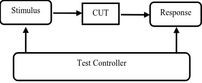
It is a design process that provides the capability of solving the problem otherwise encounterd in testing analog and mixed signal devices. In BIST, test generation application and test response verification are accomplished through in built hardware. It permits the various parts of the chip to be tested in parallel, thereby reducing the specified test time. It also abrogates the requirment for external test equipments. The cost of testing is turning into one major part of producing expense of the new product. BIST tends to reduce the manufacturing and the maintenance costs through improved identification [7]. A BIST environment, as in displays figure (2), uses a test pattern generator (TPS - stimulus source) that sends its output to a CUT and output stream is fed into a test data analyzer.
Fig 2: Typical BIST Structure
A fault is detected if the test sequence is totally different from the response of the fault free circuit. The test data at information instrument comprises of a Response Compaction Unit (RCU), storage for the fault-free responses of the CUT and comparator. In integratedcircuits, BIST is used to create quicker, more cost-effective producing tests. As a result of BIST this mechanism allows a machine to check itself. A BIST mechanism is provided in advanced field bus systems to verify its functionality [8- 9]. It reduces the test-cycle period.
4. OSCILLATION BASED BIST OF
ANALOG/MIXED SIGNAL CIRCUITS
(OBIST)
The test methods for analog and mixed signal circuits are based on rearranging the CUT to an oscillator. During this method, the complicated analog circuit are partitioned into functional building blocks such as: operational amplifier (Op-amp), Schmitt trigger, filter, voltage reference, oscillator, phase lock loop (PLL), etc or a combination of these blocks. During the test mode, each building block of circuit is converted into an oscillator by adding the proper circuitry in order to achieve sustained oscillation. The oscillation is then evaluated [10].
[image:2.595.318.539.376.573.2]The fault is revealed from a deviation of its oscillation parameters with reference to the parameters below the fault free conditions. The oscillation parameters are freelance of the CUT type and analog testing [11-12]. The block diagram of OBIST strategy is illustrated in figure (3).
Fig 3: Block Diagram of OBIST
5. TESTING PROCEDURE FOR OBIST
The application of testing procedure is proposed in this paper. Catastrophic faults (stack open and stack short) are injected into the CUT. These faults after being injected into the nominal circuit descriptions by using the simulator, evaluates the transient response while frequency and output voltage are measured. The fault free circuit is converted into an oscillator and simulated and its test parameter is thus derived. The different steps of the procedure are briefly given below [13- 14].
The different steps of the procedure are -
The fault free circuit was converted into oscillator and simulated, and test parameter is derived.
A fault list was derived from the CUT.
The faulty net list was generated (through faults injected into the CUT).
Feedback circuit Faulty
CUT
Feedback circuit
Fault Free CUT
Obtained Oscillation Parameters
Normal Oscillation Parameters
Comparison and Decision
Stimulus CUT Response
Test Controller Logic
Block A
Logic Block B Internal Bus
PI PO
[image:2.595.66.265.661.743.2] A simulation was done for the faulty CUT.
The fault detection was completed on comparing the faulty output measurements with fault-free test parameters.
The circuit fault coverage was calculated.
6. CASE STUDIES AND RESULTS
To be able to calculate the proposed test methods we first define the fault modeling. Then some analog and mixed signal building blocks are used as test to examine the efficiency of test method, but the method is by no means confined / restricted to these examples in its application.
6.1. Experimental Result of Inverter and
Oscillation-Frequency Calculation
Analog ICs consist of an amplifier, a filter, PLLs, comparators, etc. The test parameter specified by designers can be gain, phase shift, signal to noise margin, power gain, gain margin, phase margin and so on. Efficient ways test operational amplifier and filters are desired because of their importance in analog systems. If we take a look at the, test methodology of any circuit which is oscillation based, we can observe that, first of all the CUT is partitioned into the functional building blocks.
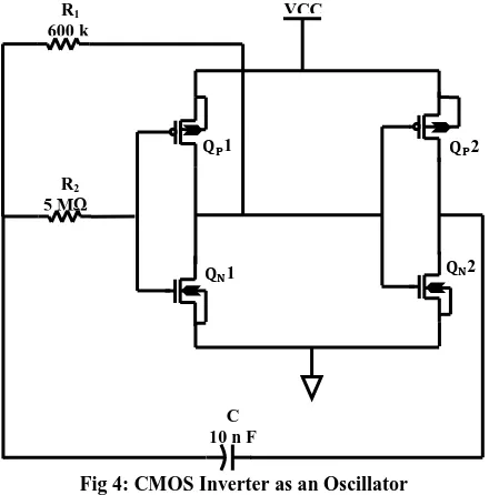
[image:3.595.318.549.386.522.2]Then each building block of CUT is converted into oscillator by the addition of extra circuitry as a feedback. If the circuit is faulty then converted circuit is either doesn‟t oscillate or the responses parameters of oscillation can completely differ from the fault free circuit. The proposed OBIST methodology for calculating the oscillation frequency is explained by considering the example of CMOS inverter circuit to oscillate where the classical CMOS astable-oscillator concepts are employed. A CMOS inverter is converted into astable-oscillator using one more inverter and one RC feedback. As shown in figure (4), the R1 resistance connects the output of the CMOS inverter to its input and it acts as dc negative feedback. The output of the CUT inverter is connected to the input of another inverter U1. This provides the positive ac feedback.
Fig 4: CMOS Inverter as an Oscillator
The oscillation frequency of CMOS inverter can be determined as follows:
During time interval t1, when the output is low, the voltage
across the capacitor rises from Vcc /2 to Vth
Substituting, vc = Vth= VCC /2 at t = t1
t1 =R1C1 ln3 (1)
Also the time interval t2, when the output is high, vc falls from
3VCC/2 to Vth.
Substituting, vc = Vth= VCC/2 at t= t2
t2 = R1C1 ln3 (2)
The total period of output can be achieved by adding (t1 and
t2) as
T = t1 + t2
From eqn. (1) and (2) T= 2 R1C1 ln3
T = 2.2 R1C1 (3)
The oscillation frequency is expressed as fosc = 1T
fosc = 1/ 2.2 R1C1 (4)
By choosing R1= 600 kΩ, C1= 10 nF and R2= 5 MΩ, the
oscillation frequency of CMOS inverter can be calculated as fosc = 90.9 Hz.
The fault model for MOS transistors, where the value for the parallel resistor Rp is 10 Ω and which emulates stuck-short
fault, and the series resistor Rs which has a value of 100 MΩ
[image:3.595.57.277.488.711.2]that emulates stuck-open fault, is shown in figure (5).
Fig 5: Four Fault Models for PMOS and NMOS Transistors of Inverter
Now, we consider the hard or catastrophic fault injected into the CUT in test mode. Injecting the four faults specified in CUT test mode cause stopping of the oscillation of the circuit. If any one of the transistor is short or open, the output will be low or high according to the types of fault. All simulation results obtained below agree with this hypothesis.
6.2 FET (Field-Effect Transistor)
Here, oscillation test method has been used to test the field-effect transistor. In this section, phase-shift oscillator is used for OBIST method. The phase-shift oscillator produces the positive feedback by using an inverting amplifier and adding another 180° with the three high-pass filter circuits as shown in figure (7). It produces 180° phase-shift for only one frequency. The field-effect transistor provides a negative gain amplifier with 180◦ phase shift, and each RC pair results in 60° phase shift.
The basic RC oscillator that is additionally referred to as a phase-shift oscillator produces a sine wave output signal victimization regenerative feedback obtained from the arrangement of resistor and capacitor. This regenerative feedback from the RC network is attributed to the
RP
10 Ω QP
RP
100 k Ω
QN
QN
RP
10 Ω 𝐐𝐏
RS
100 k Ω VCC
R1
600 k
Ω
R2
5 MΩ
𝐐𝐏1
𝐐𝐍1 𝐐𝐍2
𝐐𝐏2
flexibility of the capacitance to store an electrical charge. This resistor-capacitor feedback network is connected as displayed in figure (6) to produce a leading phase shift (phase advance network) or interchanged to produce a lagging phase shift (phase retard network). The result is still the
Fig 6: Phase Shift Oscillator in Test Mode
same as the sine wave oscillations only occur at the frequency at which the overall phase-shift is 360o.
Through one variable one or a lot of the resistors or capacitors within the phase-shift network, the frequency will vary and usually this can be done by keeping the resistors constant and employing a 3-ganged variable capacitance. If all the resistors R and also the capacitors C within the phase shift network are equal in value, then the oscillation frequency is produced by the RC oscillator given as oscillation frequency (fosc).
fosc = 1/ (2π RC 2N) (5)
Where, N is number of RC stages. (N = 3).
By choosing R1= 10 kΩ, C1= 3 nF and R2= 3 kΩ, R3= R4= R5= 10 kΩ, C2= C3= C4= 6.5 nF, the oscillation frequency
of FET oscillator can be calculated as fosc = 9.996 k Hz.
The bandwidth of a composite signal is the difference between the highest (fhishest) and the lowest frequencies (flowest) contained in that signal output.
Since the arrangement of resistor-capacitor in the phase shift oscillator circuit additionally acts as an attenuator producing an attenuation of -1/29th (Vo/Vi = β) per stage, the gain of the amplifier should be comfortable to beat the circuit losses. Therefore, in our 3- stage RC network above, the amplifier gain must be greater than 29. Table (1) indicates FET faults coverage analysis. The output waveform of phase shift oscillator are shown in figure (7)
0 0.5
1 1.5 2
0.005 0.01 0.015
T im e
V
o
u
t
Fig 7: The Output signal of Phase shift oscillator
The circuit stops the oscillation by injecting the faults into the transistor. Once the FET transistor is open, that is, it‟s disconnected from the circuit, the circuit doesn‟t oscillate. By injecting short faults within the circuit, the FET transistor operates within the cutoff region, as exhibited in figure (8). The given table represents the results obtained by the simulation for the transistor generator oscillator when the hard faults are injected. Once the FET is open, it‟s disconnected from the circuit doesn‟t oscillates. Fault is detected once the power bandwidth is out of tolerance band. Fault-free power bandwidth is 18.84.
Here, all possible faults represent the have not been thought-about. For the faults thought-about, 100 percent fault coverage was achieved.
Table (1) FET Oscillator Faults Coverage Analysis Faults Amplitude
(nV)
Bandwidth (µHz)
Power Bandwidth(Hz)
R1 14.9 26.86 42.3
R2 0.92 27.94 42.5
R3 7.75 26.85 42.7
R4 7.79 27.41 42.6
R5 7.72 26.82 42.6
C2 7.07 27.14 42.4
C3 7.26 26.65 42.8
Fault
[image:4.595.316.539.240.606.2]Free 14.80 10.70 18.84
Fig 8: FET Oscillator Faults Coverage Analysis
7. CONCLUSION
The OBIST techniques have been effectively utilized in analog and mixed signal circuits in embedded core based system on chip environments. There are many strategies to confirm the correct functioning of designed circuits, however this built in hardware approach has proven to be one of the most reliable strategies. This oscillation based technique is implemented where the hard and parametric fault models are defined for fault coverage analysis. The catastrophic faults are considered in this paper. By using power bandwidth,
0.00 0.20 0.40 0.60 0.80 1.00
Faults
FET Oscillator Faults & Faults Free Coverage Analysis
Amplitude(nV) Bandwidth(µH) Power Bandwidth(n Hz) Output
VCC
C1 3µF
R2
3 k R4
10 k
R3
10 k R5
10 k
R1
10 k
C4
6.5µF C3
6.5µF C2
[image:4.595.64.269.638.742.2]amplitude and oscillation frequency, we have observed improvement in fault coverage. Some sample benchmark circuits are simulated and studied. The results are verified in Simulation Software. The detection of faults in fault coverage shot up when the time domain output was converted to frequency domain and compared with the same ±5% threshold values. A very high coverage of 100 percent was achieved as well. The OBIST testing method has been applied for many circuits like analog to digital converter, dual tone multiple frequency detector, filters, voltage-controlled voltage source filter, switched capacitor circuits, etc. OBIST method does provide high-fault coverage with low-area overhead. It has been demonstrated that, the OBIST method is suitable for both functional and structural testing and has the potential of covering catastrophic and parametric faults. A structure presents a pass or fails result; it will be simply integrated with the test strategies dedicated to the digital, a part of the circuit under test.
8. ACKNOWLEDGMENT
The author would like to thanks Mr. Shyam Akashe of the Department of Electronics and Communication Engineering, Institute of technology and Management, Gwalior, India for his guidance and valuable suggestions in the design and simulation of the circuit for testing analog and mixed signal device and deep thanks to Cadence Pvt. Lmt. Bangalore for providing software simulator.
9. REFERENCES
[1] Jacob A. Abraham and Jeongjin Roh, “A Comprehensive Signature Analysis Scheme for Oscillation Test,” IEEE Transactions on Computer Aided Design, vol. 22, no. 10, pp. 1409-1423, Oct. 2003.
[2] M. H. Assaf, Sunil R. Das, W. Hermas and W. B. Jone, “Promising Complex ASIC Design Verification Methodology,” Proceeding of IEEE Conference on Instrumentation and Measurement Technology (IMTC), pp. 1-6, May 2007.
[3] S. R. Das, “Self-testing of Embedded cores-based Systems with Built-in Hardware,” Proceeding, Institute of Electrical Engineering- Circuit Devices Systems, vol. 152, no. 5, pp. 539-546, Oct. 2005.
[4] Andrew Richardson, “Design-for-test Strategies Analogue and Mixed Signal Integrated Circuits,” Proceeding of 38th Midwest Symposium on Circuits and systems, vol. 2, no. 4, pp. 1139-1144, Aug. 1995. [5] S. M. Saeed, “Design for Testability support for Lunch
and Capture Power Reduction in Lunch-off-Capture,” IEEE Transactions of Very Large Scale Integration (VLSI) Systems, vol. 22, no. 8, pp. 516-521, March 2014.
[6] I. Pomeranz and S. M. Reddy, “Transparent DFT: a Design for Testability and Test generation approach for Synchronous Sequential Circuits,” IEEE Transaction of Computer-Aided Design of Integrated Circuit and Systems, vol. 25, no. 6, pp. 1170-1175, June 2006.
[7] M. H. Assaf and Maryam Fathi, “Built in Hardware for Analog Circuitry Testing,” Electronics, Robotics and Automotives Mechanics Conference, no. 2, pp. 14-19, Sep-Oct 2008.
[8] S. Umezu and M. Hashizume, “A Built-in Supply Current Test Circuits for Pin opens in Assembled PCBs,” International Conference on Electronics Packaging (ICEP), pp. 227-230, April 2014.
[9] Sunil R. Das, “Self-testing of Embedded cores-based Systems with Built-in-Hardware,” Proceeding of IEEE Transaction on Circuit, Devices and Systems, vol. 152, no. 5, pp. 539-546, Oct. 2005.
[10]Daniel Arbet and Viera Stopjakova, Libor Majer and Gabriel Nagi, “New OBIST using On-chip compensation of process variations toward increasing Fault Delectability in Analog ICs,” IEEE Transactions on Nanotechnology, vol.12, no. 4, pp. 486-497, July 2013. [11]Sergio Callegari and G. Setti, “Complex Oscillation
based Test and its Application to Analog Filter,” IEEE transaction on circuits and systems, vol. 57, no. 5, pp. 956-969, May 2010.
[12]Miljana Milic, Vanco Litovski, “Oscillation based Analog Testing- a case study,” MIPRO, Proceedings of the 34th International Convention, no. 5, pp. 96-101, May 2011.
[13]Daniel Arbet and Gabriel Nagi, “Efficiency of Oscillation-based BIST in 90nm CMOS Active Analog Filter,” 16th
International Symposium on IEEE, Design and Diagnostics of Electronic Circuits & Systems (DDECS), no. 4, pp. 263-266, April 2013.
[14] Daniel Arbet and Juraj Brenkus, Viera Stopjakova, “Oscillation-based Built-in Self Test of Integrated Active Analog Filters,” International Conference, Applied Electronics (AE), no. 2, pp. 1-4, Sept. 2011.
[15]Jila Zakizadeh and Sunil R. Das, “Testing Analog and Mixed Signal Circuits with Built-in Hardware, A New approach,” Proceeding of IEEE Conference on Instrumentation and Measurement Technology IMTC 2005, no. 3, pp. 166-171, May 2005.
[16]Radoslaw M. Biernacki and Johan W. Bandler, “Multiple-fault Location of Analog Circuits,” IEEE Transaction on Circuits and Systems, vol. 28, no. 5, pp. 361-367, May 2003.
[17]Linda Milor and S. Alberto Vincentelli, “Computing Parametric Yield accurately and efficiently,” Proceeding of IEEE Conference on Computer-Aided Design, pp. 116-119, Nov. 2008.