Effect on Total Field Gain and VSWR Due To
Variation of Dielectric Constant of
Rectangular Microstrip Patch Antenna Using
IE3D Software
Manjari Bharati1, Hironmoy Das2, Debojyoti Sur3, Anjan Singh4, Arunima Mondal5
Assistant Professor, Dept. of ECE, Dr. Sudhir Chandra Sur Degree Engineering College, Kolkata, West Bengal, India1
UG Student, Dept. of E.C.E, Dr. Sudhir Chandra Sur Degree Engineering College Kolkata, West Bengal, India2
UG Student, Dept. of E.C.E, Dr. Sudhir Chandra Sur Degree Engineering College Kolkata, West Bengal, India3
UG Student, Dept. of E.C.E, Dr. Sudhir Chandra Sur Degree Engineering College Kolkata, West Bengal, India4
UG Student, Dept. of E.C.E, Dr. Sudhir Chandra Sur Degree Engineering College Kolkata, West Bengal, India5
ABSTRACT: This paper describes effect on total field gain and VSWR due to variation of dielectric constant of microstrip patch antenna. In this paper rectangular patch with probe to feed technique is used. In this paper we design and simulate a rectangular microstrip patch antenna operating at a frequency of 11 GHz. The rising importance of wireless communication and multimedia services increasing the efforts to the design and implementation of microstrip patch structures. A patch antenna is advantageous because of its low cost, small size, ease of fabrication, and can easily be integrated into many commercial transceiver systems. The performance of antenna is studied in terms of parameters like length, width, patch height of antenna. The paper describing how VSWR and total field gain can vary due to change of dielectric constant and gives a better understanding of design parameters of an antenna and their effect on return loss plot. Finally simulation is done using design software IE3D.
KEYWORDS: Microstrip patch antenna, probe feed, VSWR, gain, return loss, IE3D.
I.INTRODUCTION
Antenna is part of a transmitting or receiving system that is designed to radiate or receive electromagnetic waves. Microstrip antenna is only one such type of antenna. A microstrip device in its simplest form is a sandwich of two parallel conducting layers separated by a single thin dielectric substrate. The upper conductor is thin metallic patch (usually Copper) which is a small fraction of a wavelength. The lower conductor is a ground plane which should be infinite theoretically. The patch and ground plane are separated by a dielectric substrate which is usually nonmagnetic. Here the dielectric constant of the substrate ranges from 2.2 to 3.0. The patch can assume any shape such as rectangular, circular, triangular, elliptical, helical, circular ring etc. Microstrip antenna elements radiate efficiently as devices on microstrip printed circuit boards. Microstrip patch antenna consists of a radiating patch on one side of a dielectric substrate with a continuous metal layer bonded to the opposite side of the substrate which forms a ground plane. The patch is generally made of conducting material such as copper or gold and can take any possible shape. A patch antenna is a narrowband, wide-beam antenna fabricated by photo etching the antenna element pattern in metal trace on the dielectric substrate.
In telecommunication, there are several types of microstrip antennas(also known as printed antennas) the most common of which is the micro-strip patch antenna or patch antenna. A patch antenna is a narrowband, wide-beam antenna
possible. Some patch antennas do not use a dielectric substrate and instead are made of a metal patch mounted above a ground plane using dielectric spacers; the resulting structure is less rugged but has a wider bandwidth.
Because such antennas have a very low profile, are mechanically rugged and can be shaped to conform to the curving skin of a vehicle, they are often mounted on the exterior of aircraft and spacecraft, or are incorporated into mobile radio
communications devices.
Fig.1 The inner view of a patch antenna.
II. BASIC PATCH ANTENNA GEOMETRY
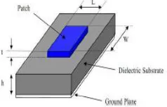
In its most basic form, a Microstrip patch antenna consists of a radiating patch on one side of a dielectric substrate which has a ground plane on the other side as shown in Figure 1. [2] The patch is generally made of conducting material such as copper or gold and can take any possible shape. The radiating patch and the feed lines are usually photo etched on the dielectric substrate.
Fig 2 Structure of a Microstrip Antenna.
III. FEEDING TECHNIQUES
The two techniques available to feed or transmit electromagnetic energy i.e. induce excitation to a microstrip antenna are contracting (feeding is done directly via a connecting element such as microstrip transmission line and co-axial probe) non contracting types (like aperture coupling, electromagnetic field coupling is done to transfer power between the microstrip line and the upper conductor.
A. MICROSTRIP LINE FEED TECHNIQUE
The simplest way to feed a microstrip patch is to connect a microstrip line directly to the edge of the patch. In this case both the patch and the lines are located on the same substrate. The matching between the characteristic impedance of the microstrip feed line and the patch can be done by selecting the right depth of the inset.
Fig.4 Patch antenna with microstrip line feed.
IV. FRINGING EFFECT
The radiation from microstrip antenna can be found from the patch spaced of a wavelength above a ground plane. When the length of the patch is about half a wavelength long, then the radiation generates from the fringing electronic fields between the patch and the ground plane. Further, it is assumed that there is no variations of electric field along the width and the thickness of the antenna. The fringing electronic field is an effect of the electrons congregated at the surface of the conductor, especially at the edge. So that most of the radiated power is distributed from the edge of the patch.
V. MODELLING TECHNIQUES
To understand and analysis the behaviour of microstrip antennas choosing model to simulate the performance is very helpful in antenna design stage. There are two types of modelling technique available.
1) Transmission line model
2) Cavity model
VI. FOUMULAS USED FOR ANTENNA DESIGNING
Here the formulas used for antenna designing are described below where W is the width of the proposed antenna, L is the length of the antenna ,ϵreff is the effectivepermittivity of the antenna, which is given by:
εreff= ( εr+1) /2 + ( εr-1)/2 *[1+(12(h/w)]-.05
Calculation of Length Extension ΔL, which is given by :
(ΔL/h) =0.412[(εreff+ 0.3)*((w/h)+0.264)]/ [(εreff -0.258)*((w/h)+0.8)]
For effective radiation , the Width W is : W= λg/2*[(εr+1)/2] -0.5
Now, to calculate the Length of patch becomes: L= {(λg/2)*(εreff)-0.5}-2* (ΔL)
The Effective Length of the patch Leffnow becomes : (λ0/ ʄ0)*( εreff)-0.5
Length and Width of ground is : Lg=6h+L & Wg=6h+W.
Where,
μ0=Permeability constant.
ε0=Permittivity of a free space.
εr=Relative permittivity.
h=Height of a patch antenna.
λg=guided wavelength.
VII. DESIGNING
First a simple rectangular microstrip patch antenna has been designed using IE3D software
Fig.5 Design of a Rectangular Microstrip Patch Antenna.
Design parameters are as follows:-
Patch length (L) = 12mm
Patch width (W) = 8 mm
Dielectric constant (ԑr) = vary from (2.2 to 3.0)
Substrate thickness (h) or patch height =1.5 mm
Center frequency=10 GHz
Probe feed distance (dp) =-3 mm (from centre)
Probe feed radius (rp) =0.006mm
Loss tangent= 0.001
Here, we are showing the dielectric constant is varying from 2.2 to 3.0. From the above parameters, return loss plot is below (-10dB), which is desirable.
VIII
.
EXPERIMENTAL RESULTSA. RETURN LOSS PLOT
Here for different values of dielectric constant such as ԑr =2.2, ԑr =2.3, ԑr =2.4, ԑr =2.5, ԑr =2.6, ԑr =2.7, ԑr =2.8, ԑr =2.9,
For ԑr =2.2 For ԑr =2.3 For ԑr =2.4
For ԑr =2.5 For ԑr =2.6 For ԑr =2.7
For ԑr =2.8 For ԑr =2.9 For ԑr =3.0
Fig.6 Return Loss plots for various value of Dielectric Constant.
B. TOTAL FIELD GAIN PLOT
Here for different values of dielectric constant such as ԑr =2.2, ԑr =2.3, ԑr =2.4, ԑr =2.5, ԑr =2.6, ԑr =2.7, ԑr =2.8, ԑr =2.9,
For ԑr =2.2 For ԑr =2.3 For ԑr =2.4
For ԑr =2.5 For ԑr =2.6 For ԑr =2.7
For ԑr =2.8 For ԑr =2.9 For ԑr =3.0
Fig.7 Total Field Gain plots for various value of Dielectric Constant.
Here for different values of dielectric constant such as ԑr =2.2, ԑr =2.3, ԑr =2.4, ԑr =2.5, ԑr =2.6, ԑr =2.7, ԑr =2.8, ԑr =2.9,
ԑr =3.0 VSWR plots are given below :
For ԑr =2.2 For ԑr =2.3 For ԑr =2.4
For ԑr =2.5 For ԑr =2.6 For ԑr =2.7
For ԑr =2.8 For ԑr =2.9 For ԑr =3.0
IX. EXPERIMENTAL DATA ANALYSIS
Dielectric Constant and VSWR Vs Total Field Gain is given below as in a table
Dielectric Constant
VSWR (dB)
Total Field Gain (dB)
At (0,0) At (90,0)
2.2 1.61 6.12 -64.18
2.3 1.48 6.09 -63.99
2.4 1.47 6.01 -63.80
2.5 1.41 5.9 -63.60
2.6 1.40 5.79 -63.47
2.7 1.30 5.72 -63.35
2.8 1.22 5.68 -63.25
2.9 1.20 5.62 -63.10
3.0 1.10 5.30 -63.00
Table 1: Dielectric Constant and VSWR Vs Total Field Gain
X. CONCLUSION
The Total Field Gain of microstrip patch antenna is decreased by increasing the value of dielectric constant of the microstrip patch antenna and the VSWR plot is also decreasing. So to achieve highly gain microstrip patch antenna low value of dielectric constant desirable. This type of antenna is widely used in wireless communication system.
REFERENCES
[1] L. Vegni and A. Toscano, “Analysis of microstrip antennas using neural networks,” IEEE Trans. Magn., Vol. 33, pp. 1414–1419, Mar. 1997. [2] A. Patnaik, R. K. Mishra, G. K. Patra, and S. K. Dash, “An artificial neural network model for effective dielectric constant of microstrip line,”
IEEE Trans. Antennas Propagat.., vol. 45, p. 1697, Nov. 1997.
[3] Alexander Ioffe, Michael Thiel, and Achim Dreher, Senior Member, IEEE “Analysis of Microstrip Patch Antennas on Arbitrarily Shaped Multilayers” IEEE Transaction on Antenna and Propogation, Vol.51,No. 8, August 2003.
[4] K. V. Seshagiri Rao, Senior Member, IEEE, Pavel V. Nikitin, Member, IEEE, and Sander F. Lam, “Antenna Design for UHF RFID Tags A Review and a Practical Application”, IEEE Transactions on Antennas and Propagation, Vol. 53, no. 12, December 2005.