A Comparative Study and Analysis of Various
Factors Affecting the Performance in
Accessing External Memory by PowerPC
Processors in Single Board Computers
Jayanta Kumar Nath1, Sharmila Nath2
Assistant Professor, Dept. of Electronics and Communication Engineering, GIMT, Guwahati, India 1 Assistant Professor, Dept. of Electronics and Communication Engineering, GIMT, Guwahati, India 2
ABSTRACT:In this paper a thorough and detailed memory performance analysis of single board computers (SBCs)
with PowerPC processors is presented. Throughput measurements were done on different single board computers populated with different PowerPC processors and memory controllers and external DRAM memory of different sizes and operating frequencies. Some of the single board computers have dual processors. Standard memory performance diagnostic software tool is run and throughput measured. The dependencies of the software register settings of the processors as well as the memory controller on the memory performance is shown and discussed.
KEYWORDS: 750FX , 750Cxe , MPC7447, IBM , IDMA , Motorola, PCI , PowerPC, processor, SBC, MPX, 60X,
SBC
I. INTRODUCTION
Various aspects of CPU to memory performance, memory to memory IDMA performance, PCI to memory performance and combined CPU/IDMA/PCI to memory performance are studied and comparison made. Some of the single board computers (SBC) have dual processors. The memory performance of dual processors with cache coherency is also studied and documented here.
A. Literature Survey
In 1984 [1], a paper was published where major quantitative methods used in computer performance evaluation, focusing on post-1970 developments and emphasizing trends and challenges were presented. The methods used were divided into three main areas, namely performance measurement, analytic performance modeling, and simulation performance modelling. The methods to be covered have been applied across the entire spectrum of computer systems from personal computers to large mainframes and supercomputers, including both centralized and distributed systems. In 1997 [2], in a conference publishing the evolution of performance monitoring (PM) from its roots in PowerTM architecture to its current state are explored. Further discussed are many of the PM features in the PowerPC 604e, and the differences between the PMs in some PowerPC processors. So much of the work has been carried out in the processor level. Here in this paper memory performance of the CPU in accessing the DRAM memory is studied in the board level where different single board computers with different combination of PowerPC processor and compatible memory controller are taken in single CPU as well as dual CPU configurations.
II. CPU TO MEMORY PERFORMANCE
A. Latency and throughput
Performance is measured in terms of latency and throughput. Latency of an individual transaction is the delay between the instant that the CPU initiates the transaction, and the instant that the transaction completes. When a large number of back-to-back transactions happen continuously, as is typical of a throughput benchmark, the contribution of individual transaction latency to the net performance is reduced because of bus protocol enhancements such as:
Bus pipelining and interleaving, whereby the latency of a given transaction is hidden by allowing another transaction to begin while the first transaction waits to complete, thus improving bus utilization.
Burst transactions, wherein the initial latency is averaged out over huge data sizes, effectively rendering it negligible for long bursts. For instance, consider a single-beat read (8-byte) generated by a PowerPC when cache is disabled. If the memory read latency is 10 clocks (this transaction is then called a 10-1 transaction) the bus utilization is only 1/11 or 9.1%. With cache enabled, however, a load miss will cause a 4-beat burst read with a size of 32 bytes (the cache line size). With the same latency, we now see a 10-1-1-1-1 transaction, resulting in a bus utilization of 4/14 or 28.6%.
B. Factors affecting performance
The memory throughput and latency seen by the CPU, while running a memory-intensive application, are determined by several factors, such as:
The speeds of the front-side bus (60x/MPX) and the memory bus.
Internal latencies of the memory controller, which are controller-specific. One component of this latency, for example, may be the delay involved in synchronization between the controller’s CPU interface domain and its memory domain (especially if the two domains work on separate clocks).
Memory type (SDR/DDR) and timing parameters (example: CAS latency, minimum row cycle time, etc.). The ability of the memory controller to post writes to memory, and the size of its posted write buffer. This
means that the memory controller accepts write data from the CPU with low latency, thus freeing the FSB, and writes the data to memory later when the memory bus is free.
The ability of the CPU and memory controller to pipeline transactions on the front-side bus (FSB).
The probability of memory “open page hits” (all the memory controllers under study here support page mode).
The ability of the memory controller to interleave accesses to different memory banks, as also the probability of interleaved accesses.
The type of transactions initiated by the CPU. For instance, PowerPCs generate different kinds of write transactions for write-through and writeback cache (this document always assumes “write-back” cache configuration). For write-through cache, writes to memory happen immediately following the write to cache, and occur as single-beat transactions on the bus, thereby losing the performance advantage of burst transactions. This document only analyzes burst transactions of cache-line size. Partial reads and writes are not considered.
Delays involved in enforcing cache coherency, if applicable.
C. Performance (throughput) saturation
If the throughput of the FSB is TFSB MBps, and that of the memory bus is TMEM MBps, the net throughput TNET between the CPU and memory is the lower of the two.
(TNET = min[TFSB, TMEM])
Hence, the net throughput is limited by the maximum throughput of the bus that saturates first. For instance, increasing the depth of bus pipelining on the FSB from 2 levels to 3 levels will not result in any improvement in net throughput if the memory bus has already saturated at the traffic generated by the 2-level pipeline.
D. Performance comparison
Table 1 shows theoretical maximum performance numbers for SBCs, under the following conditions:
CPU’s bus interface pipeline. The following calculation assumes the worst case, wherein pipelining is disabled both at the CPU end and at the memory controller end).
No interleaving between memory banks. This could be because interleaving is disabled by software, or the application does not alternately access memory addresses in different banks, instead accessing the same bank repeatedly.
Page mode disabled i.e. the memory controller always closes (precharges) a page after accessing it.
TABLE I
Maximum theoretical performance of CPU-to-memory comparison
SBC description Read Write Copy Read Latency
Single processor MPC7447 with controller MV64360
162.8 Mbps 113 Mbps 66.7 Mbps 172.5 ns
Dual processor MPC7447 with controller MV64360
169.6 Mbps 116.3 Mbps 69 Mbps 168.8 ns
Single processor IBM750FX with controller MV64360
176.9 Mbps 119.7 Mbps 71.4 Mbps 157.5 ns
Dual processor IBM750FX with controller MV64360
185 Mbps 123.3 Mbps 74 Mbps 153.8 ns
Single processor IBM750CXe with controller GT64260
203.5 Mbps 131.3 Mbps 79.8 Mbps 135 ns
Single processor MPC7410 with controller MPC107
234.8 Mbps 127.2 Mbps 82.5 Mbps 110 ns
E. Key inferences
The numbers in Table 1 clearly indicate that with “all variables disabled”, the performance is determined by latency. Hence, it is natural that:
SBC with processor IBM750Cxe and memory controller MPC107 scores above the rest because of the low latency of the memory controller MPC107. This is despite the slower front side bus frequency(100MHz) of the SBC; the latency difference more than compensates for the lower frequency.
SBC with processor IBM750CXe and memory controller GT64260 shows significantly better performance than the SBC having single-CPU IBM750FX or single-CPU MPC7447 and memory controller MV64360 with all variables disabled, because of the relatively lower latency of memory controller GT64260 with respect to the memory controller MV64360. The DDR(Dual Data Rate) memory controller of MV64360 involves larger internal delays.
SBC with processor MPC7447 shows slightly poorer performance (about 8%) than the SBC with processor IBM750FX, because it uses the MPX bus; the MPX protocol itself introduces an extra latency of 2 clock cycles (worst case) over the 60x bus.
Even with pipelining completely disabled, a dual-CPU system inherently introduces one level of pipelining on the FSB because one CPU can initiate transactions independent of the other, provided the bus is free. This saves two or three bus clocks per transaction and improves net performance by 5-7%. The effect will be even more pronounced when the system controller is enabled for pipelining.
F. Effect of FSB pipelining on performance
pipelining is not supported or is disabled, a fresh TS# can begin only after the TA# for the previous transaction has arrived, and the FSB remains unutilized for a long period (which is essentially the memory read latency).
For pipelining to be effective in boosting performance, both the CPU and the system controller should support pipelining. Following is a list of all possible situations with regard to pipelining:
CPU does not pipeline: In such a case, regardless of the system controller’s ability to pipeline, a fresh TS# will be issued only after the completion of the data tenure (TA#) of the previous transaction. The performance is, determined only by latency.
CPU pipelines, but system controller does not: In such a case, the CPU will issue a fresh TS# after receiving AACK# for a previous TS#, but the system controller will not issue an AACK# for the fresh TS#
till the data tenure for the first TS# has completed. This case is still slightly better, from a performance perspective, than the former case.
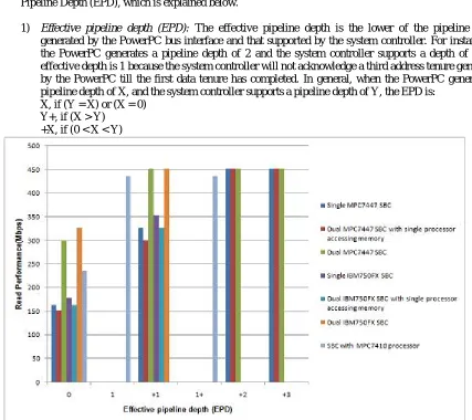
CPU pipelines, and so does the system controller. In this case, the performance depends on the Effective Pipeline Depth (EPD), which is explained below.
1) Effective pipeline depth (EPD): The effective pipeline depth is the lower of the pipeline depth generated by the PowerPC bus interface and that supported by the system controller. For instance, if the PowerPC generates a pipeline depth of 2 and the system controller supports a depth of 1, the effective depth is 1 because the system controller will not acknowledge a third address tenure generated by the PowerPC till the first data tenure has completed. In general, when the PowerPC generates a pipeline depth of X, and the system controller supports a pipeline depth of Y, the EPD is:
X, if (Y = X) or (X = 0) Y+, if (X > Y)
+X, if (0 < X < Y)
Figure 1: Read performance versus effective pipeline depth
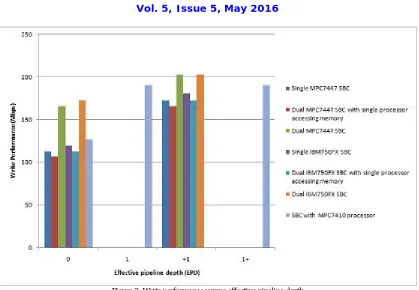
Figure 2: Write performance versus effective pipeline depth
Figure 2 shows theoretical write performance improvement on the SBCs under test
Figure 3: Copy performance versus effective pipeline depth
Figure 3 shows theoretical read performance improvement on the SBCs under test.
performance), and, if necessary and possible, optimize the application to improve pipelining. Write performance accounts for one read (store miss) and a write (cast-out), whereas “copy performance” accounts for two reads (one
load miss, one store miss) and a write (cast-out). Note that it is difficult to predict what pattern the read-write transaction mix will take, since it depends on the application and CPU system dynamics. The theoretical figures in this section, therefore, should only be taken as rough estimates; actual performance may be slightly better or worse.
2) Effect of memory interleaving: The Discovery family of controllers supports interleaving between physical banks, or between virtual banks, of memory. When interleaving is enabled, the memory controller can boost performance by hiding the activate cycles of a fresh transaction targeted to one particular bank during another (previously accessed) bank’s data cycles. In principle, a 100% occurrence of interleaving (no two successive transactions being targeted to the same physical(virtual bank) can result in full utilization of the SDRAM bus, giving maximum throughput. This is possible with both physical and virtual interleaving. Boards that use multiple physical banks provide greater scope for interleaving. Having multiple physical banks also provides more open pages, which can be leveraged to enhance performance.
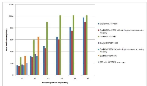
3) Read performance with ideal (100%) interleaving: Figure 4 shows, for different “effective pipeline depths”, memory read performance improvement on the SBCs under test, assuming 100% “alternate bank access” i.e. every read targets a virtual or physical bank different from that targeted by the previous read. The graph illustrates the fact that even with such an access pattern, there is no advantage if the CPU cannot generate back-to-back transactions fast enough (interleaving then never takes place). For cases where the CPU does not generate enough traffic to saturate the memory bus to its base maximum throughput (i.e. throughput with interleaving disabled), no improvement in performance is seen when compared to figure 1.
4) Key inferences from figure 4:
At low pipeline depths, when the CPU does not generate back-to-back transactions fast enough, interleaving cannot be exploited.
SBC with single processor MPC7447 and memory controller MV64360 can, with 100% interleaving, attain a peak CPU-to-memory throughput of 977Mbps, at an EPD of +5. At
higher EPDs, it can theoretically achieve the saturation throughput (at 133MHz) of 1017.3Mbps; but +5 is the maximum practical EPD for the MPC7447. SBC with dual processor MPC7447 but only single processor accessing memory lags behind the former because of the higher latency involved in a dual-CPU configuration.
SBC with dual processor MPC7447 can achieve the saturation throughput of 1017.3Mbps at an EPD of +3 itself. Note that the maximum throughput is achievable because the MPX bus supports data streaming (no idle cycle between successive data phases). Further, this is made possible because the MPX data bus arbitration is hidden, so that no clock cycles are wasted by the arbiter in switching the data bus grant between the two CPUs.
G. CPU-to-memory practical performance measurements
This section shows the practical results of performance benchmarks on the SBCs under test.
Figure 5: Measured read performance
Figure 7 shows measured read performance with stride size of 32 bytes with interleaving and page mode disabled
Figure 6: Measured write performance
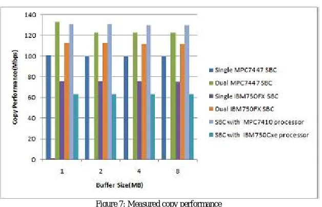
Figure 7: Measured copy performance
Figure 9 shows measured copy performance with stride size of 32 bytes with interleaving and page mode disabled
Figure 7, 8 and 9 shows the practical values of performance achieved for read, write and copy. The software tools used to measure read, write and copy performance are simple tests developed. They are referred to as memory read, memory write and memory copy respectively. The operating system used for the tests was VxWorks. Memory read starts with a buffer size of 1MB (greater than the L2 cache size), and performs successive 4-byte reads over the entire buffer size (note that all CPUs under consideration here are 32-bit CPUs). The "gap" or "stride" between successive reads is a user-defined parameter that can be specified via the console. For instance, memory read 1 reads every 4-byte element in the buffer (so that memory read over a 1MB buffer size will result in 256k read instructions being executed); memory read 2 strides 8 bytes, thus reading the first 4-byte element, the fifth 4-byte element, the ninth 4-byte element, and so on, but skipping the ones in between. memory read 4 strides 16 bytes, whereas memory read 8 strides 32 bytes. Since the PowerPC cache line size is 32 bytes,memory read 8 actually causes only one read instruction per cache-line, and this makes it ideal for measurement of main memory performance when cache is enabled and configured as write-back – because for write-write-back cache, all data reads and writes initiated by the CPU to main memory are cache-line sized (32-byte) bursts. Figure 7, 8 and 9 shows measured performance for read, write and copy for stride size of 32 bytes with interleaving and page mode disabled.
III.MEMORY-TO-MEMORY IDMA PERFORMANCE
TABLE II
Theoretical IDMA performance with interleaving and page mode disabled
SBC description 32bytes 64bytes 128bytes
Dual processor MPC7447 with controller MV64360
203.4 Mbps 387.6 Mbps 561.2 Mbps
Dual processor IBM750FX with controller MV64360
203.4 Mbps 387.6 Mbps 561.2 Mbps
Single processor IBM750CXe with controller GT64260
203.4 Mbps 280.7 Mbps 361.7 Mbps
Single processor MPC7410 with controller MPC107
218 Mbps not supported not supported
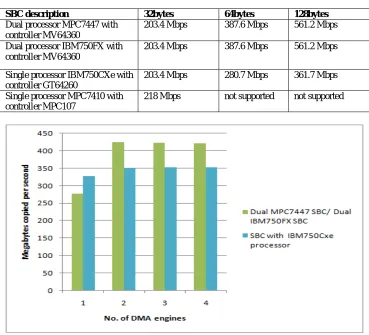
Figure 8: Measured copy performance with interleaving disabled
Figure 10 shows the measured copy performance with IDMA channels and interleaving disabled
.
Figure 9: Measured copy performance with interleaving enabled
Memory-to-memory data transfers using IDMA channels can achieve higher memory bandwidths than CPU-to memory data transfers if the IDMA controller supports burst sizes larger than 32 bytes. The CPU does not generate bursts longer than 32 bytes, and the memory controller (with page mode and interleaving disabled) on every access activates a page (RAS#), issues a command (CAS#) and after the data transfer (4-beat burst) closes (recharges) the page. But when the burst length exceeds 4, the memory controller drives a fresh command (CAS#) cycle after every 4 data beats, without closing the page. This offers significantly higher performance, especially on the SBCs having DDR memory where the dual-data rate capability of DDR memory is exploited. Therefore the SBC with processor IBM750FX and SBC with processor MPC7447 and memory controller MV64360 that supports DDR memory and increasing number of IDMA channels shows a improved performance.
IV.PCI-TO-MEMORY PERFORMANCE
This section deals with read and write transactions generated by an external PCI master, targeted to the host memory of the SBC. The target board has a memory-mapped inward window to memory in the PCI configuration space. PCI performance has been measured on the SBC with IBM750Cxe and the SBCs with IBM750FX and MPC7447 PowerPC processors in 32-bit, 33MHz mode using a Catalyst TA660 PCI analyzer/exerciser as the bus master.
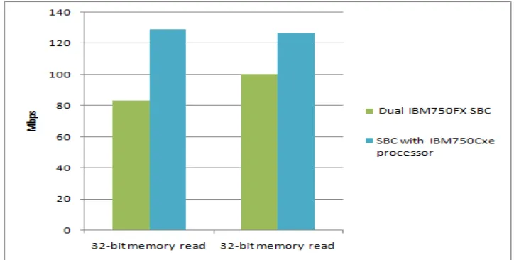
Figure 10: Measured PCI performance with read size of 256 bytes, write size of 400 bytes
It is seen from figure 12 that in both the read size of 256 bytes and 400 bytes, the performance of the SBC with processor IBM750Cxe that uses memory controller GT64260 is more than the SBC with dual processor IBM750FX that uses memory controller MV64360. This is because of the lower PCI to memory latency of the former than the later.
V. DUAL-CPU PERFORMANCE WITH CACHE COHERENCY
TABLE III
Performance result on 8MB cache coherent region
SBC description Read
performance (Mbps) on CPU0
Write performance (Mbps) on CPU1 Dual processor IBM750FX with
controller MV64360
75 75
Dual processor MPC7447 with controller MV64360
376 95
Table III shows the read and write performance comparison between two SBCs incorporating dual CPU having same memory controller but working with two different front side bus protocol. Since the MPX bus supports the "data intervention" feature, the SBC having dual MPC7447 processors is expected to perform way better than the SBC having dual IBM750FX processors using 60X bus in the front-side bus in this regard. Table III shows results observed for a buffer size of 8MB. Obviously, the SBC with two MPC7447 processors sees a high read-performance on CPU0 despite the fact that every transaction results in a snoop hit on CPU1. On the other SBC having two IBM750FX processors, every cache-line read on CPU0 has to wait for a cast-out from CPU1 to complete; since a write from CPU1 and a read from CPU0 are thus inseparably tied together, both see the same performance.
VI.RESULT AND DISCUSSION
For a buffer size of 1MB, SBC with processor MPC7410 and memory controller MPC107 shows significantly higher performance than the rest, but this is because it has 1MB of L2 cache. This is evident from figure 7 and 8.
For higher buffer sizes, SBC with processor MPC7447 and memory controller MV64360 performs better than the rest because of superior pipelining depth.
On SBC with dual processor MPC7447 and memory controller MV64360, the performance touches 75% of the maximum memory performance possible, just on account of intense pipelining on the bus.
SBC with single processor IBM750FX achieves 306MBps, which is 90% of the maximum theoretical performance at a pipeline depth of +1. SBC with dual processor IBM750FX achieves 434MBps, which is very close to the theoretical maximum of 452MBps at an EPD of +1.
SBC with processor IBM750Cxe and memory controller GT64260 shows no significant performance improvement this is because of the inability of the CPU to pipeline reads.
SBC with processor MPC7410 and memory controller MPC107 achieves above 90% of the theoretical maximum performance of 436MBps at an EPD of 1.
The copy performance increases with the increase in number of IDMA engines as seen from figure 10 and 11.
VII. CONCLUSION
another 64kB chunk of memory, and so on. Considering the performance analysis and results obtained, it is clear that the SBC with processor Motorola PowerPC MPC7447 and memory controller MV64360 of Marvell Technology stands above the rest in terms of memory performance potential. The key is to be able to exploit the potential by appropriate system settings and software tuning.
A. Cache performance
The SBC with processor Motorola PowerPC MPC7447 and memory controller MV64360 of Marvell Technology provides superior L1 and L2 cache performance (except at 1MB) because of the 1GHz core frequency and latest generation PowerPC. The SBC with processor IBM PowerPC IBM750FX and memory controller MV64360 of Marvell Technology is marginally better than the SBC with processor IBM PowerPC IBM750CXe and memory controller GT64260 of Marvell Technology in terms of cache performance. The SBC with processor MPC7410 and memory controller MPC107, however, has larger L2 cache (1MB), because of which it exhibits superior performance at 1MB. For applications that utilize 512kB or less memory, the SBC with processor Motorola PowerPC MPC7447 and memory controller MV64360 will offer the best performance.
B. CPU-to-memory performance
The SBC with processor Motorola PowerPC MPC7447 and memory controller MV64360 of Marvell Technology has the highest performance potential (can approach 1GBps of read bandwidth) here, but it is very important that the application takes advantage of FSB pipelining. Otherwise, the performance could be worse than the other SBCs. The SBC having dual-CPU of IBM750FX, though, can achieve higher memory performance than the SBC with processor Motorola MPC7410 and memory controller MPC107 when both CPUs simultaneously access memory.
C. IDMA performance
The DDR advantage makes both the SBC with processor Motorola PowerPC MPC7447 and IBM PowerPC IBM750FX and memory controller MV64360 of Marvell Technology capable of excellent IDMA copy performances; however, the unique design of the memory controller MV64360 of Discovery-II family of Marvell Technology, which is optimized for multiple requesting units accessing memory, necessitates the usage of multiple IDMA channels in parallel in order that the throughput exceeds that of SBC with processor IBM750Cxe and memory controller GT64260 of Marvell Technology.
D. PCI-to-memory performance
SBC with processor IBM750Cxe and memory controller GT64260 of Marvell Technology offers the best read-performance numbers here, because of the relatively lower latencies between PCI and SDRAM. The SBCs with processor Motorola PowerPC MPC7447 and IBM PowerPC IBM750FX lag behind a bit; however, when there are multiple PCI agents simultaneously trying to access the host memory, the advantage of DDR will come through and help increase overall PCI throughput.
E. System performance
From a system perspective, when there are multiple units accessing memory simultaneously, the the SBCs with processor Motorola PowerPC MPC7447 and IBM PowerPC IBM750FX have an edge over the rest. The Discovery family of system controller also supports multiple Ethernet controllers and communication ports which will, in practice, continuously access memory. In this real-world scenario, the Discovery-II family of system controller promises better overall memory performance.
F. Dual-CPU performance with cache-coherency
REFERENCES
[1] P. Heidelberger, S. S. Lavenberg, “Computer Performance Evaluation Methodology”, IEEE Transactions on Computers (Volume:C-33 , Issue: 12 )
[2] C Roth, F Levine, Power PC Performance Monitor Evolution, Performance, Computing, and Communications Conference, 1997. IPCCC 1997., IEEE International
[3] C Roth, F Levine, “A programmer’s view of performance monitoring in the PowerPC microprocessor”, IBM Journal of research and development-special issue: performance analysis and its impact on design, Vol 41, issue 3, May 1997
[4] M. Snyder and M. Denman, "The Design of the PowerPC 604e Microprocessor", Proceedings of COMPCON \'96, pp. 126-131, 1996 [5] H. Dwyer , R. Heisch , F. Levine and E. Welbon, "Technique for Speculatively Sampling Performance Parameters", IBM Technical Disclosure
Bulletin, vol. 37, no. 9, pp. 589-592, 94
[6] C. Roth , F. Levine and E. Welbon, "Performance Monitoring on the PowerPC 604 Microprocessor", Proceedings of ICCD \'95, pp. 212-215, 1995
[7] Nitin Chaturvedi, S Gurunarayanan, “Study of various factors affecting performance of multi-core processors, IJDPS, Vol 4, No. 4, July 2013 [8] Rinki Kanger, Parikshit Singla, “Performance Evaluation of CPU Scheduling Technique with an Efficient Genetic Algorithm”, IJCST Vol 4,
Issue , July – Sept 2013
[9] F. Levine, "Generic Performance Monitor Interface Approach", IBM technical Disclosure Bulletin, vol. 39, no. 8, pp. 65-68, 96 [10] MPC7447 User Manual, Rev 2.2, October 2002, Motorola.
[11] IBM750CXe User Manual, V1.1, May 2002, IBM. [12] IBM750FX User Manual, V1.0.1, April 2003, IBM [13] MPC7410 user’s manual, Rev 0, Oct 2000, Motorola.
[14] MPC107 user’s manual, Rev 0, Nov 2000,} MPC107 user’s manual, Rev 0, Nov 2000, Motorola. [15] JEDEC DDR SDRAM specification, JEDEC DDR SDRAM specification.
[16] DDR SDRAM user manual, DDR SDRAM user manual, Hynix.
[17] Samsung 512Mb DDR SDRAM datasheet, Samsung 512Mb DDR SDRAM datasheet, Hynix. [18] SDRAM user manual, SDRAM user manual, Elpida.