High Step-Up Forward Flyback Converter
with Nondissipative Snubber for Solar Energy
Application
Divya Dileep Kumar1, Maheswaran. K2
PG Student [PED], Dept. of EEE, Nehru College of Engineering and Research Centre, Thrissur, Kerala, India1
Assistant Professor, Dept. of EEE, Nehru College of Engineering and Research Centre, Thrissur, Kerala, India2
ABSTRACT: A high step-up forward flyback converter with nondissipative snubber for solar energy application is introduced here. High gain DC/DC converters are the key part of renewable energy systems .The designing of high gain DC/DC converters is imposed by severe demands. It produces high step-up voltage gain by using a forward flyback converter. The energy in the coupled inductor leakage inductance can be recycled via a nondissipative snubber on the primary side. It consists of a combination of forward and flyback converter on the secondary side. It is a hybrid type of forward and flyback converter, sharing the transformer for increasing the utilization factor. By stacking the outputs of them, extremely high voltage gain can be obtained with small volume and high efficiency even with a galvanic isolation. The separated secondary windings in low turn-ratio reduce the voltage stress of the secondary rectifiers, contributing to achievement of high efficiency. Here presents a high step-up topology employing a series connected forward flyback converter, which has a series connected output for high boosting voltage-transfer gain. A MATLAB/Simulink model of the Photo Voltaic (PV) system using Maximum Power Point Tracking (MPPT) has been implimented along with a DC/DC hardware prototype.
KEYWORDS: PV Model Parameter, Insolation, Dual-Voltage Doubler Circuits, Voltage Gain, Nondissipative snubber, Forward-Flyback Converter, MPPT Technique.
I.INTRODUCTION
One of the primary objectives of the forward flyback converter is to achive a high step up voltage gain, it make the converter for the utilisation of Photo Voltaic applications. In day by day our source of energy like oil, gas and water is decreasing, so we have to use the never ending energy like wind and solar. For using this type of energy we have to modify the existing circuitry or model suitable for this type of inputs. Such a model of converter system is introduced here. This converter input is provided by using a solar sell. In this new design a nondissipative snubber, is utilized to reduce voltage stress on the switch and a forward flyback converter, which transfer the maximum power to the load.
In order to obtain high efficiency, a high step-up forward flyback converter with a nondissipative snubber is presented. For this, a forward and a flyback converter are fabricated on the secondary side to achieve high voltage gain.
II.LITERATURE SURVEY
Nondissipative LC turn-off snubber reduces the voltage stress on a switching transistor, which is caused by the energy stored in the transformer leakage inductance. The LC snubber has the advantage over the conventional RCsnubber, in that the power dissipation by snubber resistor is eliminated [1].Developments of a photovoltaic array maximum power point tracking techniques are discussed. It describes many different techniques for maximum power point tracking of photovoltaic (PV) array. It shows that 19 distinct methods have been introduced with many variations on implementation [2]. Develop a simulation model of PV array [4], [5]. Nonisolated converters for high step-up applications are used with coupled inductors [8], [14] to obtain high step-up gain and to recycle leakage energy in order to improve efficiency. However, the high step-up gain of nonisolated converters cannot satisfy the requirements of the galvanic isolation standards. Thus, some isolated high step-up converters have been proposed. These converters can be used with coupled inductors integrated with isolated transformers [10], voltage multipliers [11], coupled inductors integrated with voltage multipliers [12], primary-parallel–secondary-series structures integrated with coupled inductors [3]. The proposed topology has high step up voltage gain and low stress on switching device.
III.ISOLATED HIGH STEP-UP DC-DC CONVERTER
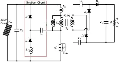
Isolation means existence of an electrical barrier between the input and output of the DC-DC converter. Fig.1 shows the existing step-up DC-DC converter.
Fig. 1 Isolated high step-up dc–dc converter (Existing System)
This converter consists of the voltage of the solar panel VPV, an input capacitor Cin, snubber diodes D1 and D2, a snubber inductor L1, a snubber capacitor C1, a coupled inductor T1, a main switch Q1, two step-up capacitors C2 and C3, two step-up diodes D3 and D4, an output diode Do, an output capacitor Co and an output load R. This system voltage
gain is 8. But the modified system voltage gain is 9. The modified system is shown in Fig.2.
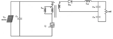
Fig. 2 Isolated high step-up dc–dc converter (Modified System)
Dfb, the flyback diode; Dff, the freewheeling diode; Cfw, the forward capacitor; Cfb, the flyback capacitor and Lout , the
output inductor. This converter has high voltage gain because of stacking the outputs of forward and flyback converter. The separate secondary winding reduces the voltage ratings of rectifying diodes. The energy stored in the nondissipative snubber capacitor is recycled to the voltage of the solar panel VPV and the input capacitor Cin, thereby improving the system efficiency. Moreover, Maximum Power Point Tracking (MPPT) is important for solar energy applications. Here, the Perturb and Observe (P&O) algorithm is utilized to achieve an MPPT function for solar energy conversion applications.
IV.OPERATING PRINCIPLES OF THE PROPOSED CONVERTER
The proposed converter has seven operating modes as shown in Fig. 3 to Fig. 9.
Mode I: In this mode the diode D1 is reverse biased. The switch Q is ON, current flows to the magnetizing inductance
and the primary winding of transformer. The primary current is transferred to the secondary coil of the forward converter via the magnetic linkage. In this mode the capacitor C1 releases energy to inductor L1.
Fig. 3 Equivalent circuit of mode I
Mode II: The operating principle of the main circuit is same as mode I. The only difference is in the snubber circuit as shown in Fig. 4. The energy of inductor L1 is recycled mainly to the load.
Fig. 4 Equivalent circuit of mode II
Mode III: The switch Q is ON as shown in Fig. 5. The energy stored in L1 is zero so the snubber circuit is totally
inactive. The main operating principle is same as mode II.
Fig. 5 Equivalent circuit of mode III
Mode IV: In this mode the switch Q, diode D2 and diode Dfwis turned OFF as shown in Fig. 6. The leakage inductance
current iLK, charges the snubber capacitor C1 and parasitic capacitor of Q. The energy stored in Lout is transferred to load
Fig. 6 Equivalent circuit of mode IV
Mode V: In this mode the operating principle is same as mode IV. The stored energy in C1is released to Vpv,Cin and to
the winding of flyback converter. Thus the leakage energy can be recycled.
Fig. 7 Equivalent circuit of mode V
Mode VI: The leakage inductor current become zero. The magnetizing inductance Lm releases energy to the load via Dfb. In this mode the diode Dff is turn OFF. In this mode the energy stored in Lmis only supplied to the load.
Fig. 8 Equivalent circuit of mode VI
Mode VII: The transformer of the forward flyback converter is demagnetized completely during this period and the output voltage is maintained by the discharging of the output capacitor. All the rectifier diodes are turn OFF as shown in Fig. 9.
V:MATLAB/SIMULINK SIMULATION AND HARDWARE MODEL OF PV INTEGRATED DC-DC CONVERTER
In the simulation model the input voltage is 30V DC and gets the output as 274V DC. Fig. 10 shows the simulation model. The gate pulse given to the switch is using the P&O MPPT technique.
Fig. 10 Matlab simulation model
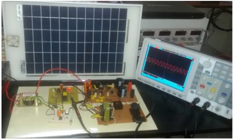
The experimental setup is shown in Fig. 11. It consists of a controller board, driver board and the forward flyback converter circuit board design.
VI. RESULT AND DISCUSSION
Fig. 11 shows the input and output waveforms of the converter simulation model. It shows that input voltage is 30V and obtains the output as 274V DC.
Fig. 12 Input and output waveforms
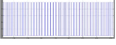
Fig. 12 shows the gate pulse given to the switch using MPPT technique. This gate pulse is obtained in the matlab simulation model. In the hardware design this pulse is generated using ATMEGA16 microcontroller.
Fig. 13 Gate pulse
VII.CONCLUSION
PV module has been developed and verified using MATLAB/Simulink. The simulation model of PV is developed using the mathematical equations and basic math functions. There is an isolated coupled-inductor integrated DC-DC converter with a nondissipative snubber. The proposed converter topology has larger voltage gain as that of existing converter topology. It consists of a combination of forward and flyback converter on the secondary side. By stacking the outputs of them, extremely high voltage gain can be obtained. The energy in the coupled inductor leakage inductance can be recycled via a nondissipative snubber on the primary side. The separated secondary windings in low turn-ratio reduce the voltage stress of the secondary rectifiers, contributing to achievement of high efficiency. The detailed simulation diagrams and the corresponding waveforms have been provided. The result shows that high stepup voltage gain and high efficiency are achieved. A hardware prototype of DC-DC converter is also developed.
REFERENCES
[2] Trishan Esram and Patrick L. Chapman, “Comparison of Photovoltaic Array Maximum Power Point Tracking Techniques”, IEEE Transactions on Energy Conversion, vol. 22, no. 2, pp. 439–449, Jun. 2007.
[3] Wuhua Li, Jun Liu, Jiande Wu and Xiangning He, “Design and Analysis of Isolated ZVT Boost Converters for High-Efficiency and High-Step-Up Applications”, IEEE Transactions on Power Electronics, vol. 22, no. 6, pp. 2363–2374, Nov. 2007.
[4] Marcelo Gradella Villalva, Jonas Rafael Gazoli and Ernesto Ruppert Filho, “Comprehensive Approach to Modeling and Simulation of Photovoltaic Arrays”, IEEE Transactions on Power Electronics, vol. 24, no.5, pp. 1198-1208, May 2009.
[5] Michael E. Ropp and Sigifredo Gonzalez, “Development of a MATLAB/Simulink Model of a Single-Phase Grid-Connected Photovoltaic System”, IEEE Transactions on Energy Conversion, vol.24, no.1, pp.1-8, May 2009.
[6] Dong Wang, Xiangning He and Jianjiang Shi, “Design and Analysis of an Interleaved Flyback–Forward Boost Converter With Current Auto Balance Characteristic”, IEEE Transactions on Power Electronics, vol. 25, no. 2, pp. 489–498, Feb. 2010.
[7] Giovanni Petrone, Giovanni Spagnuolo and Massimo Vitelli, “A Multivariable Perturb-and-Observe Maximum Power Point Tracking Technique Applied to a Single Stage Photovoltaic Inverter”, IEEE Transaction on Industrial Electronics, vol. 58, no. 1, pp. 76–84, Jan. 2011. [8] Suman Dwari and Leila Parsa, “An Efficient High-Step-Up Interleaved DC–DC Converter With a Common Active Clamp”, IEEE Transactions
on Power Electronics, vol. 26, no. 1, pp. 66–78, Jan. 2011.
[9] K. I. Hwu, Y. T. Yau and Li-Ling Lee, “Powering LED Using High-Efficiency SR Flyback Converter”, IEEE Transaction on Industrial Applications, vol. 47, no. 1, pp. 376–386, Jan./Feb. 2011.
[10] Bor-Ren Lin, Jia-Yu Dong and Jyun-Ji Chen, “Analysis and Implementation of a ZVS/ZCS DC–DC Switching Converter With Voltage Step-Up”, IEEE Transaction on Industrial Electronics, vol. 58, no. 7, pp. 2962–2971, Jul. 2011.
[11] Giorgio Spiazzi, Paolo Mattavelli and Alessandro Costabeber, “High Step-Up Ratio Flyback Converter With Active Clamp and Voltage Multiplier”, IEEE Transactions on Power Electronics, vol. 26, no. 11, pp. 3205–3214, Nov. 2011.
[12] Hyun-Lark Do, “Improved ZVS DC–DC converter with a high voltage gain and a ripple-free input current”, IEEE Transactions on Circuits Systems, vol. 59, no. 4, pp. 846–853, Apr. 2012.
[13] Shih-Ming Chen, Tsorng-Juu Liang, Lung-Sheng Yang and Jiann-Fuh Chen, “A Safety Enhanced, High Step-Up DC–DC Converter for AC Photovoltaic Module Application”, IEEE Transactions on Power Electronics, vol.27, no. 4, April 2012.