Available online: https://edupediapublications.org/journals/index.php/IJR/ P a g e | 1479
Implementation of PPA-Brent Kung Adder For
Computing Application
G.CHANDRASEKHAR *, MOHAMMAD TAJ
G.Chandrasekhar
,
M-Tech (VLSI), ECE Department Eluru College of Engineering and
Technology, JNTUK A
.P
Mohammad Taj ,
Assistant Professor
,
ECE Department Eluru College of Engineering and
Technology, JNTUK A.P
ABSTRACT
In this paper, the implementation of residue number system reverse converters
based on Brent Kung adders is analyzed. The parallel prefix adder provides high speed and
reduced delay arithmetic operations but it is not widely used since it suffers from high
power consumption. Hence, a Brent Kung adder component is presented to perform fast
modulo addition in Residue Number System reverse conversion. The proposed components
are not only results in fast arithmetic operation and it also highly reduced the hardware
complexity since it requires fewer amount of logic elements. In this work, the proposed
components are implemented in different module sets reverse converter designs and the
performances are compared for different values of n.
KEYWORDS:
Digital arithmetic, Brent kung adder , parallel-prefix adder, residue number
system (RNS), reverse converter.
INTRODUCTION
The Residue Number System plays a
significant role in the battery based and
portable devices because of its low power
features and its competitive delay. The
Residue number system reverse converter is
designed with parallel prefix addition by
using new components methodology for
higher speed operation. The RNS consists
of two main components forward and the
reverse converter that are integrated with
the existing digital system. The forward
converter performs
the operation of
converting the binary number to the modulo
number whereas the reverse converter
performs
the
operation
of
reverse
converting the modulo number to the binary
number which is the hard and time
consuming process compared with the
Available online: https://edupediapublications.org/journals/index.php/IJR/ P a g e | 1480
concepts such as 1)RNS definition with
pr
operties and theirapplications,2)consideration of modulo set
selection,3)design
of
forward
converter,4)moduloarithmetic
units,5)design of reverse converter are
discussed.
The voltage over scaling (VOS) technique is
applied to the residue number system to
achieve high energy efficiency. The VOS
technique introduces soft errors which
degrades the performance of the system. To
overcome these soft errors a new technique
is implemented called joint RNS-RPR
(JRR) which is the combination of RNS and
the reduced precision redundancy. This
method provides the advantage of satisfying
the basic properties of RNS includes shorter
critical path, reduced complexity and low
power. New architectures are presented for
the moduli set (2n-1,2n, 2n+1) for the
conversion from the residue to the binary
equivalents. Here the speed and the cost are
major concern.
Distributed arithmetic principles are used to
perform the inner product computation. The
input data which are in the residue domain
which are encoded using the Thermometer
code format and the outputs are encoded
using the one hot code format. Compared to
the conventional method which used Binary
code format, the proposed system which
achieves higher operating speed. The
residue number system which provides
carry free addition and fully arithmetic
operation, for several applications such as
digital signal processing and cryptography.
In this brief, we present a comprehensive
method which uses the parallel prefix adder in
selected position, thereby using the shift
operation on one bit left to design a multiplier
on the same design module to achieve a fast
reverse converter design. The usage on parallel
prefix structure in the design leads to higher
speed in operation meanwhile it increases the
area and power consumption.Inorder to
compensate the tradeoff between the speed, area
and power consumption, a novel specific Brent
Kung parallel prefix based adder components
are used to design the reverse converter. These
Brent Kung design which provides the
significant reduction in the power delay product
(PDP) metric and leads to considerable
improvements in the area time² product (AT²) in
comparison with the traditional converters
without using parallel prefix adders
PARALLEL PREFIX STRUCTURE
The Residue number system mainly composed
of three main parts such as, forward converter,
modulo arithmetic units and reverse converter.
On comparing with the other parts the reverse
converter design is a complex and no modular
structure. So more attention is needed in
Available online: https://edupediapublications.org/journals/index.php/IJR/ P a g e | 1481 preventing the slow operation and compromises
the benefits of the RNS.The parallel prefix
structure helps to achieve the faster operation in
the reverse converter design but causes
increased power consumption. In the existing
system the novel specific Brent Kung parallel
prefix adder based components are used to
replace the existing components there by
reducing the power consumption and getting
faster operation.
A. Parallel Prefix Block.
Fig.1 Basic Parallel prefix structure
The Parallel prefix structure consists of three
main blocks, they are preprocessing block,
prefix carry tree and post processing block. The
parallel prefix adder operation begins with
preprocessing stage by generating the Generate
(Gi) and Propagate (Pi) equation[1]&[3].The
prefix carry tree get proceeded with the
previous block signal to yield all carry bit signal
and these stage contains three logic complex
cells such as Black cell, Gray cell and Buffer
cell. Black cell compute both the propagate
(P(i,j)) and generate (G(i,j)) by using the
equation[3]&[4].The Gray cell executes only
the generate(G(i,j)).The carry bits generated in
the second stage get passed to the post
processing block thereby generating the sum
using the equation[5].The block diagram is
shown in the Fig1.
The Brent Kung adder prefix structure:
Gm:n=An AND Bn
(1) G0 =Cin
(2) Pm:n=An XOR Bn
(3) P0=0
(4) Gm:n=Gn:k OR Pn:k AND Gk-1:n
(5)
Pm:n=Pn:k AND Pk-1:j
(6) Sn =Pn XOR Cin
Available online: https://edupediapublications.org/journals/index.php/IJR/ P a g e | 1482
It is employed to achieve the higher speed with
reduced power consumption. On comparing
with the other parallel prefix adder structure
the BK adder is chosen mainly for
minimum fan-out and should be higher
speed in operation than others.Fig.2shows
the example BK adder prefix structure
which uses the three basic cells in the prefix
structure. These structure is elaborated for
the proposed design having the modulo
addition of (4n+1) for n=5.
Fig.2:4-bit BK adder prefix structure
B.HRPX Structure :( Brent Kung Regular Parallel prefix XOR/OR adder component)
Fig.3 HRPX Structure using BK prefix network
Fig.3 shows HRPX Structure. The regular parallel prefix adder is used to do the first part of addition and
the simplified RCA logic is used to do the second part where the corresponding bits of the operand are
Available online: https://edupediapublications.org/journals/index.php/IJR/ P a g e | 1483 Full adder can be designed with XOR/OR
gates because of the constant operand. In these
reverse converters design the carry chain is not
needed and can be ignored. For most modulo
sets (2ⁿ-1) addition is a necessary operation. The End around Carry (EAC) for (2ⁿ-1) addition is
represented with two zero, but for the reverse
converter design one zero representation is
required. To correct these zero representation
problem, a detector circuit was employed in the
design but it incorporates additional delay. So,
the Binary to excess one converter (BEC) is
used to solve the double zero representation
issue.
NEW PARALLEL-PREFIX-BASED COMPONENTS
The HMPE Structure consists of two parts:
Regular prefix adder and the Modified Excess
One unit. The first two operands are added
using the parallel prefix adder and the result is
conditionally incremented based on the control
signal generated by the prefix structure to assure
the single zero representation. The below figure
shows HMPE Structure.
Fig.4: HMPE Structure
Modified Excess One unit Description:
Available online: https://edupediapublications.org/journals/index.php/IJR/ P a g e | 1484
Fig.5 shows the Modified Excess One unit
circuit diagram. The result generated by the
prefix structure is conditionally incremented
by this unit based on the control signal
generated by the parallel prefix adder.
The reverse converter design is
implemented for (4n+1) modulo addition
(n=5) designing the adder and also the
multiplier by using the same adder design
without using any parallel prefix multiplier
structure for designing multiplier.
In this design, the adder design is
implemented by using the Kogge Stone adder
parallel prefix structure. Here the first two
operands are added by using the prefix adder
preprocessing stage thereby generating the
propagate and generate equation. The first
stage processed signal get passed to the next
stage called the prefix carry tree, this stage
again computes the generate and propagate
equation by using the previous output and all
the logic cells employed in the Kogge Stone
adder network. These processed signals are
passed to the post processing block.
The simulation process has been carried
out for different levels of abstraction. The
code has been written in Verilog hardware
description language. The top module has
been synthesized and simulated in
Xilinx ISEDesign Suite 12.3 and the corresponding delay
calculations have been noted. By using Kogge
Stone Adder the delay and area was reduced.
Simulation results are shown in fig 6and 7. RTL
Schematic diagrams are shown in fig 8 and 9.The
design was implemented in Spartan-3E kit.
Fig.6: Simulation result of HMPE-BK Adder Parallel Prefix Structure
Available online: https://edupediapublications.org/journals/index.php/IJR/ P a g e | 1485
5.2: RTL (Register Transfer Level) schematic diagrams:
Fig.8: RTL Schematic of HMPE- BK Adder Parallel Prefix Structure
Fig.9: RTL Schematic of HMPE- KS Adder Parallel Prefix Structure
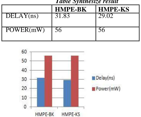
5.3: Synthesize Result:
Table shows the synthesize result for using Xilinx project navigator for device xc3s400-4pq208
Table Synthesize result
HMPE-BK HMPE-KS
DELAY(ns) 31.83 29.02
POWER(mW) 56 56
Available online: https://edupediapublications.org/journals/index.php/IJR/ P a g e | 1486
CONCLUSION
This proposed work presents Brent Kung
based adder components that give better tradeoff
in area and delay are thus exhibited to design
reverse converters. A methodology is described
to design reverse converters depending on
various
types
of
prefix
adders.
These
components are particularly designed for
reverse converters. Implementation results gives
that the reverse converters depending on the
suggested work significantly decreases the area
and delay when contrasted and the original
converters, which don't utilize any
parallel-prefix adders. Future work includes the
extension of the bit size and to construct an
efficient reverse converter.
REFERENCES
[1] Omondi and B. Premkumar, Residue Number Systems: Theory and
Implementations. London, U.K.: Imperial College Press, 2007.
[2] B. Parhami, Computer Arithmetic:
Algorithms and Hardware Designs, 2nd ed., New York, NY, USA: Oxford Univ. Press, 2010.
[3] J. Chen and J. Hu, “Energy-efficient digital signal processing via voltageover scaling-based residue number system,” IEEE Trans. Very Large Scale Integr. (VLSI) Syst., vol. 21, no. 7, pp. 1322–1332, Jul. 2013. [4] C. H. Vun, A. B. Premkumar, and W.
Zhang, “A new RNS based DA approach for inner product computation,” IEEE Trans. Circuits Syst. I, Reg. Papers, vol. 60, no. 8, pp. 2139–2152, Aug. 2013.
[5] S. Antão and L. Sousa, “The CRNS framework and its application to programmable and reconfigurable
cryptography,” ACM Trans. Archit. Code Optim., vol. 9, no. 4, p. 33, Jan. 2013. [6] A. S. Molahosseini, S. Sorouri, and A. A. E.
Zarandi, “Research challenges in next-generation residue number system