Abstract
JAEGER, DAVID. Electron Emission from Low Dimensional Structures. (Under the direction of Dr. John J. Hren).
A fundamental technological driving force is the search for simpler, more efficient and economical means of accomplishing a task. Nano-scale materials are seen as a means to efficiently emit electrons from a solid under the action of an electric field. The drive to smaller scales is also seen as a means to efficiently and simply produce devices. A thorough understanding of the characteristics of such materials is needed to understand and fully exploit these nano-materials when used as field enhanced electron emitters and efficiently process the devices.
The focus of this work was to investigate the effects that morphology, geometry and size can have on the electron emission characteristics of vacuum field emission cathodes. Deviations in surface structure and material strongly impact cathode reliability and performance due to the effect that these deviations have on the local surface electric field. Deterministically coating the cathode surface with material can positively impact cathode reliability and performance by manipulating surface morphology, band structure, thermal conductivity, and surface stability.
was analyzed. Effects of dimensionality and quantization of the surface electron gas on vacuum field emission was studied and a model of the emission process was developed.
ii
Biography
David Jaeger was born in Kingston, NY on the 20th of January 1971. In 1982 he moved to Raleigh, NC with his family. He began his undergraduate studies at North Carolina State University in 1989 graduating with a Bachelor of Science in Physics. He later returned to North Carolina State University to pursue graduate studies under the direction of Professor John Hren, receiving a Masters degree in Materials Science and Engineering and remaining to pursue a Doctoral degree in Materials Science and Engineering.
iii
Acknowledgements
I would like to thank Dr. John Hren for the guidance, assistance and many discussions we have had and for agreeing to be my thesis adviser. Dr. Victor Zhirnov’s passion and zeal for science and the unknown have been a constant inspiration to me and for this alone I wish to thank him. I thank Dr. Olga Shenderova and the International Technology Corporation for giving me the opportunity to work with them and broaden my horizons. I thank Dr. Gerald Iafrate for taking the time to serve as on my committee and agreeing to evaluate and aid in the development of my research.
iv
Table Of Contents
List Of Figures... vii
List Of Tables ... xii
Chapter 1. Introduction... 1
1.1. Motivation/Overview of Dissertation ... 1
1.2. Quantum Tunneling Formalism... 2
1.3. Field Emission Formalism ... 5
1.4. Field Enhancement ... 7
1.5. Material effects ... 8
1.6. Thermal effects ... 9
1.7. Field Emission Applications... 10
1.8. Fabrication of Field Emitters ... 10
1.9. Summary ... 11
1.10. References... 12
Chapter 2. Local electrostatic effects of surface structure on field emission: Metal on metal composite cathodes ... 18
2.1. Abstract ... 19
2.2. Introduction... 19
2.3. Simulation and Method... 22
2.4. Results and Discussion ... 24
2.4.1. Idealized Single Tip Field Enhancement Effects... 24
2.4.2. Multistage Field Enhancement Effects ... 27
v
2.5. Conclusions... 32
2.6. References... 33
Chapter 3. Electrostatic effects of conformal and isolated diamond nanodots on field emission... 48
3.1. Abstract ... 49
3.2. Introduction... 49
3.3. Experimental Input ... 51
3.4. Numerical Method ... 52
3.5. Results and Discussion ... 52
3.6. Conclusions... 55
3.7. Acknowledgements... 56
3.8. References... 56
Chapter 4. Field Emission Device with Back-Gated Structure ... 64
4.1. Abstract ... 65
4.2. Introduction... 65
4.3. Experiments ... 68
4.3.1. Fabrication of the back-gated device structure ... 68
4.3.2. Cathode-Gate Model: Cylinder-Plane geometry... 69
4.3.3. Simulation Setup ... 71
4.4. Results and Discussion ... 74
4.5. Conclusions... 76
4.6. Acknowledgements... 77
4.7. References... 78
Chapter 5. Cold Field Electron Emission from 0D, 1D And 2D Electron Gases ... 87
vi
5.2. Introduction... 88
5.3. Tunneling Equations ... 89
5.4. Results and Discussion ... 95
5.5. Conclusions... 99
5.6. References... 99
Chapter 6. Summary ... 110
6.1. Geometric electrostatic field effects on field emission... 110
6.2. Dimensionality effects on field emission... 111
6.3. Suggested Future Work ... 111
vii
List Of Figures
1 Introduction
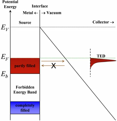
1 Conventional Fowler Nordheim emission from the partially filled conduction band of a metal cathode source into a collector through a triangular barrier potential. Current from the collector to the source is considered negligible. Electron emission is peaked near the Fermi level as shown in the schematic TED. ... 16 2 Temperature along the axis of an emitter for times 1,2,3,4; where
1 2 3 4
t < < <t t t . ... 17 2 Local electrostatic effects of surface structure on field emission: Metal on metal
composite cathodes
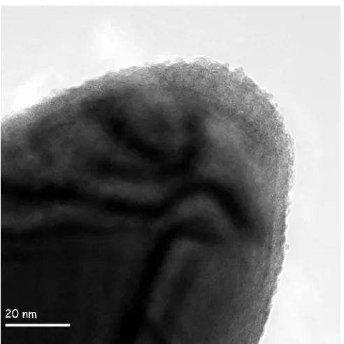
1 Planar diode geometry with ellipsoidal needle, appropriate boundary conditions approximating the experimental domain modeled and geometrical parameters. ... 38 2 HRTEM profile of an electrochemically etched Mo needle exhibiting a
nonhomogeneous profile with many surface features. ... 39 3 Field enhancement factors versus aspect ratio for ellipsoidal emitters using
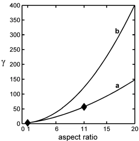
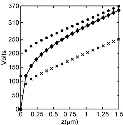
numeric and analytical methods. (a) exact analytic expression of Eq. (3c), (b) a common experimental approximation, γ ≈h r+2, and (diamonds) the FiEM result. ... 40 4 Potential normal to the ellipsoidal needle apex calculated using several
methods. (solid line) the FiEM numeric approach, (diamonds) the exact analytic formula Eq. (3a), (crosses) an approximate form of the potential given by Eq. (4a), and (circles) the modified formula of Eq. (4a) given by Eq. (4b). ... 41 5 Field enhancement across the emitter surface for a two stage composite needle.
(squares) a base needle with rc = 200nm, (diamonds) a protrusion with rc = 3nm on the surface of the base needle, and (circles) a protrusion with rc = 0.625nm on the surface of the base needle. ... 42 6 Percent error between the MSFE model and numerical results using the Finite
Element Method for various types of idealized inhomogeneities on elliptic and spherical needle substrates. (a) spherical particle embedded on spherical substrate, (b) ellipsoidal particle embedded on spherical substrate, (c) spherical particle embedded on ellipsoidal substrate, (d) ellipsoidal particle embedded on ellipsoidal substrate. ... 43 7 Field magnification values as a function of the number of substructures
viii
8 Potential profile of a composite metal needle using FiEM numeric results. Applied anode voltages of (a) 0V, (b) 100V, (c) 200V, (d) 300V, (e) 400V, (f) 500V, (g) 600V, and (h) 700V. ... 45 9 HRTEM image of the simulated needle. ... 46 10 The geometric approximation of Figure 9 and the resultant field distribution... 47 3 Electrostatic effects of conformal and isolated diamond nanodots on field
emission
Figure 1. Field distribution near the apex of a metal insulator composite needle exhibits behavior strongly dissimilar to that experienced by a wholly metal composite needle; particle radius is 5nm εr =5.7 and an applied bias of 1000V. .. 58 Figure 2. Extracted field enhancement values along the diamond (MD),
metal-vacuum (MV), diamond-metal-vacuum (DV) and metal-diamond-metal-vacuum (MDV) interface surfaces for the embedded nanodiamond particle model system with particle radii of r=5nm and relative permittivity of εr =5.7. ... 59 Figure 3. Electrostatic field enhancement at several points of interest, dm – metal
diamond interface, dv – diamond vacuum interface and dmv – metal diamond vacuum interface, as a result of varying the dielectric permittivity of the particle for a a) conformal particle and b) semi-embedded particle of radius 5nm. ... 60 Figure 4. Electrostatic field enhancement at several points of interest, dm – metal
diamond interface, dv – diamond vacuum interface and dmv – metal diamond vacuum interface, as a result of varying the particle radius for a a) conformal particle and b) semi-embedded particle of relative dielectric permittivity 5.7... 61 Figure 5. Electrostatic conduction band potential normal to the center of revolution of
a composite needle for a) a conformal particle and b) a semi-embedded particle of radius 5nm and an applied bias of 1000V. ... 62 Figure 6. Electrostatic conduction band potential normal to the center of revolution of
a composite needle as a function of particle radius for a) conformal particle and b) semi-embedded particle of relative dielectric permittivity 5.7 and an applied bias of 1000V. ... 63 4 Field Emission Device with Back-Gated Structure
ix
2 Field above the cathode for cylindrical cathode (a) and a cathode rectangular in its cross section (b). Cathodes profiles are shown in the left up corners. Field is shown as a function of the angular coordinate (a) and as a function of length along the rectangle perimeter (b). Anode voltage is 500V, cathode-anode distance is 1 mm, cathode-gate distance is 3 μm, dielectric constant of the insulator layer equals 4. Diameter of a cylindrical cathode is 2 μm (a), sizes of rectangles in a cross section of cathode (b) are 2x2μm2 (◊) and 2x4 μm2 (■). Dashed horizontal lines in (a) correspond to typical macroscopic fields required to initiate field emission from material containing carbon nanotube (ECNT) and from metallic flat surface (EMe). ... 81 3 Schematic general model of the back gate structure and SWCNT arrays on a
cathode substrate wire with relevant material and boundary condition parameters indicated. (acronyms BGD and EMS stand for back gate dielectric and emissive material/structure, respectively). ... 82 4 Variation of the emission and electrostatic properties for the optimized SWCNT
EMS structure, a) integrated current IDevice and maximum electrostatic field at the EMS surface ESWCNT, b) capacitance of the back gate structure C, as a function of the separation between the gate metal cathode lines wwire. Relevant parameters used: ΦGate =30V , 200ΦAnode= V,hBGD =3.1μm,hgap =20μm,
500 SWCNT
γ = , 4εBGD = . ... 83 5 Variation of the maximum integrated current Ioptimized and gate metal cathode
line separation wmax with the gate bias Φgate. Relevant parameters used: ΦAnode = 200 V, hBGD = 3.1 μm, hgap= 20 μm, γSWCNT = 500, εBGD = 4... 84 6 Variation of the integrated current IDevice and maximum electrostatic field at the
EMS surface ESWCNT with the back gate dielectric structure and material parameters; a) dielectric permittivity εBGD, b) thickness hBGD. Relevant parameters used: Φ gate= 30V, ΦAnode = 200V, a) hBGD = 3.1 μm, hgap = 20 μm,
γSWCNT = 500, b) εBGD = 4, wwire = 6.4 μm... 85 7 Variation of the integrated current IDevice and transconductance ggate with the
cathode substrate shape and the gate bias Φ gate; a) a ½ cylinder of rwire = 0.47μm, b) a trapezoidal line of 2rwire=0.94μm and hwire=0.3μm. Relevant parameters used: ΦAnode = 200 V, hBGD = 3.1μm, hgap = 20 μm, γSWCNT = 500,
εBGD = 4, wwire = 6.4μm. ... 86 5 Cold Field Electron Emission from 0D, 1D And 2D Electron Gases
x
electron gas whose dimensionality varies horizontally and degree of quantization varies vertically... 102 Figure 2. General triangular potential seen from an electron traversing from the left at
energy Ez, where Eb is the band minimum, Ef is the Fermi energy, Ep is ideally the energy at which a maximum amount of electrons can quantum mechanically tunnel through the potential barrier, and ET is the top of the potential barrier, typically the local vacuum level. ... 103 Figure 3. Analytical FN and numerical QTBM calculations of (a) current densities
and (b) Linearized Fowler-Nordheim plots, denoted by lines and markers respectively, for the case of d-dimensional structures with continuous bands and parameters 10.6Eb = − eV, Ef = −4.6eV , and Ep =Ef, displaying classical Fowler-Nordheim tunneling where electron emission is limited by quantum barrier tunneling. ... 104 Figure 4. Analytical FN and numerical QTBM calculations of (a) current densities
and (b) Linearized Fowler-Nordheim plots, denoted by lines and markers respectively, for the case of d-dimensional structures with continuous bands and parameters 0.8Eb = − eV , 0.4Ef = − eV , and Ep =Ef , displaying saturation behavior where electron emission is limited by quantum barrier tunneling in region I and by the electron supply in region II. ... 105 Figure 5. Analytical FN calculations of transconductance for the case of low
dimensional structures with continuous bands and parameters Eb = −0.6eV, 0.4
f
E = − eV , and Ep =Ef , where the approximate onset of saturation behavior is observed near the maximum transconductance. ... 106 Figure 6. From WKB numerical current densities the calculated FN parameters Ep
and γFN, denoted by lines and lines + markers respectively, are shown for low dimensional structures with continuous bands and parameters Ef = −0.4eV ,
p f
E =E and γFN =20. The applied fields were limited up to the maximum transconductance. ... 107 Figure 7. The percent of electrons emitted and the saturation transconductance ratio,
(
max)
max( )
xi
xii
List Of Tables
1 Introduction
I General Properties of Solid-State and Field Emission Devices ... 14 II Processes used for fabrication of specific emitter structures, including the
approximate number of masks, total fabrication steps and amount of energy and material required... 15 2 Local electrostatic effects of surface structure on field emission: Metal on metal
composite cathodes
I Degree of agreement between analytical and numerical approaches for various model geometries... 36 II Percent error between analytic models and numerical results for the maximum
field enhancement achievable at the composite needle surface. ... 37 4 Field Emission Device with Back-Gated Structure
I Physical parameters used in the Fowler-Nordheim current analysis... 79 5 Cold Field Electron Emission from 0D, 1D And 2D Electron Gases
List Of Tables 1
Chapter 1.
Introduction
1.1.Motivation/Overview of Dissertation
The primary goal of the work contained within this dissertation is to examine how the field emission process is affected by variations in geometry and material for reduced scale materials. This work was motivated by the need to optimize the performance of vacuum microelectronic devices that incorporate low-dimensional structures, which allow possible performance and fabrication benefits. Previous research involving coatings of wide band gap materials, deposited using plasma and chemical vapor deposition (CVD) techniques, on Si arrays at North Carolina State University (NCSU)1, Moscow Institute of Crystallography (IOC)2 and MCNC (Durham, NC)3 indicated that coatings could be used to improve field emission properties. It was also found that coating by electrophoresis was a relatively energy efficient method, compared to plasma and CVD techniques, for depositing diamond nanoparticles. These nanoparticle coatings also demonstrated improved field emission properties and as field emitters the ability to investigate the properties of discrete nanoscale structures. Research on a vacuum microelectronic device designed for microwave tube applications at the International Technology Center – ITC (Durham, NC)4 indicated that the device could be efficiently fabricated relative to conventional designs.
Introduction 2
emitting structures by means of techniques such as slurries6 and electrophoresis7 have been used to reduce the cost and time required to fabricate a device, while retaining the benefits of the material. The properties of the deposited coatings typically are not as well controllable as the grown coatings, such that the morphology, orientation, size and dimensionality of the coating can affect the cathodes emission characteristics5. Therefore many more parameters affect emission for devices incorporating these coatings, making the optimization, characterization and analysis of these structures extremely difficult. The analysis of the effect that several of these parameters have on the emission characteristics of field emission cathodes consisting of low-dimensional structures on micron sized needles therefore was the primary objective of this work.
1.2.Quantum Tunneling Formalism
The calculation of the tunneling current through some interface fundamentally requires a model Hamiltonian, the barrier Hamiltonian, describing the region. The tunneling Hamiltonian originates from the molecular Hamiltonian that describes condensed matter as an interacting many electron and ion system with externally applied fields.
Quantum Tunneling Formalism 3
this results in a frequency of ~1000THz, then the adiabatic approximation is valid with regards to the electronic Schrödinger equation, resulting in the time independent Schrödinger equation. The time independent approach is the typical method used in most Field Emission analysis, however in the case of field emitters interacting with a microwave field operating at very high frequencies, >100THz, this conventional analysis will fail since the Field Emission process is no longer adiabatic8.
Two general methods have been developed to solve the electronic Schrödinger equation, electronic structure and phenomenological band structure methods. Electronic structure methods, such as density functional theories, typically are restricted to small systems and numerical analysis, but they provide accurate information on surface electronic structure. Band structure methods, such as the one-electron effective mass method, parameterize the potential barrier component of the barrier Hamiltonian such that infinitely large systems are assumed and electronic structure is approximated. Field emission studies typically use the one-electron effective mass method since atomic scale resolution of charge distributions is not typically required9.
Taking the view that tunneling at interfaces is a one electron and effectively stationary process the dynamics of the barrier Hamiltonian is separated into a periodic component containing information on the bulk band structure and a non-periodic component containing information on band bending near the interface, electron-electron interactions outside the material and applied fields. After this separation the electronic Schrödinger equation can be reformulated in the effective mass method. The barrier Hamiltonian is
( )
( )
( )
( )
ˆ ˆ
barrier e ee es ext
Introduction 4
with the electron-electron interaction potential Vee
( )
r =Vd( )
r +Vxc( )
r and the electrostatic potential Ves( )
r =Eband( )
r +VI( )
r , where Vd( )
r is the electrostatic dipole potential, Vxc( )
r is the exchange-correlation potential, Eband( )
r is the energy band levels, and V rI( )
is the electrostatic potential due to ionized impurities. For a metal occupying −∞ < ≤z 0 an approximate form for the exchange-correlation potential is the electrostatic image potential[REF],
( )
2 0 16 image q V z z πε
= − , for z≥zim >0, such that
( )
,( )
( )
0 im
xc xc im
image im
z z
V z V z
V z z z
< ⎧
≅ = ⎨
≥
⎩ (2)
where 3zim > Å generally.
The tunneling current density for an emitted electron is represented as avg
nq T
=
J v (3)
Quantum Tunneling Formalism 5
method that is not limited to small perturbations to the barrier Hamiltonian, but it is limited to independent electron models, it is the preferred method in Field Emission studies and is the basis for the Fowler-Nordheim formalism9.
1.3.Field Emission Formalism
In conventional Fowler-Nordheim theory the following are assumed: a. the emission process acts adiabatically
b. the tunneling process is a one-electron process c. the tunnel system is large
d. only electrons moving perpendicular to the interface can tunnel through. e. tunneling only occurs from the source to the collector
From these assumptions the Field Emission current density for a particle incident perpendicular to the interface in the direction zand with energy Ezis
( ) ( )
z z z z
q
J dE T E n E h
∞
−∞
=
∫
. (4)Using the WKB representation of the tunneling probability
( )
( )
( ) ( ) 2 1 2 2 exp z z x E z z x E mT E V x E dx
⎛ ⎞
⎜ ⎟
= ⎜− − ⎟
⎝ =
∫
⎠, (5)
for a metal cathode at 0K with a triangular barrier potential, as shown in Figure 1, the field emission current density is8
( )
2exp 3 2z
F B
J F A
F φ φ
⎛ ⎞
= ⎜− ⎟
Introduction 6
where F is the applied field, φ is the metals work function and A and B are constants. Small variations in the applied field lead to large changes in the current density and from the field emission current begins to become appreciable at surface electric fields approaching 1V/nm.
From experimental data one obtains the integrated current, I V
( )
, as a function of the applied bias, V. If this data is plotted as(
2)
ln I V vs. 1V , the resulting curve, known as a Fowler Nordheim plot, is a straight line if Field Emission is the dominant emission mechanism12. If Field Emission is the dominant mechanism it is assumed that the integrated current is predicted by the current equation
( )
2exp FN
FN
B I V A V
V
⎛ ⎞
= ⎜− ⎟
⎝ ⎠ (7)
where V is the applied bias. This equation can be linearly transformed into
(
)
2
1
ln I BFN ln AFN
V V
⎛ ⎞ = − +
⎜ ⎟
⎝ ⎠ (8)
where the slope of the line is SFN = −BFN and the intercept is IFN =ln
(
AFN)
, which are commonly referred to as the Fowler Nordheim parameters. The FN parameters contain information related to the local field enhancement factor and the height of the energy barrier through which the electrons tunnel.The total energy distribution (TED) of electrons emitted within unit volume and unit time is given by
( )
( )
E z
z z z
z dJ
j n E T E dE dE
−∞
Field Emission Formalism 7
Contained within this expression is information related to the near surface band structure of the material, such as surface states and bulk band structures. The TED has been used to validate the use of the Fowler Nordheim theory for particular materials, determine specific emission mechanisms and determine relative band edges. It has been found that the theoretical TED fails to predict fine structure present in experimental TEDs, however the theory does correctly predict the overall shape and full width half maximum of the distributions13.
1.4.Field Enhancement
Field emission experiments with arrays and metal needles indicate that the emission event is typically localized to a few tips or spots on needles, which emit until a certain current density is reached where by the emitting site is destroyed and the process begins anew at other sites14. It was found that this behavior to a large degree can be traced to a modification of the tunneling barrier due to a geometric electrostatic field enhancement effect due to cathode geometry and morphology that results in a significant reduction in the applied electrostatic field required to produce a given field emission current.
The applied electrostatic field is defined as 0 0
F =V d& (10)
where V0 is the applied bias and d& is the distance between the anode and cathode structures
when the structure is abstracted as a parallel plate capacitor,. The local electrostatic field is defined as
( )
( )
0Introduction 8
where the field enhancement factor γ
( )
r , or in some references β( )
r , is a dimensionless surface function that accounts for the effects of the microscopic and macroscopic geometry of the cathode and the cathode-anode system. The field enhancement factor is inversely related to the radius of curvature of the emitting structure.Due to this behavior the reduction of the radius of curvature of the emitting site is commonly applied to improve the field emission characteristics of cathodes. However as the radius of curvature of the emitting surface approaches nanometer scales the local electric potential that the electron tunnels through can become nonlinear and the turn field can increase8. It has also been found that metal insulator vacuum triple junctions can also produce an effect much like geometric field enhancement15.
1.5.Material effects
The choice of material for a Field Emission cathode affects the maximum theoretical emission current, the efficiency of the emission process and the reliability of the cathode. The electronic structure of the emitting material determines the electron supply that is available for emission, material induced barrier potential modifications impact the efficiency and characteristics of the Field Emission process, and thermal properties of the material affect cathode reliability8.
For metals the electron supply is determined by only the Fermi level since the conduction band edge is significantly below the Fermi level, typically 10eV, where the emitted theoretical maximum current density is approximately 3 2
Material Effects 9
The barrier potential for emission from metal and insulator materials is typically modified by the addition of an image charge approximation to the exchange-correlation potential. The addition of surface adsorbates can affect the tunneling barrier potential for both metal and insulator materials by modifying the surface and in the case of singly adsorbed atoms introducing resonant tunneling structures13. For insulator materials the presence of space charge near the emission surface due to dopants or surface band alignment can significantly perturb the barrier potential, possibly introducing surface quantum wells and affecting electron transport and consequently electron emission5.
1.6.Thermal effects
One of the primary factors affecting the reliability and performance of field emission devices is thermal degradation of cathodes. Thermal instabilities resulting in modification and destruction of the cathode lower the theoretical maximum emitted current density, from
7 3 2
10− ~ 10− A nm . This modification occurs via field enhanced surface migration of material resulting in surface morphology changes, while destruction takes the form of melting of the cathode and the initiation of a vacuum arc. The thermal conductivity of the emissive material affects the maximum attainable single tip current densities before the cathodes are destroyed. Diamond cathodes can attain current densities much closer to their theoretical maximum compared to metal cathodes, since diamond has one of the largest known thermal conductivities8.
Introduction 10
effect is a purely quantum mechanical energy exchange process that affects the emitter surface region.
Initially during the field emission process Nottingham effect heating dominates but after some time Joule heating can dominate, as seen in Figure 2. In nanometer scale micro-protrusions the characteristic size of the emitting structure can be smaller than the electron-phonon mean free path indicating that the emission process is limited only by the Nottingham effect and electron thermalization may not occur, resulting in no Joule heating and relatively high maximum current densities.
1.7.Field Emission Applications
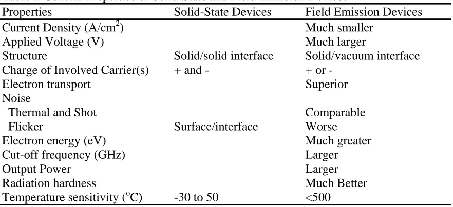
Comparing the characteristics of Solid State and Vacuum Microelectronic devices, as shown in Table I, it is noticed that vacuum is a superior transport medium compared to solids, however space charge limitations on the maximum achievable current density and the fact that only one type of charge carrier is active limit VME applications. Electron beam devices that exploit the vacuum transport environment are the primary application for Field Emission devices. Electron beam devices have been used for application such as flat panel displays, electron microscopy, probe microscopies, microwave tube devices, e-beam lithography, pressure sensors, and space propulsion.
1.8.Fabrication of Field Emitters
Fabrication Of Field Emitters 11
by etching single refractory metal wires, such as Mo and W, for use in electron microscopies. Later in the 1950s arrays of these etched needles were mechanically constructed for use in applications, such as microwave devices. Micro fabrication techniques from the electronics industry was used in the 1960s to develop arrays of gated and un-gated metal tips grown on a single substrate, which became the conventional fabrication method for electronic devices, such as flat panel displays and microwave tubes. In the 1970s arrays of gated and un-gated silicon needles were fabricated. Various coatings or thin films were applied to these field emitter cathodes to improve field emitter performance. To improve reliability of the cathodes current limiting structures, such as ballast resistors and MOSFETs, were incorporated into the fabrication process, substantially increasing the cost to fabricate the cathodes. As shown in Table II the fabrication cost and complexity of these designs increased over time. Beginning in the 1990s newer lower cost processes for field emitter cathodes were developed involving the deposition from solution of materials, for example of CNTs, CNFs and DNPs, and the design of new device structures.
1.9.Summary
Introduction 12
morphology on the field emission characteristics of low-dimensional materials used in efficient fabrication techniques for field emitter cathodes.
1.10.References
1
V.V. Zhirnov, W.B. Choi, J.J. Cuomo, J.J. Hren, Applied Surface Science, 94-5, 123, (1996).
2
V.V. Zhirnov, E.I. Givargizov, P.S. Plekhanov, Journal Of Vacuum Science & Technology B, 13, 418, (1995).
3
D. Temple, W.D. Palmer, L.N. Yadon, J.E. Mancusi, D. Vellenga, G.E. Mcguire, Journal Of Vacuum Science & Technology A, 16, 1980, (1998).
4
V.P. Mammana, D. Jaeger, O. Shenderova, G.E. Mcguire, Journal Of Vacuum Science & Technology A, 22, 1455, (2004).
5
R.G. Forbes, Solid-State Electronics, 45, 779, (2001).
6
W.B. Choi, Y.W. Jin, H.Y. Kim, S.J. Lee, M.J. Yun, J.H. Kang, Y.S. Choi, N.S. Park, N.S. Lee, J.M. Kim, Applied Physics Letters, 78, 1547, (2001).
7
W.B. Choi, J.J. Cuomo, V.V. Zhirnov, A.F. Myers, J.J. Hren, Applied Physics Letters, 68, 720, (1996).
8
G. Fursey, Field Emission In Vacuum Microelectronics, (Kluwer Academic, New York, 2005).
9
C.B. Duke, Tunneling In Solids, (Academic Press, New York, 1969).
10
R. Ramprasad, L.R.C. Fonseca, P. Von Allmen, Physical Review B, 62, 5216, (2000).
11
R. Lake, S. Datta, Physical Review B, 45, 6670, (1992).
12
References 13
13
A. Modinos, Field, Thermionic, And Secondary Electron Emission Spectroscopy, (Plenum Press, New York, 1984).
14
R.G. Forbes, C.J. Edgcombe, U. Valdre, Ultramicroscopy, 95, 57, (2003).
15
M.S. Chung, B.G. Yoon, P.H. Cutler, N.M. Miskovsky, Journal Of Vacuum Science & Technology B, 22, 1240, 2004.
16
R. Gomer, Field Emission and Field Ionization, (American Institute of Physics, New York, 1993).
17
V.V. Zhirnov, L. Bormatova, E.I. Givargizov, P.S. Plekanov, U.T. Son, A.V. Galdetsky, B.A. Belyavsky, Applied Surface Science, 94/95, 144 (1995).
18
R.N. Thomas, R.A. Wickstro, D.K. Schroder, H.C. Nathanson, , Solid-State Electronics, 17, 155 (1974).
19
D. Temple, Materials Science And Engineering, R24, 185, (1999).
20
Y.S. Choi, J.H. Kang, H.Y. Kim, et. al., Applied Surface Science 221, 370 (2004).
21
D. Kang, V.V. Zhirnov, R.C. Sanwald, et al., Journal Of Vacuum Science & Technology B, 19, 50 (2001).
22
W.B. Choi, J.J. Cuomo, V.V. Zhirnov, et al, Appl. Phys. Lett., 68, 29 (1996).
23
Intel, :http://intel.com/education/makingchips/multiple.htm.
Introduction 14
Table I. General Properties of Solid-State and Field Emission Devices
Properties Solid-State Devices Field Emission Devices
Current Density (A/cm2) Much smaller
Applied Voltage (V) Much larger
Structure Solid/solid interface Solid/vacuum interface
Charge of Involved Carrier(s) + and - + or -
Electron transport Superior
Noise
Thermal and Shot Comparable
Flicker Surface/interface Worse
Electron energy (eV) Much greater
Cut-off frequency (GHz) Larger
Output Power Larger
Radiation hardness Much Better
15
Table II. Processes used for fabrication of specific emitter structures, including the approximate number of masks, total fabrication steps and amount of energy and material required.
Type Tip Process # Masks # Steps Energy Budget Ref
Needle Etched 0 3 Low 16
Tip array Etched 0 5 Low 17
Tip Array Etched 1 10 Medium 18
Gated Tip Grown 2 50 High 19
Gated Tip Etched 6 80 High 19
Coated Gated Tip Grown 6 90 High 19
Back-Gate Grown 2 20 High 20
Coated Needle Grown 0 8 Medium 21
Coated Needle Deposited 0 6 Low 22
Back-Gate Deposited 1 15 Medium 4
Introduction 16
17
18
Chapter 2.
Local electrostatic effects of surface structure on field emission:
Metal on metal composite cathodes
by
D. L. Jaeger and J. J. Hren
Department of Materials Science and Engineering, North Carolina State University, Raleigh, NC 27695-7907
and V. V. Zhirnov
Semiconductor Research Corporation, Research Triangle Park, North Carolina 27709-2053
published in
Abstract 19
2.1.Abstract
We examined the classical electrostatic effects due to geometric surface structures on conductive field emission needles numerically using the finite element method (FiEM) and compared our results to several commonly applied analytic relations. Analysis of the morphology of electrochemically prepared Mo needles by high-resolution transmission electron microscopy (HRTEM) was incorporated in the numerical analysis in the form of small surface protrusions and gross needle shape. We found that the error between the electrostatic potential defined by popular analytic equations and both analytic equations derived in prolate spheroidal coordinates and FiEM results was significant for ellipsoidal needles with and without surface protrusions. The morphology of the surface protrusion was found to introduce a significant nonlinear potential barrier near the needle surface. Finally we numerically analyzed a non-symmetric, non-homogeneous experimental needle indicating that even larger errors in the electrostatic potential can be expected relative to analytic equations.
2.2.Introduction
Local Electrostatic Effects Of Surface Structure On Field Emission 20
structure is a common practice in the experimental field emission community. The magnitude of the electrostatic field at the emitting surface is estimated using idealized geometrical parameters and rough analytical approximations; e.g. F≅V/5r for field emission microscopy (FEM) geometry,6 or F=(h/r)F0 for planar geometry.7 More complicated analytical relations have been derived for idealized structures, such as ellipsoids,8,9 hyperboloids,10 prolate spheroids,11 and for gated10 and ungated12 arrays of emitters. However, these relations suffer from an inability to account for geometrical and material irregularities that perturb the morphology from the simple geometries that these relations were derived to solve.
Introduction 21
Understanding the electrostatic field and its interaction with matter is clearly a fundamental question of great significance to the field emission community. You would expect that after 200+ years of development, that the fundamental questions of how the electrostatic field interacts with metallic needles would be answered. On the contrary, many such questions have been debated by the field emission community over several decades but still not adequately addressed. One such fundamental question is whether observed emission phenomena are due to irreversible changes, e.g. in the shape and morphology of the emitting structure by the formation of nanometer-scale protrusions. Another related and fundamental question is how to define the emission area. Recently, Richard Forbes argued that derivation of the emission area using simple models, such as α r2, is inaccurate for fundamental physical reasons, and gives values much smaller than the physical area from which electrons are emitted,13 The community is therefore will aware of problems caused by electrostatic field effects and efforts underway to develop more accurate models for the analyses of field emission experiments.
Local Electrostatic Effects Of Surface Structure On Field Emission 22
determine field enhancement very near a metal surface and can only be resolved by HRTEM, and thus determine unambiguously whether some “exotic” or unexpected localized event is dominating the emission process.
In this paper the electric field on an emitting surface was numerically calculated based on the exact geometry of the tip as determined from HRTEM analysis. Field enhancement effects due to aspect ratios, curvature, and multistage structures were modeled using the Finite Element Method and compared to the analytical models most often used to analyze experimental data. Four specific areas of experimental interest were considered in this work: (1) Idealized Single Tip Field Enhancement Effects, (2) Array Tip Density Electrostatic Effects, (3) Multistage Field Enhancement Effects, and (4) Field Enhancement Effects at experimental tips with inhomogeneous geometry.
2.3.Simulation and Method
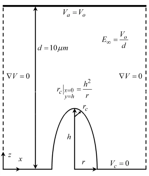
Simulation Method 23
The two dimensional Laplace’s equation in Cartesian coordinates for a source charge free homogeneous medium,
2 2
2
2 2
( , ) ( , )
( , ) V x y V x y 0
V x y
x y
∂ ∂
∇ = + =
∂ ∂ (1)
was used to analyze the field distributions for asymmetrical morphologies and arrays of tips, using the corresponding Dirichlet boundary conditions for constant voltage surfaces,
( )
appliedV rK =V , and the Neumann boundary conditions for symmetry axes, ∇V r
( )
K =0, as illustrated in Figure 1. Single tip field enhancement was analyzed in three dimensions using a cylindrical transformation of the two dimensional numerical domain into the three dimensional physical domain of the idealized diode structure. The size of the physical domain was chosen such that effects of electrostatic shielding did not significantly affect the results. Assuming the problem has azimuthal symmetry, Laplace’s equation in cylindrical coordinates reduces to:( )
2( )
2
2
, ,
1
( , ) V r z V r z 0
V r z r
r r r z
∂ ∂
⎛ ⎞
∂
∇ = ⎜ ⎟+ =
∂ ⎝ ∂ ⎠ ∂ (2)
This allowed a significant reduction in the computational resources required for a three dimensional solution of Laplace’s equation on the problem domain. The three dimensional formulation of Laplace’s equation also provided a higher order of accuracy in modeling the actual fields experienced by tunneling electrons near a metallic surface. The morphology of the needles modeled was necessarily limited to rotationally symmetric structures and needle density effects in arrays were not modeled.
The finite element method (FiEM) was used to solve the resulting Laplace equation,
( )
2
0 V r
∇ K = , using the Galerkin weak formulation of the elliptic partial differential equation.
Local Electrostatic Effects Of Surface Structure On Field Emission 24
numerical. The computational mesh was adaptively refined in regions where heterogeneities and/or high electrostatic fields existed, providing very dense meshes in these regions which capture the character of the rapid field changes near the surface that are of interest in field emission studies. A significant decrease in the computational cost of solving for the potential and fields, while a high level of accuracy was possible in regions of interest, was achieved in this manner. Laplace’s equation was solved for the potential within the numerical domain at the nodes of the generated meshes, with the resulting field strength found by solving Gauss’s law, E
( )
rK =−∇V( )
rK . Linear triangular shape functions were used to construct the linear system of equations that defines the solution in the numerical domain. Dirichlet boundary conditions defined the voltages applied to the anode and cathode surfaces, while Neumann boundary conditions defined the symmetry planes of the numerical domain. The Matlab PDE toolbox14 was used to construct the adaptively refined computational grid and solve the resulting system of linear equations for the Laplace equation over the domain using the Finite Element Method.2.4.Results and Discussion
2.4.1.Idealized Single Tip Field Enhancement Effects
Results And Discussion 25
needle centroid of a half ellipsoid of revolution on a plane cathode separated from a plane anode was derived by several authors as8,9,15:
( )
2 2 2 2
2 2
2 2 2 2
2 2
ln 2
1
ln 2
z h r h r
z
z h r
V z E z
h h r h r
h
h h r
∞ ⎛ ⎛ + − ⎞ − ⎞ ⎜ ⎜⎜ ⎟⎟− ⎟ ⎜ ⎝ − − ⎠ ⎟ = ⎜ − ⎟ ⎛ + − ⎞ − ⎜ ⎜ ⎟− ⎟ ⎜ ⎜ ⎟ ⎟ ⎜ ⎝ − − ⎠ ⎟ ⎝ ⎠ (3a)
Using Gauss’s law the field at the ellipsoid apex at an applied anode bias V0 and anode
cathode plate separation d is:
0 0 3d V E d γ
= (3b)
where the three dimensional field enhancement factor γ3d and the radius of curvature at the ellipsoid surface along the centroid, rc, are:
(
)
3 2 2 23
2 2 2 2
2
2 2
2 2
ln 4 2
ln 2
c d
c h
h r r
h
h h r h r
hr
r h
h h r
γ = − ≅ ⎡ ⎛ + − ⎞ − ⎤ ⎛ ⎞− ⎜ ⎟ − ⎢ ⎜⎜ ⎟⎟ ⎥ ⎝ ⎠ ⎢ ⎝ − − ⎠ ⎥ ⎣ ⎦ (3c) 2 0 x c y h r r h =
= = (3d)
The correspondence in field magnification factors between the three dimensional ellipsoidal cylinder and two dimensional ellipsoidal wedge is:
3 2 2 ln 4 c d d c h r h r γ γ = ⎛ ⎞ ⎜ ⎟ ⎝ ⎠ (3e)
Local Electrostatic Effects Of Surface Structure On Field Emission 26
( )
(
c2)
1c c r V z E z
r r z
γ
∞
⎛ ⋅ ⎞
= ⎜⎜ + ⎟⎟
+
⎝ ⎠ (4a)
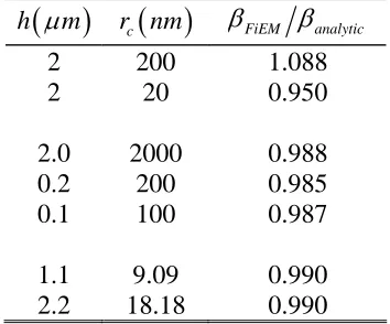
The numerical approach converged to the analytical results rapidly using adaptively refined meshes in the calculations. The FEM results for coarse meshes that do not reflect the structure of the emitter geometry corresponded well to the analytical results in the intermediate regime between the cathode and anode; however, close to regions of high curvature, where emission is assumed to occur, the numerical results diverged significantly from the analytical results. To overcome this weakness the computational grid was adaptively corrected, resulting in a satisfactory convergence between the analytical and numeric results, as illustrated in Table I . The distance between nodes in the computational mesh near the region of emission was approximately 0.1 nm, an assumed atomic lower limit to the smoothness of the material surface, that gave a satisfactory divergence between the numerical and analytical approaches.
Comparing the numerical and analytical results with a common experimental relation for the field enhancement, as shown in Figure 3 for high aspect ratio structures with small radii of curvature, the experimental relation can overstate the field enhancement effect of the structures geometry by an order of magnitude or more for a simple idealized ellipsoidal structure. The potential in the direction normal to the tip apex surface was calculated using two analytic expressions due to Galdetskiy, Eq. (3a), and Zhirnov, Eq. (4a), respectively and interpolated from the FiEM solution, as shown in
Results And Discussion 27
order to correct for this lack of agreement far from the needle apex, Eq. (4a) was modified into the form:
( )
(
)
(
c2(
)(
)
)
oc c
r z d
V z E z h E
z r r d
∞
−
= + +
+ + (4b)
however this modified functional also does not approximate the FiEM results accurately near the needle apex. This discrepancy near the needle apex between Galdetskiy’s rigorously derived potential relation, Eq. (3a), Zhirnov’s physically based relation, Eq. (4a), and the modified formula, Eq. (4b), is a result of the physically non ideal structure of the numerical mesh, which is reminiscent of the actual atomic structure of the needle surface, where local atomic scale features perturb the surface geometry from the ideal shapes considered in Galdetskiy’s analysis.
The observed divergence between the numerical and analytical results near the metal surface is understandable when examined with respect to the nature of the material surface used in the two approaches. The analytical approach assumes the ellipsoidal metal surface is a continuously smooth surface without any atomic scale features, while the mesh used in the numerical approach is a discretely smooth surface that could be used to represent atomic surface features. The nature of the numerical approach may therefore qualitatively model the electrostatic field disturbances due to the surface atomic lattice, which for features approaching atomic dimension, may not be adequately described as a mathematically smooth surface.
2.4.2.Multistage Field Enhancement Effects
Local Electrostatic Effects Of Surface Structure On Field Emission 28
degree of field enhancement.19-22 Using the preceding information and conditions, we simulated the effects of multiple ellipsoidal asperities present on an ellipsoidal tip. Field enhancement factors for two component structures have been presented as the two step field enhancement approach (TSFE),23 where
(
)
2 1 1 1 0 0
E =γ E =γ γ E (5)
If we consider structures consisting of N distinct stages or substructures, which we will refer to as the multistage field enhancement effect, MSFE, the field enhancement factor for these structures has been given as24:
0 0 N
i i
E γ E
=
=
∏
(6)The geometric model of this composite stage needle structure consisted of individual ellipsoids layered on top of each other, largest to smallest, with the centroid of a small ellipse being aligned with apex of a large ellipse. This resulted in angles approaching 0o at the intersection between the two ellipses as Dsmall → Dlarge and approaching 90o as Dsmall << Dlarge, where DR is the dimensionality of the structure.
Results And Discussion 29
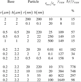
distribution across the apexes of the asperities were continuous and differentiable along with exhibiting the previously described local maximums in field intensity, indicating that field affected deposition processes, such as dielectrophoresis, that are strongly influenced by the magnitude and/or gradient of the localized surface electric field, will preferentially occur in those regions where the magnitude of the field strength or gradient is greatest. The field intensity roughly varies with the geometrical variations between the base tip and the asperities at these locations; however, strong discrepancies arise near the interface regions between the structures.
The agreement between analytic and numeric results for the field enhancement at the site of maximum emission for a two layer geometric system is presented in Figure 6 and Table II. The variation in field intensity about the centroids of these surface structures could increase the maximum fields by an order of magnitude, producing highly localized field enhancement effects around these structures. The geometric agreement between the base structure and asperity has a demonstrative effect on the agreement between the analytic and numerical results. Assuming the geometric mismatch can be quantified as some parameter
α, α~1 for very significant geometric mismatches and α<<1 for slight geometric mismatches. Multiple asperities layered on top of one another showed a similar trend of increasing the maximum fields induced at the emitter surface, while the relative geometric match between each successive asperity layer on the surface of the emitter affected the magnitude of such enhancement as:
0 1
N
i i i
E α γ E
=
⎛ ⎞
= ⎜ ⎟
⎝
∏
⎠ (7)where αi is the degree of geometric mismatch between the asperity and it’s base, the ideal
Local Electrostatic Effects Of Surface Structure On Field Emission 30
effects produced maximum fields much less than the ideal N-stage field enhancement mechanism predicts, such that some αis < 1. Simulations show that multiplicative scaling of
field enhancement effects of multiple structures mounted on one another does not generally occur for the typical needle structures used in field emission. The effects for a structure of multiple spheres, in which the radii of each sphere is one-half the radii of the previous sphere in which the smaller sphere is embedded, are presented in Figure 7. Assuming that the degree of geometric mismatch is equivalent between each stage, then the MSFE can be expressed as:
(
1)
0 N NE = α γ− E (8)
indicating that the disagreement between the ideal MSFE model and the numeric will scale as the Nth power. This behavior is indeed observed in the lack of agreement between the MSFE results and FiEM results, where FiEM 0.53
ideal MSFE
α
α , indicating that the ideal MSFE
model can significantly overstate multistage field effects.
Examination of the potential barrier, which includes Jensen’s “analytic” image charge potential,26 for a small embedded particle on the surface of a relatively large elliptical substrate, Figure 8, shows that the large field enhancement is effective only within a relatively small distance near the surface and the potential is highly nonlinear. Simple approximations using a “standard” image charge affected triangular potential barrier may not prove accurate due to this nonlinear potential barrier, which rapidly diverges from the ideal triangular image affected barrier within 5 Å of the metal surface.
Results And Discussion 31
numeric results, with the best agreement being a base sphere with ellipsoid and spherical asperities. However the maximum field enhancement observed resulted from small, high aspect ratio ellipsoidal asperities on large, high aspect ratio ellipsoidal base tips, where the
αis ≈ 1. Use of a fractal/dendritic surface therefore may not provide nearly as much benefit,
as the MSFE model would indicate. The stability of these types of surfaces would also be of concern due to thermal/field-enhanced diffusion and resistive heating of the dendrites, resulting in thermal diffusion or explosive destruction of the dendrites.
2.4.3.Geometrically Inhomogeneous Needle Field Enhancement Effects
Local Electrostatic Effects Of Surface Structure On Field Emission 32
ellipsoidal needle with a radius of curvature determined by the conventional algebraic method.
A “precise” resolution of the 3D fields of irregularly shaped needles requires several micrographs of the needle at different tilt angles to account for the surface inhomogeneities that exist and a true 3D finite element mesh that will not suffer the problems associated with the coordinate transformations. 2D slab solutions of these needles provide qualitative potential/field distribution information, however they do not account for dimensional effects that can have unknown effects.
2.5.Conclusions
Conclusions 33
revealing that local surface structure significantly affects local electrostatic fields, shifting the magnitude and distribution of the fields, and therefore the physical processes influenced by these fields may be significantly altered in scope and intensity by this effect. These nano and mesoscale electrostatic perturbations, which are a function only of geometric parameters of the composite metal structure, are complex phenomena that are extremely difficult to analyze except with the use of sophisticated numerical methods that account for the multiscale nature of these structures. Understanding and quantifying these multiscale effects thus requires nanoscale resolution of the morphology, such as modern high-resolution electron microscopy provides, in concert with sophisticated numerical procedures.
2.6.References
1
J. Itoh, Y. Tohma, K. Morikawa, S. Kanemaru, and K. Shimizu, J. Vac. Sci. Technol. B, 13, 1968, (1995).
2
G. Mesa, E. Dobado-Fuentes, and J.J. Saenz, J. Appl. Phys., 79, 39, (1996).
3
R.L. Hartman, W.A. Mackie, and P.R. Davis, J. Vac. Sci. Technol. B, 12, 754, (1994).
4
W.B. Herrmannsfeldt, I. Becker, I. Brodie, A. Rosengreen, and C.A. Spindt, Nucl. Instrum. Methods Phys. Res. A, 298, 39, (1990).
5
L.R.C. Fonseca, Paul von Allmen, and R. Ramprasad, J. Appl. Phys., 87, 2253, (2000).
6
R. Gomer, Field Emission and Field Ionization, (Harvard Univ. Press, Cambridge, MA, 1961).
7
T. Utsumi, IEEE Trans. Elect. Dev., 38, 2276, (1991).
8
H. G. Kosmahl, IEEE Trans. Elect. Dev., 38, 1534, (1991).
9
Local Electrostatic Effects Of Surface Structure On Field Emission 34
10
K.L. Jensen, E.G. Zaidman, M.A. Kodis, C. Hor, P. Mukhopadhyay-Phillips, K. Nguyen and L. Malsawma, Appl. Surf. Sci., 111, 204, (1997).
11
L.H. Pan, T.E. Sullivan, V.J. Peridier, P.H. Cutler, and N.M. Miskovsky, Appl. Phys. Lett., 65, 2151, (1994).
12
J.D. Levine, RCA Review, 32, 144, (1971).
13
R.G. Forbes, Solid State Elect., 45, 779, (2001).
14
Partial Differential Equation Toolbox Users Guide, The MathWorks, (1996). available at http://www.mathworks.com/access/helpdesk/help/toolbox/pde/pde.shtml
15
D.A. Kirkpatrick, A. Mankofsky, and K.T. Tsang, Appl. Phys. Lett., 60, 2065, (1992).
16
J. D. Nordgard, J. Appl. Phys., 48, 3042, (1977).
17
V.V. Zhirnov, J. Phys. IV, 6(C5), 107, (1996).
18
C.J. Edgcombe and U. Valdre, J. Microscopy, 203, 188, (2001).
19
D. Atlan, G. Gardet, V.T. Binh., N. Garcia, and J. J. Saenz, Ultramicroscopy, 42, 154, (1992).
20
V.T. Binh, S.T. Purcell, V. Semet, and F. Feschet, Appl. Surf. Sci., 130-132, 803, (1998).
21
O.B. Isayeva, M.V. Eliseev, A.G. Rozhnev, and N.M. Ryskin, Solid State Elect., 45, 871, (2001).
22
D.Y. Zhong, G.Y. Zhang, S. Liu, T. Sakurai, and E.G. Wang, Appl. Phys. Lett., 80, 506, (2002).
23
V.V Zhirnov, E.I. Givargizov, and P.S. Plekhanov, J. Vac. Sci. and Techn. B, 13, 418, (1995).
24
References 35
25
N.M. Ryskin, A.G. Rozhnev, and D.I. Trubetskov, Technical Digest of IVMC’97, Kyongju, Korea, 310, (1997).
26
K.L. Jensen, J. Appl. Phys., 88, 4455, (2000).
Local Electrostatic Effects Of Surface Structure On Field Emission 36
Table I Degree of agreement between analytical and numerical approaches for various model geometries.
( )
h μm r nmc
( )
βFiEM βanalytic2 200 1.088
2 20 0.950
2.0 2000 0.988
0.2 200 0.985
0.1 100 0.987
37
Table II. Percent error between analytic models and numerical results for the maximum field enhancement achievable at the composite needle surface.
Base Particle
base tip
r r γFiEM Δγ γFiEM
( )
r μm h
( )
μm r nm( )
h nm( )
%2 2 200 200 10 8 15
2 2 0.1 0.1 20 8 11
0.5 0.5 20 220 25 109 57
0.5 0.5 2 22 250 149 15
1 1 2 22 500 149 15
0.2 2.2 20 20 0.01 61 182
0.2 2.2 2 2 0.1 127 34
0.2 2.2 0.5 0.5 0.4 158 9
0.2 2.2 20 220 10 371 778
0.2 2.2 10 110 20 384 748
0.2 2.2 5 55 40 822 297
Local Electrostatic Effects Of Surface Structure On Field Emission 38
39
Local Electrostatic Effects Of Surface Structure On Field Emission 40
41
Local Electrostatic Effects Of Surface Structure On Field Emission 42
43
Local Electrostatic Effects Of Surface Structure On Field Emission 44
45
Local Electrostatic Effects Of Surface Structure On Field Emission 46
47
48
Chapter 3.
Electrostatic effects of conformal and isolated diamond
nanodots on field emission
by
D. L. Jaeger and J. J. Hren
Department of Materials Science and Engineering, North Carolina State University, Raleigh, NC 27695-7907
and V. V. Zhirnov
Department of Materials Science and Engineering, North Carolina State University, Raleigh, NC 27695-7907 and
Semiconductor Research Corporation, Research Triangle Park, North Carolina 27709-2053
Abstract 49
3.1.Abstract
Extraction and analysis of reliable data from field emission measurements of needle structures with diamond coatings is a vexing and complex problem, but of great importance in understanding the electron emission mechanism. The electrostatic fields of diamond/metal composite needle structures were numerically analyzed based on experimental input describing their exact geometry and chemical composition. We demonstrate in this article an expectation that electrostatically influenced emission and particle transport properties differentiate bare metal needle substrates, metal needles with nonconductive coatings of isolated particles, and metal needles with continuous coatings of nonconductive films. This behavior partially explanations the existence of “anomalous” and “normal” thickness effects experienced by systems of diamond coatings.
3.2.Introduction
Composite field emitters consisting of a conductive needle substrate with coatings of wide band gap materials (e.g. diamond, AlN, etc.) have been studied extensively over the past few years1,2,3,4. It was found experimentally that such coatings offer improvements of emission properties over their metallic needle-shaped emitter substrates. However, the mechanism of electron emission in such structures is not completely understood, because they are complex. The existence of surface charge, new interfaces, material inhomogeneities, and/or doping can have dramatic effects on the emission behavior of these composite emitters.
Electrostatic effects of conformal and isolated diamond nanodots … 50
Experimentally the emission voltage of emitters coated with diamond5 and AlN6,7 films, with a thickness greater than 20-50 nm, was observed to decrease (relative to the film thickness, as the film thickness decreased). These observations are sometimes referred to as the “normal” thickness effect. Such behavior has typically been associated with the resistive voltage drop across the films or to negative space charge within the insulating coating. One might project that this trend would continue with even thinner diamond coatings, the ultimate limit being a single, isolated particle that would exhibit optimum emission properties. Later studies with much thinner diamond and AlN deposits on metal needles indicated that the emission voltage was substantially increased, contradicting the previous predictions of the “normal” thickness effect6,7 , therefore we refer to this latter behavior as the “anomalous” thickness effect8. This thickness dependent emission behavior exhibited emission properties that were at an optimum for relatively thin continuous films, where the “anomalous” thickness effects are assumed to appreciably influence the emission process.
Models of the emission mechanisms of such structures involve assumptions that significantly affect their valid analysis. We have striven to reduce such assumptions to a minimum, so that we can derive a quantitative model for their field emission behavior. Theoretical efforts should be based on solid experimental input therefore the results presented in this work were obtained for an actual composite diamond-metal tip system characterized by high resolution transmission electron microscopy before and after field emission measurements9.
Introduction 51
microscopy (HRTEM) and electron energy loss spectroscopy (EELS), before and after emission, the exact geometry and chemical composition of the composite cathodes was determined. We previously used a similar approach in the electrostatic analysis of metal needles exhibiting geometric perturbations from ideal shapes, showing that analytic methods are often not accurate and lead to erroneous analyses10. The local electric potentials and fields at the emitting surfaces were numerically calculated using morphological and compositional physical information derived from this data.
3.3.Experimental Input
Field emission experiments carried out on metal- nanodiamond coated needles exhibit a thickness dependent shift of the threshold voltage and current evolution with applied bias9. The field emission characteristics generally improve as the film thickness decreases: however, we have consistently observed an “anomalous” thickness dependence for very thin coatings, including one consisting of a single isolated nanodiamond particle (d≈5 nm)9. For such nanometer dimension coatings, emission characteristics are degraded, by comparison with the emission observed from the same bare metallic needle. Such anomalous thickness dependent field emission behavior is not confined to nanodiamond coatings, it has been also observed in metal field emitters with AlN coatings1,2. Such counter-intuitive behavior suggests that some size-selective mechanisms take place at or below a critical coating thickness.
Electrostatic effects of conformal and isolated diamond nanodots … 52
1) HRTEM of typical as prepared needles indicates strong deviations from ideal geometric structures.
2) No traces of a graphite phase were found in any nanodiamond clusters before field emission using HRTEM and EELS analysis9.
3) HRTEM did not reveal any measurable changes in the metal substrate geometry that could account for the observed changes in emission after both nanodiamond deposition and field emission.
From HRTEM of a Mo needle with a coating of discrete isolated nanodiamond particles, the particles appear to be embedded in the Mo substrate at or near the region of minimum radius of curvature following field emission and are ‘spherical’ in shape with radii of approximately 2.6 nm9.
3.4.Numerical Method
Bulk diamond physical parameters were assumed throughout the numerical analysis of the Mo-diamond nanodot needles. The nanodiamond particles were assumed to be insulating and that surface charge could be neglected. The three dimensional classic electrostatic field of the structures was analyzed using finite element method solutions to Laplace’s equation. Isoparametric linear elements, an unstructured, adaptively refined computational mesh and the axisymmetry of the physical domain was utilized in the finite element analysis as in our previous study of bare metal needles10.