University of Windsor University of Windsor
Scholarship at UWindsor
Scholarship at UWindsor
Electronic Theses and Dissertations Theses, Dissertations, and Major Papers
1-1-1969
An alpha-numeric character generator for a computer display.
An alpha-numeric character generator for a computer display.
K.G. Sreenivasan
University of Windsor
Follow this and additional works at: https://scholar.uwindsor.ca/etd
Recommended Citation Recommended Citation
Sreenivasan, K.G., "An alpha-numeric character generator for a computer display." (1969). Electronic Theses and Dissertations. 6591.
https://scholar.uwindsor.ca/etd/6591
This online database contains the full-text of PhD dissertations and Masters’ theses of University of Windsor students from 1954 forward. These documents are made available for personal study and research purposes only, in accordance with the Canadian Copyright Act and the Creative Commons license—CC BY-NC-ND (Attribution, Non-Commercial, No Derivative Works). Under this license, works must always be attributed to the copyright holder (original author), cannot be used for any commercial purposes, and may not be altered. Any other use would require the permission of the copyright holder. Students may inquire about withdrawing their dissertation and/or thesis from this database. For additional inquiries, please contact the repository administrator via email
FOR A COMPUTER DISPLAY
by
K.G.SHEENIVASAN
A Thesis
Submitted to the Faculty of Graduate Studies through the Department of Electrical Engineering .in Partial Fulfillment
of the Requirements for the Degree of Master of Applied Science at the
University of Windsor
Windsor, Ontario
1969
UMI N um ber: E C 5 2 7 7 4
INFORMATION TO USERS
The quality of this reproduction is dependent upon the quality of the copy
submitted. Broken or indistinct print, colored or poor quality illustrations and
photographs, print bleed-through, substandard margins, and im proper
alignm ent can adversely affect reproduction.
In the unlikely event that the author did not send a com plete m anuscript
and there are missing pages, these will be noted. Also, if unauthorized
copyright material had to be removed, a note will indicate the deletion.
®
UMI
UMI M icroform EC52774
Copyright 2008 by ProQuest LLC.
All rights reserved. This m icroform edition is protected against
unauthorized copying under Title 17, United States Code.
ProQuest LLC 789 E. Eisenhower Parkway
PO Box 1346 Ann Arbor, Ml 48106-1346
t
(D-CJ
ABSTRACT
Thin thesis describes the logical design and im
plementation of an economical cathode ray tube alpha-numeric
display unit for a Digital Equipment Corporation PDP-8/S
digital computer.
The above device is capable of displaying a part
of the stored data in the computer memory on a cathode ray
tube screen at the rate of approximately 200 characters
per second with good legibility and flicker-free. This rate
could be increased depending upon the writing speed of the
oscilloscope used.
Each displayed character is formed by a series of
dots selected from a
5 x 7
matrix of dots. These dots arein turn generated on the cathode ray'tube screen by a set
of unblanking pulses, fed to the Z-axis of the cathode ray
tube in synchronism with the blanked beam movement.
A storage oscilloscope is used to overcome the
flicker problem obviating the use of a delay line memory
or a core memory. This greatly reduces the cost of the who
le unit. Any conventional storage oscilloscope having a saw
tooth output can be used for the purpose.
constructed for providing flexibility in positioning the ch
aracter on the screen and also control over the start,stop
operation of the device.
The main advantage of this device lies in its si
mplicity in logical design. It also affords the flexibility
for changing the shape of the character by a suitable addi
tion and/or deletion of any of the pulses that go to make
up the character.
. iv
ACKNOWLEDGEMENTS
The author wishes to express his appreciation to
Dr. P.A.V.Thomas for suggesting this project and for his
able guidance throughout its completion. Acknowledgement
must also go to the National Research Council of Canada
for the financial aid which made this project possible.
• v
Page A B S T R A C T ...H i
ACKNOWLEDGEMENTS . . . ... . v
TABLE OF CONTENTS... vi
LIST OF ILLUSTRATIONS... ' . '... viii
Chapter I. INTRODUCTION 1.1. Need for a c.r.t. display unit....,.... 1
1.2. Methods used for generating characters on a c.r.t... 2
1. Scanning... 2
2. Stroke or Waveform... ^ 3. Beam Shaping... k 4. Dot Pattern... 5
1.3. Proposed Method... 6
1 , k . Flicker Problem... 6
II. PDP-8/S 2.1. General Description... 7
2.2. Interfacing Facilities... 7
2.3. Programmed Data Transfers... 9
2 . k , Timing and IOP Generator ... 13
III. CHARACTER GENERATOR AND CONTROL UNIT 3.1. Raster Generation... ... 15
vi
Page
3.2. Description of Character Generator 20
1. Device Selector... 20
2. Buffer Register... 22
3* Counter... 2$
4. Counter Decoder... 25
5* Gating Circuitry for the Generation of Pulse Train... 27
6. Character Decoder... 29
3.3. Operation of the Character Generator... 31
IV. IMPLEMENTATION ... 33
V. CONCLUSIONS ... 37
APPENDIX I - Octal Codes used for the'Character Representation. ... 39
APPENDIX II - Proposed Pattern for the Characters and the Pulse Numbers... 40
APPENDIX III - Flowchart and the Program Listing for Character Generation... 45
APPENDIX IV - Logic N o t a t i o n ... 47
REFERENCES ... 49
VITA AUCTORIS ... 51
vii
Figure Page
1. Methods of character generation... 3
2. Typical IOT Instruction decoding... 8
3. PDP-8/S Instruction timing... 8
k , PDP-8/S Programmed data transfer Interface, n 5. IOP Generator logic... 12
6 . Technique of character generation. ... 16
7 . Block diagram of the proposed character generator unit... 18
8 . Device selector logic... 19
9. Buffer register.,... 21
10. 6-Bit "binary counter... 23
11. Counter decoder... 2^
.12. Pulse selection ’OR* gates... 26
13. Character decoder ... 28
14. Use of IOS to test the Status of External Device ... 30
15. Horizontal deflection time-base circuit.... 34
16 . Proposed patterns for the characters... k0 17. Dot matrix with reference numbers... if. 1 18. The Oscilloscope display... ^7
viii
CHAPTER I
INTRODUCTION
1.1. Need for a cathode ray display unit:
The increasing use of high speed digital computers
has created a demand for high speed read out. This demand
has stimulated the development of methods for generating
alpha-numeric and symbolic information from coded digital
inputs. There are various methods of visualising the digital
information such as printing on paper, displaying on gas
filled indicator tubes or displaying the data on cathode
ray tube (c.r.t.) screen. The principal advantage of dis
playing computer generated information on a c.r.t,screen over
other methods lies in its speed of operation. For' instance
the c.r.t. display units can display up to 2500 characters 1
per second, the limitation being the type of memory buffer
and c.r.t. used and also the operating speed of the computer,
as compared to a teletype which can output only about 10
characters per second. The c.r.t, display units also offer
the possibility of displaying simultaneously a large number
of characters in a small area.
With the addition of light pen device, the c.r.t.
display units offer the possibility of modifying the dis
played data. Yet another feature of the c.r.t. unit is its
1
All the above said featiyres make the c.r.t. disp
lay unit, an attractive output unit for the computer, there
by providing a key solution to the problem of efficient com
munication between the computer and its users.
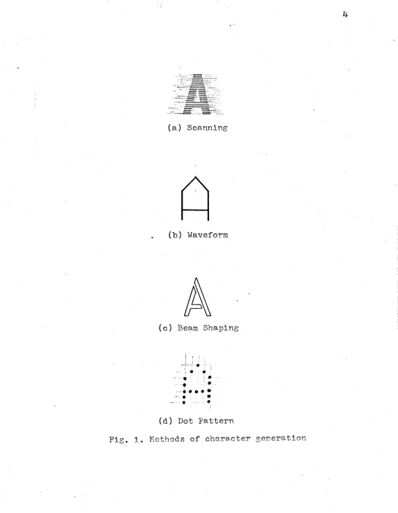
1.2. Methods used for generating characters on a c.r.t. :
The primary requirement of any method used for
character generation is that the generated characters are
legible and distinct. There are various methods available
for the purpose of generating alpha-numeric characters on a
c.r.t. screen satisfying the above requirement. A few of th
em will be described here along with the method chosen for
the display unit constructed for the project under descrip
tion.
2,5 1.2.1. Scanning:
The characters are formed on the c.r.t, screen
in much the same way as the character formation on a tele
vision screen. The character information .stored in the gene
rator, is sequentially sampled in a predetermined order to
obtain intensity signals for modulating the disrlay genera
tor output. The appropriate area of the display must be
scanned in synchronism with the character generator. A small
raster is generated separately by the control pulse generator
3
which synchronizes the raster scan with the scanning of the
character store. Refer to fig.l(a)for a typical character
display generated by the scanning method.
1 1.2.2. Stroke or Waveform:
Each character is formed by a set of ^5 degree
angled strokes in addition to the horizontal and vertical
strokes. The characters are stored in the generator as X
-and Y deflection -and intensity information. This information
is simultaneously sampled to form three parametric analog
waveforms. These are used by the display generator to draw
out the character much as a pencil is used. Refer fig. 1 (b).
Even though this method provides very good legibility for
the displayed characters , it calls for complex circuitry
to produce the strokes of the proper type to draw out the
characters. „
1.2.3. Beam Shaping:
In this method the characters are formed by pass
ing the c.r.t. writing beam through a stencil mask. The
mask contains all the characters to be displayed. The des
ired character is selected for display by a proper choice
of X and Y coordinates of beam deflection. As it can be seen
this method requires a specifically built c.r.t. and it is
not suitable for use with the conventional oscilloscope.
Refer to fig.l(c).
/\
(b) Waveform
(c) Beam Shaping
- • . •
— - • ; •
(d) Dot Pattern
Fig. 1. Methods of character generation i i
1*3.^ 1 .2 .4-. Dot Pattern:
Characters are formed by a set of selected dots
usually from a 5 x 7 matrix of dots. These dots are formed
on the face of the c.r.t. screen either by selection of sui
table X and Y coordinates for each dot using digital to ana
log converters and blanking the beam movement when it changes
position or by a set o f .unblanking pulses generated in sync
hronism with the beam movement which is blanked.
In the present available display units using the
dot pattern with unblanking pulses, the pulse train required
for each character is obtained by a proper selection of rows
and columns of a core matrix memory. This memory usually
consists of 35 magnetic cores in a 5 x 7 array. Each core
contains a set and reset winding. In addition, a read out
winding is threaded .through the matrix to simulate the cha
racter to be displayed. These read out wires will provide
the unique pulse train required for each character when
all the columns are set and the rows are reset sequentially.
Fig.1 (d)gives a typical display generated for a character
using the dot pattern method.
The number of dots or scanning lines contained in
the individual characters of f i g . l ( a ) ,(d) can be increased
to improve the resolution. But such an increase will incre
ase the cost and size of the unit and decrease the writing
speed.
1.3. Proposed, method:
After a careful' review of the various methods des
cribed above it was decided to adopt the dot pattern of cha
racter generation using unblanking pulses with the blanked
beam movement, as it offered good legibility and also sim
plicity in logical design.
To generate the unique pulse train for each chara-■1»3 * ^
cter, the costly magnetic core technique was not used. Ins
tead a relatively cheap clock and gating circuitry were
used for generating the required pulse .train. To display
these dots on the c.r.t. screen at the proper positions, a
small raster was generated on the face of the c.r.t. screen
in synchronism with the pulse train generation.
1 .^. Flicker problem:
Once the characters are generated, they have to
be maintained in such a way that the display is flicker free.
This problem is traditionally overcome by providing a buffer
memory and whole display being repeated such that no percep
tible flicker appears on the c.r.t. But another and less
costlier way of avoiding the flicker problem is to use the
storage oscilloscope for the display. In the project under
description, a storage oscilloscope has been used to econo
mise in the overall design.although this does not provide
the possibility for changing a character or erasing a portion
of the displayed data.
CHAPTER II
PDP-8/S
7 '2.1. General description:
PDP-8/S is a small general purpose computer with
a processor and a random access core memory of ^096 words.
This is a serial, one address, fixed word length of 12 bits
(plus parity) computer and uses 2 ’s complement arithmetic.
Alpha-numeric characters are stored in 8 bit ASCII code
format. Standard features include indirect addressing,faci
lities for instruction skipping and program, interruption as
fttnctions of input/output device conditions.
2.2. Interfacing facilities:
Since the maximum utilization of a computer system
depends largely upon the flexibility and number of periphe
ral devices that can be attached to it, the PDP-8/S has been
designed to interface readily with a broad variety of exter
nal equipment.
High capacity and high speed Input/Outpu.t capabi
lities of the PDP-8/S s.llow it to operate a. variety of peri
pheral devices in addition to the standard teletype, tape_
reader etc. It can also be interfaced with c.r.t. display
units and digital plotters. Interfacing of these devices
to the computer requires no modifications and can be
7
achieved in the field.
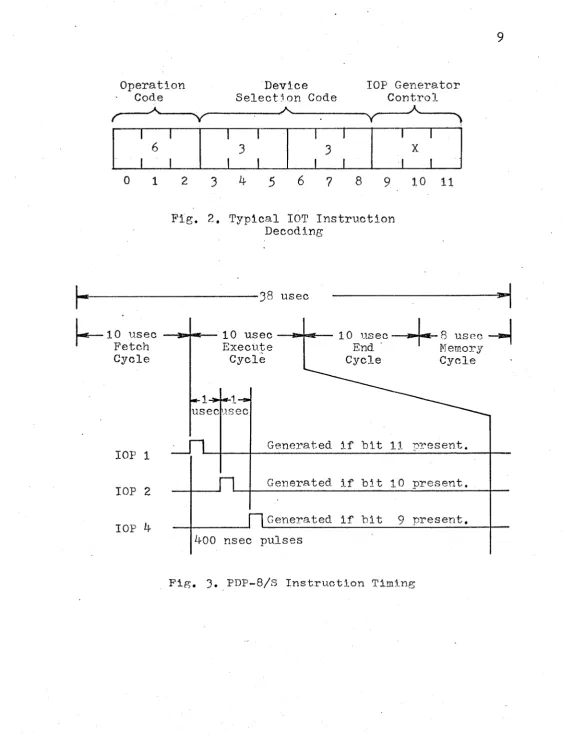
7,10 2.3. Programmed' data transfers:
All the data transfers between the peripheral equ
ipment and the PDP-8/S computer, which are controlled by
programmed instructions in the computer are known as progra
mmed data transfers. This mode of operation utilizes the
basic Input Output Transfer instruction, which is divided
into three parts. Bits 0,1 and 2 contain an operation code
of 6 to specify the Input Output Transfer (I0T) micro inst
ruction, Bits 3 through 8 serve as a device selection code,
which is transmitted to all peripheral equipment and which
activates only the equipment designated by a specific code
number contained within these bits. Bits 9*10 and 11 control
the output of the I0P generator within the processor and
enable or disable the generation of I0P1, I0P2,and I0P^
pulses during each I0T instruction. Figures 2,3 show the
decoding of an I0T instruction and its timing.
A bussed system of Input/Gutput data transfers
imposes the following requirement on the peripheral device.
1. A device selector which samples the select code genera
ted by the IOT instruction and when selected to produce the
IOT command pulses in accordance with the computer generated
input output pu.lses.
9
Operation Device IOP Generator
Code Selection Code Control
f * V --- :---^ ---:--- Y --- A --- >
.. - r ■■ t— 6 I I
T ■ T " ” 3
1 1
1... r "
3
1 1
1 1 ..
X
1 1
0 1 2 3 5 6 ? 8 9 10 11
Pig. 2, Typical IOT Instruction Decoding
38 u s e e --- ^
10 usee Fetch Cycle
10 usee Execute Cycle
10 usee-End Cycle
usee
Generated if hit 1.1. present IOP 1
Generated if bit 10 present IOP 2
Generated if bit 9 present. IOP
if-^-00 nsec pulses
Fig. 3. PDP—8/S Instruction Timing
2. A buffer register to store the information before tran
smitting to or receiving from the accumulator of PDP-8/S.
3. A status flipflop to indicate the ready or busy status
of the peripheral device.
The device selector within each peripheral equip
ment monitors the device selection lines and enables pulse
amplifiers when its assigned select code has been detected
within bits 3 through 8 of an IOT instruction. When enabled
in this manner the pulse amplifiers produce positive or ne
gative IOT pulses when triggered by the associated IOP pul
ses. The IOT pulses in turn perform data transfers to or
from the computer and also control functions within the
peripheral equipment.
In preparation for a normal data transfer, the
computer programme normally checks the ready status of the
receiving device (indicated by a flip flop) by an IOT pulse
and the result is indicated to the input/output skip facil
ity. The input/output skip allows branching of the program
based upon the condition or the availability of peripheral
equipment, effectively making programmed decisions to cont
inue the current program or jump to another subroutine that
services a peripheral device.
The data transfers are carried oitt via the
11
ulator, using upto 12 bits. The program places the contents
of the memory location to be transferred, in the accumulator
and this information is supplied at the bussed connection
for the transfer operation. Fig. ^ shows the information
flow within the computer which effects programmed data tra
nsfers with input/output equipment.
10
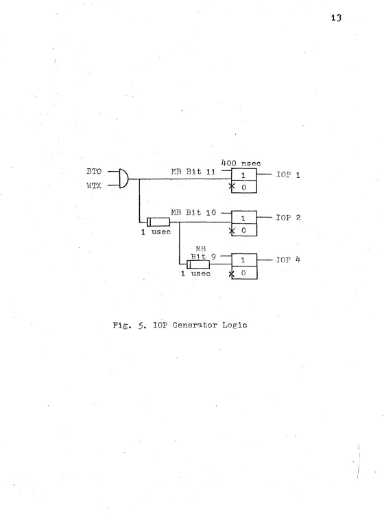
2 , h . , Timing and IOP generator:
When the Instruction Register (IR) decoder detects
an operation code ,6 , it identifies an IOT instruction
and initiates operation of the IOP generator. The logic ■*
diagram, is shown in fig. 5. It consists of three similar
channels, each channel having a gated delay, a gated pulse
amplifier and an output pulse amplifier. Each pulse amplifi
er is provided with a 2 input 'AND' gate. The binary 1 status
of the one of the least signicant bits of the instruction
in the memory buffer supplies the conditioning level of
each of these gates. The other input of the 2 input 'AND1
gates are connected to the output-of a pulse amplifier
through two delay circuits as shoinr in the fig. 5* Thus
depending upon the presence of bits 9.10,and 1 1 , the I0P1,
I0P2 and IOP^i pulses are produced when pulse Inpi.it of the
corresponding 'AND' gate is triggerred.The instruction bit
that enables or disables generation of each IOP pulse,
the corresponding number of the IOT ptilse -produced - in the * Refer to Appendix IV for logic symbols and notation used
Bits 0-2 IOT Instruction Bits 9-11 IOP Pulses Input 12-bit Instruction Word Program Interrupt Request (IR) PROGRAM INTERRUPT FACILITY (PI) CORE MEMORY GENERATOR IOP
I/O SKIP-FACILITY (IOS) ACCUMULATOR REGISTER (AC) MEMORY BUFFER REGISTER
. (MB)
Fig, k . PDP-8/S Programmed Data-Transfer Interface
^00 nsec
BTO
WTX
KB Bit 11 IOP 1
MB Bit 10
IOP 2
1 usee
MB
Bit IOP h
1 usee
Fig. 5. IOP Generator Logic
device selector and event time for each pulse Is
Instruction IOP IOT Event
bit pulse_________ pulse____________ time
11 IOP 1 IOT 1 1
10 IOP 2 IOT 2 2
9 IOP 4 IOT 4 3
CHAPTER III
CHARACTER GENERATOR AND CONTROL UNIT
Before describing the details of the character
generator and its operation, it is appropriate to describe
the technique used,to generate the character,In full and th
required raster generation,
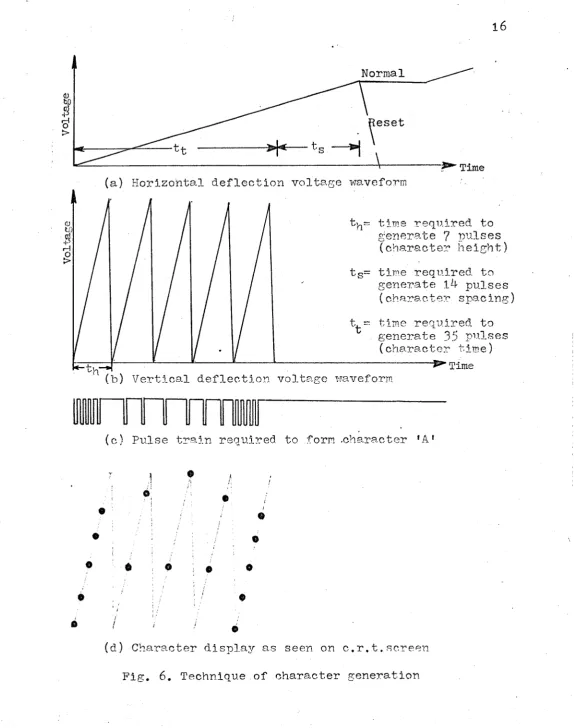
3 ,1 . Raster generation:
A small raster is required to generate the charac
ter display on the c.r.t. screen. The width of this raster
is equal to the height of the character displayed and this
consists of 5 equally spaced near vertical lines. This can
be achieved by applying sawtooth voltage waveforms to both
horizontal and vertical deflection plates of the c.r.t.
simultaneously. The vertical deflection sawtooth voltage
waveform should be made to increase for a duration required
to produce 7 pulses (by the clock) and then be reset. Now
if this vertical deflection waveform is triggered 5 times
at equal intervals namely by pulses 1 ,8 ,1 5 ,22,29 we can
generate the 5 vertical lines required for the formation of
the characters. Refer to f ±g, oft*) . In the present project
this sawtooth waveform was obtained from the oscilloscope.
* Refer to fig. 1?.
15
V
o
l
t
a
g tv,-- time required to
generate 7 pulses (character height)
ts= time requ.ired to generate pulses
(character spacing)
t.= time required to generate 35 pulses
(character time) ^ rpime (b) Vertical deflection voltage waveform
(c) Pulse train required to form .character 'A1
©
©
(d) Character display as seen on c.r.t.screen
Fig. 6 . Technique .of character generation
17
The horizontal deflection votage waveform should
be made to increase for a duration required to produce ^8
pulses, so that it has enough deflection to generate the
character and to provide the spacing for the next to be
generated and then held at the value reached at the end of
^8 pulses. Again when another character is to be generated
this horizontal deflection voltage should be made to increase
from its previous value. It should also have facilities for
resetting to its initial value after generating a certain
number of characters.Fig. 5 (a) shows the shape of the requi
red horizontal deflection waveform. The circuit required to
generate this voltage waveform was designed and constructed
and is described under the chapter "Implementation".
In addition to these deflection voltages, it is
required to generate a unique pulse train for each character
and should be fed to the Z axis of the c.r.t. in synchronism
with the raster generation. If the lines generated by the
above said horizontal and vertical deflections are blanked
and the pulse train is used as unblanking pulses, then the
required display will be formed on the c.r.t, screen. The
method of pulse train generation is described in the follo
wing paragraphs under the present chapter.
A complete diagram is given in fig. 6 showing
the shape of horizontal and vertical deflection waveforms
used, the pulse train required to generate the character 'A'
and the actual display formed on the c.r.t. screen.
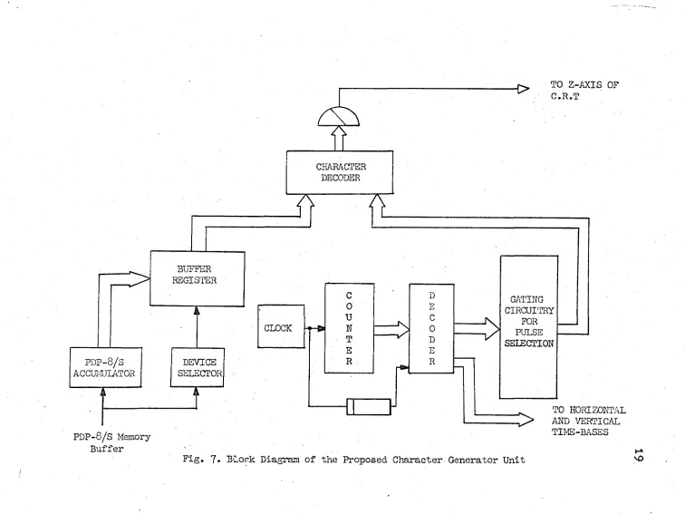
3.2. Description of the character generator
The character generator and control unit consists
of a device selector, a buffer register for temporary storage
of information, a character decoder, a clock, a counter and
counter decoder and the associated gating circuitry for the
generation of pulse trains. A block diagram of the character
generator and the control unit is shown in fig. 7 . The det
ails and working of each of the above mentioned components
are described below.
• 7 3.2.1. Device selector:
The logical representation of the device selector
is shown in fig. 8 . This consists of a 6 input 'NAND1 gate
and three gated pulse amplifiers. These' 6 inputs correspond
to bits 3 through 8 of the memory buffer register ( MB).
Since both negative and positive levels of memory buffer
register bits are available at the bussed connection, any
code between 00 and 77 can be generated by the proper selec
tion of bit levels. For the project under description a code
33 was selected and connections were made accordingly„as
shown in the fig.8 , Thus, this device will be enabled only
when a 33 is present in the IOT instruction.
R e p ro d u c e d w ith p e rm is sio n of the c o p y ri g h t o w n e r. F u rth e r re p ro d u c tio n p ro h ib ite d w it h o u t per m is s io n .
TO Z-AXIS OF
C .R .T
TO HORIZONTAL AND VERTICAL CLOCK DEVICE SELECTOR FDP-8/S ACCUMULATOR CHARACTER DECODER BUFFER REGISTER GATING CIRCUITRY FOR PULSE SELECTION PDP-8/S Memory Buffer TIME-BASES
—vs
-t> +ve
-ve
-t> +ve
■p* -ve
-o +ve
MB Bit 3(0)
MB Bit -i(1 )
MB Bit 3(1)
MB Bit 6(0)
MB Bit 74-t-). MB Bit 8(1)
Fig. 8 . Device Selector Logic
Reproduced with permission of the copyright owner. Further reproduction prohibited without permission. N
A .•
N
D
IOF
kI0P 2
P.A. I0P 1
IOT 1
'TOT 2
21
The level output of this 1NAND* gate is connecte'd
to the level inputs of the three 2 input ‘AND* gates feed
ing the three pulse amplifiers. The trigger inputs of these
gates are connected to the 3 outputs of the IOP pulse gene
rator of the computer. Hence, the three pulse amplifiers
produce the 3 IOT pulses when properly enabled by the devi
ce select code and triggred by the corresponding IOP pulses.
Both negative and positive output pulses are available,
which are used for control purposes.
3.2.2.. Buffer register:
The logical representation of the buffer register
is shown in fig.9. This is a 6 bit flip flop register cap
able of storing a 6 bit information. Even though standard
ASCII code uses an 8 bit code for the alpha-numeric chara
cters, it was found that a 6 bit register is adequate for
our purposes so long as no special character is required
to be stored. Appendix I gives the codes used for each cha
racter. Information is transferred in parallel mode to this
register from the computer via the accumulator -under the
program control of the PDP-8/S, as described earlier under
programmed data transfers. Since this register is capable
of storing only one character at a time, any character is
held only for a time, that is required to display that
par-- ticular character. As the computer can transfer characters
o
i—I
Reproduced with permission of the copyright owner. Further reproduction prohibited without permission.
•F
ig
.
9*
B
u
f
f
e
r
R
e
g
i
s
t
e
23
at a rate much faster than the time required, to generate
them on the screen, it must be kept waiting till the trans
ferred character is generated before another character is
sent into the buffer. This is achieved by a device ready
flip flop as explained later under-'1 Operation1.
3.2.3. Cotmt er:
The counter used for this project is a 6 bit
straight binary counter, whose logic diagram is shown in
f i g . 10* For clarity purposes interconnections between the
flip flops are omitted in the diagram. Since this is a 6
6
bit counter, it is capable of counting upto 2 - 6 k numbers.
The counter is made to reset automatically after counting
upto ^8 through a NAND gate and a pulse amplifier. The fir
st 35 counts are utilized to numbei the 5 x 7 matrix of
pulses and the rest for providing the spacing time between
the characters.
3.2.4. Counter decoder:
A series of 35» 7-input NAND gates, one each for
each of the 35 pulses required to generate the 5 * 7 matrix
of pulses, make up the counter decoder. The logic diagram
of the counter decoder is shown in fig. 11. The six of the
Seven inputs are connected to the level outputs of the cou
nter flip flops as required, and the seventh input is conne
cted to the delayed clock pulse. The clock pulse must be
h
o
o
f
Bit 6 Direct
Clear
Bit 1
Disable clock
Fig.10.. 6-Bit binary Counter
25
Counter bit 1(1)
bit 3(0)
bit M O )
bit 5 (0 )
v \31 s e N umb er 1
bit 6 (0 )
■£5* Pulse Number ,35
Delayed Clock Pulse
Pig. 11, Counter Decoder
249995
delayed before reaching the counter decoder, because the
clock pulses which are used to change the state of the coun
ter cannot be used to sample the counter at the same time,
as. this might result in ambiguity of the pulse number deco
ded. Th(e delay was achieved by means of a single shot multi
vibrator circuit.
Thus each NAND gate is made to decode one pulse.
For example the inputs of the NAND gate which decodes pulse
number 1 are connected to the binary ' O ' outputs of
flip-flops 2,3,^,5,6 and binary '1* output of flip flop 1 of the
counter.
As it can be seen only one NAND gate is enabled
at any one time depending upon the number present in the
counter at that time. The outputs of these NAND gates go
to provide the 35 pulses required for the character gener
ation. They also provide the triggering pulses for the
time-base circuits.
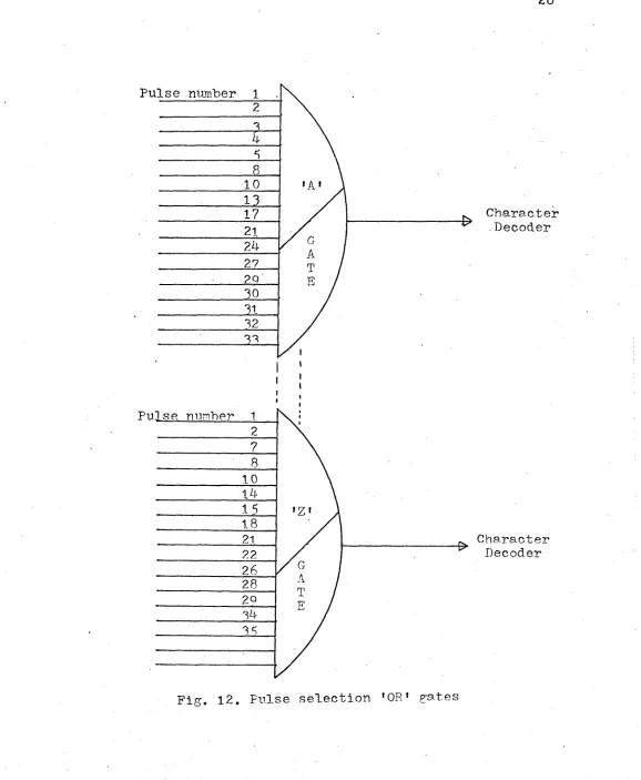
3.2.5. Gating circuitry for the generation of pulse train:
Each character requires a set of pulses depending
upon the its shape of formation. For each character an OR
gate is required whose inputs are equal to the number of
pulses required to form that particular character. The in
puts of these OR gates are fed from the outputs of- the
27
ter decoder as required for each character. The shape of a
character can be changed by changing the input connections
of these OR gates. The pulses required to form each chara
cter and the shapes proposed are shown in Appendix II. As
an example an OR gate with the input pulses required to
form the character "A" is shown in fig. 12.
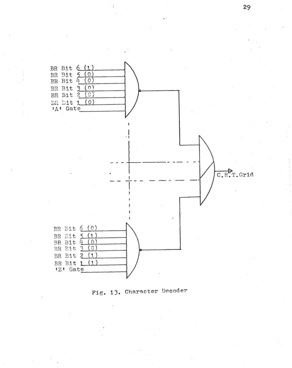
3,2,6. Character decoder:
A series of 7-input NAND gates, one each for sel
ecting each character, make up the character decoder. The
6 of the 7 inputs are fed from the level outputs of the
character generator buffer register flipflops to decode the
character present in the buffer, and the seventh input is
connected from the OR gate which sends the pulse train
reqitired to form the particular character decoded.
Thus it can be seen that when a particular charac
ter is selected,the pulse train to form that character is
is outputted by the character decoder. The logic diagram
and the selection lines required to generate the character
1A * is shown in the fig. 13» For example, to select the
character ‘A* the 6 inputs of one NAND ga.te are connected
to the b i n a r y >0* outputs of b u f f e r r e g i s t e r flipflops 1,2,
3,^,5 and to the binary * 1 * output of flipflop 6 and the
seventh input is connected to character 'A* OR gate.
The outputs of all these decoder NAND gates are
Pulse number 1
24 2? 20
Character .Decoder
Pulse number 1.
10
18
22 26
28
20
Fig. 12. Fuilse selection ’O R ’ g-ates
Character Decoder
29
BR Bit BR Bit BR Bit BR Bit BR Bit
C.R.T.Grid
BR B i
3R Bit
«Z' Gate
Fig. 13. Character Decoder
ORed together and fed to the grid of the c.r.t. to provide .
the intensification or unblanking pulses.
3.3. Operation of the character generator:
The entire operation of the character generator is
program controlled. An I0T^ pulse is generated by the instru
ction 633^ to test whether the device is ready to receive
data. This operation is performed by a 2-input NAND gate in
the device connected as shown in fig. 1^4-. One input of this
skip gate receives the status level,(flag flip flop status),
the second input receives the IOTA- pulse, and the output
drives the computer I/O skip bus to ground when the skip
conditions are satisfied. When the I/O skip bus is driven
to ground, the content of the program counter is incremented
by 1 to advance the program count without executing the
instruction at the current program count. Programmed test
ing in this manner allows the routine to jump out of sequen
ce to a subroutine that services the device tested. If the
device is not ready, the computer keeps on checking the
status flip flop till it indicates ready signal. Refer to
Appendix III for the instructions required to perform this.
When the device does become ready, an I0T2 pulse
is generated to reset the horizontal time-base voltage if
required. After this an I0T1 pulse is generated wnich cle
ars the counter and the buffer register. This same IOT1
IOT k
0
. Fig.
0
Flag
Flip-Flop
Clock Pulse Clock Pulse To I/O
Number 1 Number ^9 Skip
Bus
, Use of IOS to test the Status of External Device
pulse delayed in time is used to cause the data transfer
from the accumulator to the buffer register and to start
the clock. It also sets the device ready flip flop to bin
ary 'O’ status, thereby effectively blocking the computer
from transferring more data to the buffer register. The
device is made ready by the forty nineth pulse, thus
ensuring that the character originally transferred has
been displayed before indicating to the computer that the
device is ready to receive another data. Recall that it
requires a time duration necessary to produce ^8 pulses
for the generation of a character and to provide the spa
cing for the next character.
The flow chart and the computer program required
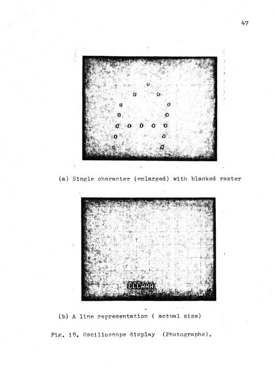
to generate one character is given in Appendix III. Photo
graphs of the oscilloscope display are shown in.fig. 18.
CHAPTER IV
IMPLEMENTATION
The character generator unit was implemented using
8
the DEC *R* series NAND logic modules, the logic levels being
0 and -3 volts. A few of the 'A1 series and *Wf series modu
les were employed wherever required.
The c.r.t. used for the display was a Tektronix
cathode ray oscilloscope with storage facilities. Since this
particular oscilloscope did not have a sawtooth output ter
minal, the vertical time base signal had to be obtained
from some other oscilloscope. The horizontal- time-base
circuit was designed and constructed as shown in fig.15.
The horizontal time-base circuit is an essentially
integrate and hold circuit constructed .using a Burr-Brown
operational amplifier as shown in fig. 15 a^d can be ana
lysed as follows:
For deriving the transfer function the following 9
assumptions can be made for an operational amplifier:'
1. Gain is infinite.
2. Input impedance is infinite.
3. Output impedance is zero.
The output occurs without any time lag.
5. The output voltage will be zero, when the input is zero.
33
SW 2
SW 1
A/W
Operational A m p l i f i e r ^
Fig.' 15. Horizontal deflection tine~ba.se circuit
Since the gain is almost infinite, if negative
feed, back is employed the potentials at.nodes 1 and 2 will
be the same. Refer to the fig.1 5 , When a capacitor is used
for the negative feed back the circuit acts like an integ
rator as can be shown mathematically.
By Kirchoff's current law at node 1 which is
approximately at 'O1 volts
- Yl / R = 0.dEo/dt
Hence - E Q = jvi/(CR)dt
Since Vj is a D.C.Voltage in our case
EQ = - V^t/(CR) + initial condition
As- the output voltage (maximum) EQ is specified
for the amplifier, any combinations of C and R can be used
to select the integrating time ’ t 1. If after a time * t£ *
less than *t 1 , the supply is disconnected the capacitor
will hold the voltage stored in it at that time, as it can
not discharge through the amplifier due to its high impeda
nce. Thus it generates the waveform required as shown in
fig. 6 (a).
Transistor switches numbered 2 and 3 are closed and the
switch number 1 is opened to reset the time-base output to
For the integration mode the switches 3 a^d 1 are closed
and the switch 2 is opened by the first clock pulse. For
hold conditions, the switches 1,2,3 are all opened by the
clock pulse number forty nine,thus achieving the synchroni
sm between the pulse train and the beam movement.
CHAPTER V
CONCLUSIONS ■ ■
Even though the character generator unit was
specifically constructed for the PDP-8/S computer, the
general principles used in the design and construction
can be extended to any interfaceable computer.
An attempt was made to set certain ’OR* gates
common for certain characters which have some common
pulses.to economise in the overall unit. But, since this
created certain changes in the logical functions, addi
tional gates were required to generate the desired func
tions, Thus it was found that the total cost did not
reduce to an appreciable extent. Though a slight reduction
in cost was evident, this idea was abandoned in favour
of the described scheme, since the latter afforded more
flexibility to change the shape of any character, if
required.
Due to the experimental nature of the project under
t a k e n ^ to test the concept of the method of character gene
ration), the gating circuitry was carried out for only 2
characters and the representation being carried out on one
line. However all the alpha-numeric characters can be
generated by providing the required character f0R* gates.
3
?
a digital to analog converter and an associated counter.
The analog output steps should be fed to the vertical
deflection plates along with the sawtooth voltage which
was used for the raster generation. The number of analog
step outputs should be equal to the number of lines desired.
This project could be further ext'ended by add
ing an additional input like a teletype and made more
flexible by incorporating a light-pen device.
APPENDIX I
THE OCTAL CODES USED FOR THE CHARACTER REPRESENTATION
Character
A B C ■ D E P G H 1 J K L M N 0 P Q R S T U V W X Y Z 0 1 2
3
if5
6 78
9- 39
Code used
01 02 03 Ok 05 06 07 10 11 12 13 lif 15 16 17 20 21 22 23 2 k 25 26 27 30 31 32 60 61 62
65
66
67
70 71e «••• ««« 0 *0* ••••
• • • * • o • • •
• • * • # 0 •
* * * 0 * * • » •*»
**♦« • • • • * •
• # 0 • • • » *
0 #•** #000
00*00 »•* 0 • 0
• * 0 0 * 0 0 * • e • 0 0
000 0 0 0 0 * 0 0 0
0 » * • • 0 0 0 0
0 0 0 0 * 0 0 0
• 000 0 0 * 0*0
ft ft ft • ft ftft ft ft ft
ft ft ft ft ft ft ftft ft ft ft
ft ft ft ft • * ft ft ft ft ft
ft ft ft ft ft ft ft ftft ft ft
ft ft ft ft ft ft ft ft •
ft ft •' ft ft ft ft ft ft
ft ft ft ft ft ft ft ft ft ft ft ft ft ft
0 0 0 0 0 0 0 0 0 0 * * 0 * 0 0 0 0 0
0 0 0 0 0 * 0 0 0
0 0 0 0 0 * 0 0
0 0 0 0 0 0 0 * 0 * *0 0 0
0 0 0 0 * 0 0 0
0 0 0 • « * * 0
0 0 0 0 * 0 ••* 0
ft ft ft ft ft • ft ft ■ ft ft
ft ft ft ft ft ft ft ft •- ft
ft ft ft ft ft ft ft ft ft ft ft
ft ft ft ft ft ft ft ft ft
ft ft ft ft ft ft ft ft ft ft
ft ft ft ft ft ft ft ft ft ft
ft ft ft ft ft ft ftft ft ft ft
0000 * * 0 0 * 0
0 * 0 0 0
00 0
0 0
* * 0
• ft ft >• %
• ft • • »
• ft
• ft ft
# • 9 • ft
ft
•
»
9 9 999
9 99 9 . •
9 99
9 9 0 9 9 9
9
9 9 ft • ft ft
ft ft ft 90
ft
ft ft ft ft ft ft
ft ft ft •
ft ft
ft * ft ft*
ft ft ft
ft ft ft
ft ft ft * ft ft ft ft ft ft ft
ft ft ft ft ft
ft ft
ft ft ft ft • ft «
ft ft ft
ft • •
ft ft ft ft ftft ftft
ft ft ft ft ft ft
Fig.l6 Proposed patterns for the characters
4 0
Ltt
7 f 1'+. .21. 28. 3-5.
6;,13. .2Q. 2?.. 3 ^
i . i
5;. I?. 19.
M
.3 4I!. 18. 25, .32,
3i 1 0 . 17. 2^ .31;
, : ; I
2i
9
*
164
23
i
30!
l;.8 . 15 ; 22i 29;
Pig. 17. Dot Matrix with reference Numbers
PULSE NUMBERS REQUIRED FOR THE FORMATION OF CHARACTERS
Character Pulse numbers
A 1,2,3 ,4,5,8 ,10,13,17,21, 24,27,29,30,31,32,33,
B 1,2,3,4,5,6,7,8,11,14,15,
1 8 ,21,22,28,30,31,33,3't
C 2,3,4,5,6,8,14,15,21,22,
28.30.34
D 1,2,3,4,5,6,7,8,14,15,21,
22.28.30.31.32.33.34
E 1,2,3,4,5,6,7,8,11,14,15,
18,21,22,28,29
F 1,2,3,4,5,6,7,11,14,18,21,
28,35
G 2,3,4,5,6,8,14,15,17,21,
22.24.28.30.31.34
H 1,2,3,4,5,6,7,11,18,25,29,
- 30,31,32,33,34,35
I 15,16,17,18,19,20,21
J 1,2,8,14,15,16,17,18,19,20, 21,28
K 1,2,3,4,5,6,7,11,17,19,23,
27.29.35
L 1,2,3,4,5,6,7,8,15,22,29
M 1,2,3,4,5,6,7,14,17,18,19,
28.29.30.31.32.33.34.35
N 1,2,3,4,5,6,7,13,19,25,29,
30,31,32,33,3^,35
Character P ulse numbers
P
Q
R
S
T
U
V
W.
X
Y
2 ,3 ,4,5,6,8,14,1 5 ,2 1 ,22, 28.30.31.32.33.34
1.2.3.4.5.6.7.11.14.18.21, 25.28.33.34
2,3,5.6,8.14,15,17.21,23, 28.29.31.32.33.34
1.2.3 .4.5.6.7.11.14.18.21, 24.25.28.29.30.33.34
2.5.6.8.11.14.15.18.21.22, 25.28.30.31.34
7,14,15,16,17,18,19,20,21, 28.35
2,3,4,5,6,7,8,15,22,30,31, 32.33.34.35
3,4,5,6,7,9,15,23,31,32,33,' 34.35
1,2,3,4,5,6,7,8,16,17,18, 19.22.29.30.31.32.33.34.35
1,2,6,7,10,12,18,24,26,29, 30.34.35
6.7.12.15.16.17.18.26.34.35
Z 1,2,7,8,10,14,15,18,21,22,26,
28,29,34,35
0 2,3,4,5,6,8,l2,l4,l5,l8, 2 1 .22.24.28.30.31.32.33.34
1 8,13,15,16,17,18,19,20,21,
22
2 1 ,6 ,8 ,9,1^,15,17,21,22,2 5 , 28.29.33.34
3 2,6,8,14,1 5 ,1 8 ,2 1 ,2 2 ,2 5 ,2 8 , 30.31.33.34
4 3,10,11,17,19,24,27,29,30,
31.32.33.34.35
5 2,5,6,7,8,12,14,15,19,21,
22.26.28.30.31.32.35
6 2,3,4,5,6,8,11,14,15,18,21,
22.25.28.30.31.34
7 1,7,9,14,17,21,25,28,33,
34.35
8 2,3,5,6,8,11,14,15,18,21,
22.25.28.30.31.33.34
9 2,5,6,8,11,14,15,18,21,22,
25.28.30.31.32.33.34
APPENDIX III
Plow chart for character generation
Is
Device ready No
Yes
/ Is character generation •^complete -No
Yes
Halt Start
Reset the beam
Transfer character for generation Bring character to accumulator
*200
CLA CLL
6334 /CHECK IF DEVICE IS READY
J M P . - l /IF NOT READY, CHECK AGAIN
6332 /IF READY, RESET THE BEAM
TAD A /BRING CHARACTER ’A' TO ACC
6331 / T R ANSFER CHARACTER AND START
C H A R A C T E R GENERATION' ON CRT
6334 /CHECK IF CHARACTER GENERATION
IS COMPLETE
JMP.-l /IF NOT C OMPLETE CHECK AGAIN
HLT A , 301 C, 303
$
47
(a) Single character (enlarged) with blanked raster
(b) A line representation ( actual size)
Fig. 1 8 . Oscilloscope display (Photographs).
LOGIC NOTATION
In the detailed analysis given in this thesis of
the operational sequences of character generator and PDP-8/S
it is assumed that the reader is familiar with the fundamen
tal concepts of logic and its notations. Many conventions
exist, however the particular set chosen for this write-up
is as follows:
SYMBOL FUNCTION AND A B DESCRIPTION
C = A.B
NAND
A
B
C = A.B
OR
A
B
C = A+B
NOT DELAY FLIP-FLOP A A N
Direct set Set level AC Set AC Reset Reset level Direct
clear-■B
— B
= D
-48
B = A
B = Delayed A
A
(See below) A
k9
■ FUNCTION SYMBOL DESCRIPTION
Set level AC set ONE-SHOT
The ON or SET output of the flip-flop is repre
sented. by 'A* and the OFF or RESET output is represented
by .'A*. When the flip-flop is set, A = 1 and A = 0 and
when the flip-flop is reset, A = 0 and A = 1.
A flip-flop can be set either through Direct set
input or by satisfying the AND gate fed by the set level
input and AC set. Similar choices exist for resetting the
the flip-flop also.
The following rules govern the use of flip-flops.
1. The AC set and the AC reset inputs respond only to a
logic level CHANGE from a ’O ’ to a *1 * state.
2. The Set level input (Reset level) be *1 * prior to the
activation of the AC set (AC reset) input if it is desi
red to operate the flip-flop.This lead time is equivale
nt to the memory time of the AND gate fed by these
inputs.
The ONE SHOT generates a pulse output of fixed
duration when triggered by the AC set input. The ,!X I? on its 0
input indicates this characteristic. 1
N /
/ \ 0 (See below)
REFERENCES
1. Corbin H.S., " A Survey of C.R.T. Display Consoles",
Control Engineering, Vol.12 No.l2,pp 77-83, Dec 1965.
2. Sloan W.R., " A High Speed Character Generator",
Electronic Industries,pp 17^-8^, Mar 196^.
3. Verdonk F.J.T.M., " Experimental Character Display
Unit using an Electro Static Cathode Ray Tube",
Electronic Applications, Vol.25 No.2 pp 6l-77
4. Boyd S.H., " Digital to Visible Character Generators",
Electro Technology, pp 77-88, Jan 1965.
5. Moore J.K. and Krohenberg M » , " Generating High Qua
lity Characters and Symbols", Electronics, Vol.33
PP 55, June 10, i960.
6 . Chao S.C., " Characters Displays Using Analog Tech
niques", Electronics, Vol.32 pp 11.6-18, Oct 23, 1959.
7. Staff of Digital Equipment Corporation., " A Small
Computer Handbook", Digital Equipment Corporation,
Maynard, Massachusetts
(1967).
8 . Staff of Digital Equipment Corporation., " A Logic
Handbook", Digital Equipment corporation, Maynard,
Massachusetts (l
966-67).
9. Staff of Burr-Brown Research Corporation., " A Hand
book on Operational Amplifier Applications",
Burr-Brown Research Corporation, Tucson, Arizona.
10. Wilson W.C., " Interfacing of Two Digital Computers",
University of Windsor, Master’s Thesis 1969.
11. Marcus, Mitchell P., " Switching Circuits for Engi
neers", Prentice-Hall Inc., 'Englewood Cliffs, New
Jersey (196?).
19^1
1957
1965
1969
VITA AUCTORIS
Born on September 25, in Bommidi, Madras, India.
Completed Secondary School Education at Municipal
High School, Gobichettipalayam, Madras, India.
Graduated from Osmania University, Hyderabad,
India, with the degree of B.E.(Hons) in Electrical
Engineering.
Candidate for the degree of M.A.Sc. in Electrical
Engineering at the University of Windsor.