University of Windsor University of Windsor
Scholarship at UWindsor
Scholarship at UWindsor
Electronic Theses and Dissertations Theses, Dissertations, and Major Papers
9-25-2018
Reliability Analysis and Optimization Models for Large Scale
Reliability Analysis and Optimization Models for Large Scale
Combinational Circuits
Combinational Circuits
Suoyue ZhanUniversity of Windsor
Follow this and additional works at: https://scholar.uwindsor.ca/etd
Recommended Citation Recommended Citation
Zhan, Suoyue, "Reliability Analysis and Optimization Models for Large Scale Combinational Circuits" (2018). Electronic Theses and Dissertations. 7591.
https://scholar.uwindsor.ca/etd/7591
This online database contains the full-text of PhD dissertations and Masters’ theses of University of Windsor students from 1954 forward. These documents are made available for personal study and research purposes only, in accordance with the Canadian Copyright Act and the Creative Commons license—CC BY-NC-ND (Attribution, Non-Commercial, No Derivative Works). Under this license, works must always be attributed to the copyright holder (original author), cannot be used for any commercial purposes, and may not be altered. Any other use would require the permission of the copyright holder. Students may inquire about withdrawing their dissertation and/or thesis from this database. For additional inquiries, please contact the repository administrator via email
Reliability Analysis and Optimization Models for Large
Scale Combinational Circuits
by
Suoyue Zhan
A Thesis
Submitted to the Faculty of Graduate Studies
through the Department of Electrical and Computer Engineering
in Partial Fulfillment of the Requirements for
the Degree of Master of Applied Science at the
University of Windsor
Windsor, Ontario, Canada
Reliability Analysis and Optimization Models for Large Scale Combinational Circuits
by
Suoyue Zhan
APPROVED BY:
______________________________________________ X.Nie
Department of Mechanical, Automotive and Materials Engineering
______________________________________________ S.Erfani
Department of Electrical and Computer Engineering
______________________________________________ C.Chen, Advisor
Department of Electrical and Computer Engineering
iii
DECLARATION OF ORIGINALITY
I hereby certify that I am the sole author of this thesis and that no part of this thesis has been published or submitted for publication.
I certify that, to the best of my knowledge, my thesis does not infringe upon anyone’s copyright nor violate any proprietary rights and that any ideas, techniques, quotations, or any other material from the work of other people included in my thesis, published or otherwise, are fully acknowledged in accordance with the standard referencing practices. Furthermore, to the extent that I have included copyrighted material that surpasses the bounds of fair dealing within the meaning of the Canada Copyright Act, I certify that I have obtained a written permission from the copyright owner(s) to include such material(s) in my thesis and have included copies of such copyright clearances to my appendix.
iv
ABSTRACT
With increasingly high density, today’s integrated circuit chips become sensitive to minor effects
such as temperature and environmental noises, which may lead to unreliable operation. While
circuit reliability can be improved at various design levels, this usually requires additional costs (such as more area and/or more power consumption). For large-scale circuits, the first step towards reliability improvement is to do reliability estimation efficiently and accurately. This is followed
by reliability optimization for given cost or budget constraints, which can be done either locally or globally.
In this thesis, we propose an asymmetrical reliability model (ARM) to do quick reliability estimation with a high level of accuracy, in comparison with true reliability values produced by Monte-Carlo simulations. Thanks to its linear-time complexity, this model can be well applied to
large-scale circuits. For instance, for benchmark circuit C7552 with 3512 logic gates, it only takes a few seconds to estimate the circuit output reliability with an average error of as low as 0.5%.
The only shortcoming of ARM model is that error-free signal probabilities are assumed to be available, which may not always be the case. This motivates us to develop another method to estimate both upper and lower bounds of circuit reliability regardless of signal probabilities.
It is also found that the actual average output reliability is strongly correlated with the average upper bound of reliability. This allows us to do fast analysis on circuit reliability with different
v
ACKNOWLEDGEMENTS
I would like to show my sincere appreciation to my academic supervisor Dr. Chunhong Chen for his guidance and support during my Master Program.
I would like to thank Dr. Xueyue Nie and Dr. Shervin Erfani for providing precious feedbacks.
I am grateful to Ms. Andria Turner for her administrative assistance.
Finally,I would like to thank my parents: Zheng He, Yi Zhan, and stepparents Xiaojun Zhang,
Limin Jiang for their love and support on my study and life.
vi
TABLE OF CONTENTS
DECLARATION OF ORIGINALITY ... iii
ABSTRACT ... iv
ACKNOWLEDGEMENTS ... v
LIST OF FIGURES ... viii
LIST OF TABLES ... ix
CHAPTER 1. INTRODUCTION ... 1
1.1 Background ... 1
1.2 Previous work ... 1
1.3 Organization of Thesis ... 2
CHAPTER 2. ASYMMETRICAL RELIABILITY MODEL ... 4
2.1 Reliability Asymmetry ... 4
2.2 Signal Correlation ... 7
2.3 Propagation of Conditional Reliabilities ... 9
2.3.1 Independent Case ... 9
2.3.2 Full-Correlation Case ... 10
2.3.3 General Case ... 12
2.3.4 Other Considerations ... 16
2.4 Time Complexity ... 17
2.5 Simulation Results ... 17
CHAPTER 3. ESTIMATION OF RELIABILITY BOUNDS ... 20
3.1 Upper and Lower Bounds ... 20
3.2 Propagation of Conditional Reliability Bounds ... 25
3.3 Algorithm for Reliability Bounds ... 29
vii
CHAPTER 4. RELIABILITY ALLOCATION ... 33
4.1 Budget ... 33
4.2 Allocation Model ... 34
4.3 Simulation results... 38
CHAPTER 5. CONCLUSION AND FUTURE WORK ... 39
5.1 Conclusion ... 39
5.2 Future work ... 39
APPENDIX 1. IMPORTANT CODES ... 40
Reliability Estimation ... 40
Reliability Bounds ... 49
Reliability Allocation ... 57
REFERENCES ... 63
viii
LIST OF FIGURES
Figure 2-1………...8
Figure 2-2………...9
Figure 2-3……….11
Figure 2-4……….16
Figure 2-5……….17
Figure 3-1……….23
Figure 3-2……….24
Figure 3-3……….25
Figure 3-4……….33
Figure 3-5……….34
Figure 4-1……….37
Figure 4-2……….38
ix
LIST OF TABLES
Table 2-1………8
Table 2-2………..20
Table 2-3………..21
Table 2-4………..21
Table 4-1………..36
1
CHAPTER 1. INTRODUCTION
1.1 Background
As electronic device size keeps shrinking, integrated circuits are becoming more sensitive to unexpected effects (such as temperature variation and background noises), which lead to unreliable
operation. While it is generally true that the higher component reliabilities can promise more reliable circuits, this comes at exponentially increasing costs (including more area penalty and/or higher power consumption). Therefore, it is necessary to have a preview of component reliability
assignment under certain cost or budget constraints, before an efficient output reliability evaluation is conducted. If the circuit could not meet the reliability requirement otherwise, a costly redesign
process would be needed.
For digital combinational circuits, the only components considered are logic gates, assuming all wire connections are 100% reliable. Then the problem becomes: 1. How to do general allocation
of logic gate reliabilities before the design within certain budgets. 2. How to evaluate output reliabilities after the design accurately and efficiently.
1.2 Previous work
As for reliability estimation, researchers have already done a lot of work which provide fast and approximate results, as reported in [1]. Monte-Carlo simulation is considered as a typical method for circuit performance estimation and reliability evaluation, but it is computationally expensive
2
gate model (PGM) [5], probability transfer matrix (PTM) [6], conditional probability matrix (CPM)
[7], Bayesian network 8], and Boolean difference-based error calculator (BDEC) [9]. Readers are referred to [9] for a review of related work on this topic.
References [10] and [11] introduced certain algorithms on reliability bounds estimation within
acceptable accuracy and tolerance. The time complexity of these algorithms, however, is not strictly linear to the number of gates. [12] presented some further discussions on the effects of
input vector probabilities on circuit reliability.
Due to the fact that reliability allocation is aiming at maximizing the output reliability within certain constraints such as cost or area, [13,14,15] produced certain models for reliability
optimization, taking into considerations three masking issues (i.e., logic masking, electrical masking and time masking), and provided local solutions by gate resizing and partial circuit restructuring.
1.3 Organization of Thesis
The organization of thesis is as follows.
Chapter 2 presents a new asymmetrical reliability model (ARM) to deal with the reliability
estimation issue with high accuracy level and linearly increasing processing time proportional to circuit size, assuming the error-free nodes probability are already available. Comparison of PGM
and ARM are also shown in this chapter by MATLAB simulation.
Chapter 3 focuses on further improvement of efficiency by relaxing the requirements of ARM model. Without knowing the error-free signal reliabilities, people are still able to achieve reliability
bounds estimation for a quick look at circuit performance. The bounds are verified to be a true
3
Chapter 4 is devoted to reliability allocation issues before completing the design. By taking
advantage of the fact that real average output reliabilities are proportional, though not strictly, to average output upper bounds, we derive a fast, near-optimal allocation model which allows further modifications for a better performance.
4
CHAPTER 2. ASYMMETRICAL
RELIABILITY MODEL
2.1 Reliability Asymmetry
For any signal s in a circuit, its probability is defined as Ps = Pr{s = “1”}, and its reliability rs is defined as the probability that it generates an intended logic value, i.e., rs = Pr{s = s*}, where s* is
the error-free version of s. Throughout this paper, the symbol “*” is used to indicate “error-free”.
If s is a primary output of the circuit, then rs represents the reliability of this output signal. Similarly, for a logic gate g, its reliability (denoted by rg) is defined as the probability that an
intended output logic value is produced for given input signals.
Considering the probability of error-free signal s*, we express the reliability rs as:
rs = Pr{s = s*}
= Pr{s = ‘1’ ∩ s* = ‘1’} + Pr{s = ‘0’ ∩ s* = ‘0’}
= Pr{s = ‘1’| s* = ‘1’}∙Ps* + Pr{s = ‘0’| s* = ‘0’}∙(1─ Ps*)
= ks∙Ps* + ls∙(1─ Ps*) (2-1)
where
𝑘𝑠 = 𝑃𝑟{𝑠 =′1′|𝑠∗ = ′1′}
𝑙𝑠 = 𝑃𝑟{𝑠 =′1′|𝑠∗ = ′1′}} (2-2)
which represent conditional reliabilities (or probabilities) for ‘1’ patterns and ‘0’ patterns,
respectively. In other words, the reliability of any signal s is associated with a pair of conditional
5
documented in literature [4, 10, 11], and is beyond the scope of our discussions. For small circuits,
the conditional reliabilities {ks, ls} for any signal can be found using Monte-Carlo simulations. As
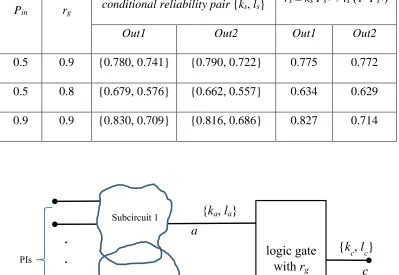
an example, Fig. 2-1 shows the schematic of circuit Benchmark Circuit C17 with six 2-input
NAND gates, where all primary inputs (i.e., signals #1~#5) are assumed to be independent and
reliable. Table 2-1 shows some of our simulation results for the conditional reliability pairs at both output signals Out1 and Out2 assuming different primary input probabilities (Pin) and gate
reliability (rg). It can be seen from the table that ks and ls have different values (i.e., signal
reliabilities are asymmetrical in general), which vary with input signal probabilities and/or gate
reliabilities. For the signal Out2 with Pin = 0.9 and rg = 0.9 in particular, ks and ls differ by more
than 15%.
For large circuits with potential signal correlations, it would be impractical to find ks and ls directly
and accurately by using an exhaustive and time-consuming approach. This is because both of those parameters depend on input signal probabilities, signal correlations, as well as gate reliabilities.
However, with some approximation, the values of both ks and lscan be propagated gate by gate
throughout the circuit, as detailed in the next section. This will make the reliability estimation very
efficient with the time complexity linear to circuit size N (i.e., the number of gates). The main
challenge here is, among other things, how to capture signal correlations while propagating ks and
6
Figure 2-1. Example circuit C17.
Table 2-1. Asymmetric Conditional Reliabilities with C17
Pin rg conditional reliability pair {ks, ls}
rs = ks∙Ps* + ls∙(1−Ps*)
Out1 Out2 Out1 Out2
0.5 0.9 {0.780, 0.741} {0.790, 0.722} 0.775 0.772
0.5 0.8 {0.679, 0.576} {0.662, 0.557} 0.634 0.629
0.9 0.9 {0.830, 0.709} {0.816, 0.686} 0.827 0.714
Figure 2-2. General logic gate with two correlated inputs.
1
2
3
4
5
G
1G
2G
4G
3G
6G
56
7
8
9
11
10
ubcircuit 1
ubcircuit 2
logic gate with
PIs
, }
{kb, lb}
a
b
{k c, lc}
c
7
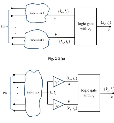
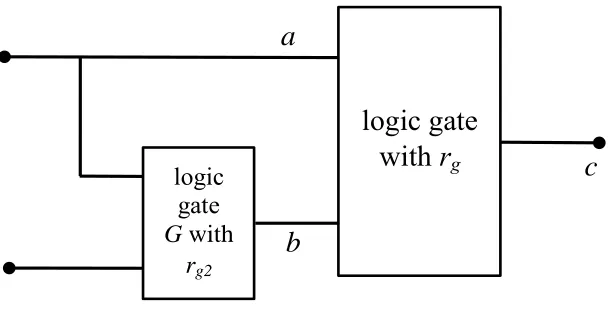
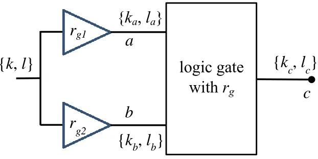
2.2 Signal Correlation
Consider a two-input logic gate (with gate reliability of rg) in any combinational circuit, as shown
in Fig. 2-2 where a, b and c denote the two input signals and one output, respectively. They are
associated with conditional reliabilities {ka, la}, {kb, lb} and {kc, lc}, respectively. For the two error-free signals a* and b* (i.e., signals a and b when all gate reliabilities are 1), we define an error-free
probability vector P* = [P00* P01* P10* P11*] = [Pr{a*b*= 00} Pr{a*b*= 01} Pr{a*b*=10}
Pr{a*b*=11}]. In order to deal with signal correlations, from [16], we take signal correlation factor
between a* and b* as:
𝜃𝑖𝑗 = 𝑃𝑟{𝑎
∗𝑏∗=𝑖𝑗}−𝑃𝑟{𝑎∗=𝑖}∙𝑃𝑟{𝑏∗=𝑗}
√𝑃𝑟{𝑎∗=𝑖}∙𝑃𝑟{𝑏∗=𝑗}(1−𝑃𝑟{𝑎∗=𝑖})∙(1−𝑃𝑟{𝑏∗=𝑗}) (2-3)
where −1 ≤ θij ≤ 1 with i, j = 0 or 1. The positive or negative sign of θij represents a positive or
negative signal correlation. Both P* and θ
ij can be found using error-free signal probabilities (i.e.,
Pa*, Pb* and Pc*) at both inputs and output of the gate, depending on the gate type. For instance, if
the gate is a NAND gate, P*= [2−P
a*−Pb*−Pc* Pb*+Pc*−1 Pa*+Pc*−1 1−Pc*], and
) 1 ( ) 1 ( / ) 1
( * * * * * * *
10 01 11
00 θ θ θ Pc PaPb Pa Pa Pb Pb
θ . Again, take C17 of Fig. 1 for example. Assuming
primary input probabilities of 0.5, we found Pa* = P6* = 0.750, Pb* = P8* = 0.625 and Pc* = Pout1* =
0.563 for signals #6 and #8 (i.e., two inputs of NAND gate G5 in Fig. 2-1), and thus P*= [0.063
0.188 0.312 0.437] and |θij| ≈ 0.148. For input signals #8 and #9 of NAND gate G6 with stronger
correlation, it is found that Pa* = P8* = 0.625, Pb* = P9* = 0.625 and Pc* = Pout2* = 0.563, which lead
to P*= [0.188 0.188 0.187 0.437] and |θ
ij| ≈ 0.2. Generally speaking, 0 ≤ |θij| ≤ 1, and the signal correlation gets stronger as the value of |θij| increases. However, special attention shall be given to two extreme cases where θij = 0 or |θij| = 1. The former case happens if both a* and b* are
8
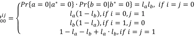
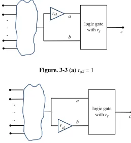
and (b), respectively, where rg1 and rg2 denote the reliability of two buffers.
Fig. 2-3 (a)
Fig. 2-3 (b)
Figure 2-3. Logic gate with independent inputs (a) and full-correlation inputs (b).
ubcircuit 1
ubcircuit 2
logic gate with
PIs
, }
{kb, lb}
a
b
{kc, lc}
c
.
.
.
ubcircuit logic gate
with
PIs
, }
{kb, lb}
a
b
{kc, lc}
c
.
.
.
rg1
rg2
9
2.3 Propagation of Conditional Reliabilities
Propagation of conditional reliability pairs for the gate of Fig. 2-2 can be done by finding {kc, lc}
for given {ka, la} and {kb, lb}. If this is done, all conditional reliabilities at this circuit’s outputs can
be found by repeating the propagation process for all N gates in a topological order. The output
reliabilities are finally given by (2-1). In the following sections, we first look at the two extreme
cases in Fig. 2-3, and then extend our results to the general case of Fig. 2-2.
2.3.1 Independent C se
Before discussing conditional reliabilities, it would be necessary to begin with a specific
conditional probability ij
P00= Pr{ab = ij | a
*b*=00}, where i, j = 0 or 1. For the independent case of
Fig. 2-3 (a) with θij = 0, we have
𝑃00𝑖𝑗 = {
𝑃𝑟{𝑎 = 0|𝑎∗ = 0} ∙ 𝑃𝑟{𝑏 = 0|𝑏∗ = 0} = 𝑙
𝑎𝑙𝑏, 𝑖𝑓𝑖 = 𝑗 = 0
𝑙𝑎(1 − 𝑙𝑏), 𝑖𝑓𝑖 = 0, 𝑗 = 1
𝑙𝑏(1 − 𝑙𝑎), 𝑖𝑓𝑖 = 1, 𝑗 = 0 1 − 𝑙𝑎− 𝑙𝑏+ 𝑙𝑎∙ 𝑙𝑏, 𝑖𝑓𝑖 = 𝑗 = 1
(2-4)
Similarly, we can find ij
P01= Pr{ab = ij | a
*b*=01}, ij
P10= Pr{ab = ij | a
*b*=10}, or ij
P11=Pr{ab = ij |
a*b*=11} with the above la and lb in (2-4) being replaced by la and kb, ka and lb, or ka and kb,
respectively. For instance, ij
P01is expressed as
𝑃01𝑖𝑗 =
{
𝑙𝑎(1 − 𝑘𝑏), 𝑖𝑓𝑖 = 𝑗 = 0
𝑃𝑟{𝑎 = 0|𝑎∗ = 0} ∙ 𝑃𝑟{𝑏 = 1|𝑏∗ = 1} = 𝑙
𝑎𝑘𝑏, 𝑖𝑓𝑖 = 0, 𝑗 = 1
(1 − 𝑙𝑎)(1 − 𝑘𝑏), 𝑖𝑓𝑖 = 1, 𝑗 = 0 (1 − 𝑙𝑎)𝑘𝑏, 𝑖𝑓𝑖 = 𝑗 = 1
(2-5)
In other words, we can obtain a 4×4 conditional probability matrix (for input signals a and b) as
10 𝑀 =
[
𝑃0000 𝑃0001 𝑃0010 𝑃0011
𝑃0100 𝑃
0101 𝑃0110 𝑃0111
𝑃1000 𝑃
1001 𝑃1010 𝑃1011
𝑃1100 𝑃1101 𝑃1110 𝑃1111]
= [ 𝑀00
𝑀01 𝑀10
𝑀11
] (2-6)
with . 1 , 11 , 10 , 01 ,
00
j i ij j i ij j i ij j i ij P P P
P With the availability of M and P
*, k
c and lc in Fig. 3 (a) can be found
analytically, depending on the gate type. For example, if the logic gate in Fig. 3 (a) is an NAND gate, then we have
𝑘𝑐= 𝑃𝑟{𝑐 =′1′|𝑐∗=′1′} = [𝑃00∗ 𝑃01∗ 𝑃10∗] ∙ [ 𝑀00 𝑀01 𝑀10
] ∙ [𝑟𝑔 𝑟𝑔 𝑟𝑔 1 − 𝑟𝑔]𝑇/(1 − 𝑃11∗ )
𝑙𝑐= 𝑃𝑟{𝑐 =′0′|𝑐∗=′0′} = 𝑀11∙ [1 − 𝑟𝑔 1 − 𝑟𝑔 1 − 𝑟𝑔 𝑟𝑔]𝑇
} (2-7)
For any other gates, the conditional reliability pair {kc, lc} can be found in a similar way.
2.3.2 Fu -Co e tion C se
For the full-correlation case (|θij| = 1) of Fig. 3 (b) where {k, l} is the conditional reliability pair of buffer’s input, we have
𝑙𝑎= 𝑙 ∙ 𝑟𝑔1+ (1 − 𝑙)(1 − 𝑟𝑔1) 𝑙𝑏 = 𝑙 ∙ 𝑟𝑔2+ (1 − 𝑙)(1 − 𝑟𝑔2)
} (2-8)
Assuming rg1 and rg2 are independent, the conditional probability P0000is given by
𝑃0000= 𝑙 ∙ 𝑟𝑔1∙ 𝑟𝑔2+ (1 − 𝑙)(1 − 𝑟𝑔1)(1 − 𝑟𝑔2) (2-9)
11
(2-9) gives
𝑃0000≈ 𝑚𝑖𝑛{𝑙𝑎∙ 𝑟𝑔2− ∆𝑎00, 𝑙𝑏∙ 𝑟𝑔1− ∆𝑏00} (2-10)
where
∆𝑎00=(1 − 𝑙𝑎)(1 −𝑟𝑔1)(2𝑟𝑔2− 1) ∆𝑏00=(1 − 𝑙𝑏)(1 −𝑟𝑔2)(2𝑟𝑔1− 1)
} . (2-11)
The conditional probability ij
P00is expressed as
𝑃01𝑖𝑗 =
{
𝑃0000, 𝑖𝑓𝑖 = 𝑗 = 0
𝑙𝑎− 𝑃0000, 𝑖𝑓𝑖 = 0, 𝑗 = 1
𝑙𝑏− 𝑃0000, 𝑖𝑓𝑖 = 1, 𝑗 = 0
1 − 𝑙𝑎− 𝑙𝑏+ 𝑃0000, 𝑖𝑓𝑖 = 𝑗 = 1
(2-12)
where 00
00
P is given by (2-10). It can be proved that the value ofP0000 is greater than or equal to la∙lb,
but less than or equal to either la or lb. This ensures that 0 ≤P00ij≤ 1 in (2-12). Also, if the values of
rg1, rg2, la, lb, ka and kb are all between 0.5 and 1, which is the case in general, thenP00ij≤ 00 00
P for i, j =
0 or 1. Similarly, we can find ij
P01, ij
P10, or ij
P11 with the above la and lb in (2-10), (2-11) and (2-12)
being replaced by la and kb, ka and lb, or ka and kb, respectively. For instance, P01ijis expressed as
𝑃01𝑖𝑗 =
{
𝑙𝑎− 𝑃0101, 𝑖𝑓𝑖 = 𝑗 = 0
𝑃0101, 𝑖𝑓𝑖 = 0, 𝑗 = 1
1 − 𝑙𝑎− 𝑘𝑏+ 𝑃0101, 𝑖𝑓𝑖 = 1, 𝑗 = 0
𝑘𝑏− 𝑃0101, 𝑖𝑓𝑖 = 𝑗 = 1
(2-13)
where 01
01
12
𝑃0101≈ 𝑚𝑖𝑛{𝑙𝑎∙ 𝑟𝑔2− ∆𝑎01, 𝑙𝑏∙ 𝑟𝑔1− ∆𝑏01} (2-14)
and
∆𝑎01=(1 − 𝑙𝑎)(1 −𝑟𝑔1)(2𝑟𝑔2− 1) ∆𝑏01=(1 − 𝑘𝑏)(1 −𝑟𝑔2)(2𝑟𝑔1− 1)
} (2-15)
and 0 ≤ ij
P01≤ 1. By comparing (2-4)~(2-5) and (2-10)~(2-15), one can see that when it comes to
propagation of conditional reliabilities, the only difference between Fig. 3 (a) and (b) is the way to calculate the matrix M in (2-6). Eq. (2-7) for calculating {kc, lc} always works regardless of signal correlations.
There are two other full-correlation cases which are worth mentioning, as shown in Fig. 2-4. For the case of Fig. 4 (a) where the inputs a and b are connected to a same signal, we have: rg1 = rg2
=1, la = lb and ka = kb. Thus, P0000= la andP1111= ka. However, bothP01ijand
ij
P10are immaterial because
P01*=P10* = 0 in this case. On the other hand, for the case of Fig. 4 (b) where rg2 =1, we haveP0101≈
min{ la−(1−la)(1−rg1), kb∙rg1} andP1010≈ min ka−(1−ka)(1−rg1), lb∙rg1}, while both
ij
P00and
ij
P11are
immaterial in this particular case due to P00*=P11*= 0. Both cases of Fig. 4 rarely appear in a circuit
implementation. However, even if they do, they can be identified during the reliability propagation with proper setting for rg1 and/or rg2, as mentioned above.
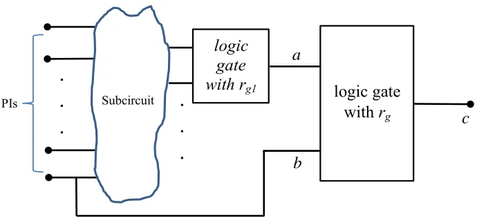
2.3.3 Gene C se
The general case of signal correlations is illustrated in Fig. 2-2, where the correlation factor θij of
(2-3) stays somewhere in between the above extreme cases (i.e., 0 < |θij| < 1). The key issue in
finding all elements in M of (2-6) for this case is to calculate its diagonal elements (i.e., ij
ij
P , i, j =
0 or 1). Unfortunately, an exact value of ij
ij
13
However, based on the above discussions with independent and full-correlation cases, ij
ij
P for the
general case can be approximated as follows:
𝑃0000 = 𝑙
𝑎∙ 𝑙𝑏+ 𝜃002 ∙ (𝑚𝑖𝑛{𝑙𝑎∙ 𝑟𝑔2− ∆𝑎00, 𝑙𝑏∙ 𝑟𝑔1− ∆𝑏00}− 𝑙𝑎𝑙𝑏) 𝑃0101 = 𝑙
𝑎∙ 𝑘𝑏+ 𝜃012 ∙ (𝑚𝑖𝑛{𝑙𝑎∙ 𝑟𝑔2− ∆𝑎01, 𝑘𝑏∙ 𝑟𝑔1− ∆𝑏01}− 𝑙𝑎𝑘𝑏) 𝑃1010 = 𝑘
𝑎 ∙ 𝑙𝑏+ 𝜃102 ∙ (𝑚𝑖𝑛{𝑘𝑎∙ 𝑟𝑔2− ∆𝑎10, 𝑙𝑏∙ 𝑟𝑔1− ∆𝑏10}− 𝑘𝑎𝑙𝑏) 𝑃1111 = 𝑘
𝑎∙ 𝑘𝑏+ 𝜃112 ∙ (𝑚𝑖𝑛{𝑘𝑎∙ 𝑟𝑔2− ∆11𝑎 , 𝑘𝑏∙ 𝑟𝑔1− ∆𝑏11}− 𝑘𝑎𝑘𝑏)}
(2-16)
where ∆a00 = ∆a01, ∆a10 = ∆a11, ∆b00 =∆b10, and ∆b01 = ∆b11. ThePijijfor the independent case (refer to
(2-4) and (2-5)) or full-correlation case (refer to (2-10) and (2-14)) is a special case of (2-16) when |θij| = 0 or 1. The positive or negative signal correlation (i.e., the sign of θij) is taken into account
by using the conditional reliability pairs of {ka, la} and {kb, lb}.
Figure 2-4 (a)
logic gate
with
,
}
a
b
{
k
c
,
l
c}
14
Figure 2-4 (b)
Figure 2-4. Two special cases with full-correlation signals.
Figure 2-5 (a) rg2 = 1.
logic gate
with
,
}
{
k
b,
l
b}
a
b
{
k
c,
l
c}
c
r
g1ubcircuit logic gate
with
PIs
o i te it 1
a
b
c
.
.
.
15
Figure 2-5 (b) rg1 = 1.
Figure 2-5. Considerations for two special input signals.
Once ij
ij
P is available with i, j = 0 or 1, all off-diagonal elements in M of (2-6) can be obtained with
help of {ka, la} and {kb, lb} (for example, using (2-12) and (2-13) forP00ijandP01ij, respectively). With
the availability of M, P* and gate type, the conditional reliability pair {kc, lc} at the gate output can be found (refer to (2-7) for instance). Results reported in Section 4 show that the accuracy level of (2-16) is very high with an average error of typically 2% in estimating the circuit reliability,
depending on specific circuits and gate reliabilities.
It should be noted that in addition to considerations for the two cases of Fig. 2-4, (2-16) shall be
modified under other two cases: i) If one of the two inputs a (or b) in Fig. 2-2 is a primary input
(refer to Fig. 2-5 (a) where b is a primary input), one shall let rg1 = 1 (or rg2 = 1) in (2-16) with the
assumption that all primary inputs are reliable; ii) If the two signals a and b happen to be an input
and output of a same gate, one shall also let rg1 = 1 as shown in Fig. 2-5 (b), where the signal a is
an input of gate G while the signal b is the output of gate G. In case both signals a and b in Fig.
2-logic gate
with
a
b
c
logicgate
G with
16
2 are primary inputs, we have |θij| = 0 for i, j = 0 or 1 (assuming all primary inputs are independent),
and thus (2-16) gives a same value of ij
ij
P regardless of rg1 and rg2.
2.3.4 Ot e Conside tions
In the above analysis, we only deal with 2-input gates. For an inverter with input a and output c, the conditional reliabilities at the output are simply expressed as
𝑘𝑐 = 𝑟𝑔∙ 𝑙𝑎+ (1 − 𝑟𝑔)(1 − 𝑙𝑎)
𝑙𝑐 = 𝑟𝑔 ∙ 𝑘𝑎+ (1 − 𝑟𝑔)(1 − 𝑘𝑎)} (2-17)
where rg is the gate reliability and {ka, la} is the conditional reliability pair at the input. For a logic
gate with q inputs (q > 2), the conditional probability matrix M will be in size of 2q×2q, and
involves the signal correlations among q inputs. While our model could be extended theoretically to this case, the propagation of conditional reliabilities would become much more complicated. A quick solution instead is to decompose the gate into a few two-input gates (e.g., decomposition of
3-input AND gate to two 2-input gates). Fortunately, majority of gates in real-world circuits have no more than two inputs, and most logic synthesis tools also provide an option of doing the
decomposition with 2-input gates only. Further discussions on handling multi-input gates are beyond the scope of this work.
It should also be mentioned that when analyzing circuit reliability, one needs to consider electrical
masking, temporal masking and logic masking in general. Electrical masking shall be included in
evaluating gate reliability rg which is assumed to be available in this work, and temporal masking
shall be considered in sequential circuits which are not discussed here. The focus of this work is to deal with logic masking, signal correlations as well as their roles in determining the reliability
17
output of a gate are always less than or equal to the gate reliability (rg), they could be greater than
the conditional reliabilities (ka, la, kb or lb) at inputs of the gate due to logic masking and/or input signal correlations. In other words, the output signal reliability for a gate could be higher than its input reliabilities if rg is relatively large. Therefore, when signal reliabilities propagate through the
whole circuit, they may not necessarily diminish, or at least not do as quickly as one might think.
2.4 Time Complexity
The asymmetric reliability model (ARM) presented in the previous section allows us to derive any logic gate’s output reliability directly from the conditional reliabilities at its inputs. This makes the
circuit reliability analysis significantly fast with O(N) time complexity (assuming the availability
of error-free signal probabilities), where N is the total number of gates in the circuit. This analysis
efficiency is important not only for large circuits, but also for repeated reliability evaluations with different gate reliabilities which are required for reliability improvement/optimization. The model
is also able to take signal correlations into account without the need for exhaustively exploring the potential impacts of all transitive fan-ins on the circuit output reliability. This is possible mainly
by introducing the asymmetrical reliability pair {k, l} as well as using the approximation in (2-16).
2.5 Simulation Results
Table 2-2 and Table 2-3 show the detailed results for every single output regarding to benchmark circuit C17. The Monte-Carlo results are calculated with 107 iterations, which is considered as
18
higher gate reliability will provide a more accurate result. Therefore, in the following simulations,
we simply put input vector to be Pin = 0.5
Table 2-2. Simulation results on output reliabilities for C17 with rg = 0.99 and different
values of Pin
Output
Signal
Pin = 0.1 Pin = 0.5 Pin = 0.9
ARM MC ARM MC ARM MC
Out1 0.971 0.971 0.973 0.973 0.980 0.980
Out2 0.971 0.971 0.973 0.971 0.965 0.965
Average error 0.0% 0.1% 0.0%
Table 2-3. Simulation results on output reliabilities for C17 with Pin = 0.5 and different
values of rg
Output Signal
rg = 0.9 rg = 0.99 rg = 0.999
ARM MC ARM MC ARM MC
Out1 0.775 0.775 0.973 0.973 0.997 0.997
Out2 0.772 0.760 0.973 0.971 0.997 0.997
19
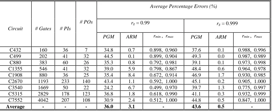
Table 2-4. Comparison of Average Estimation Errors (%) for Reliability Analysis on
Benchmark Circuits (Pin = 0.5)
Circuit # Gates # PIs
# POs
Average Percentage Errors (%)
rg = 0.99 rg = 0.999
PGM ARM rmin , rmax PGM ARM rmin , rmax
C432 160 36 7 34.8 0.7 0.898, 0.960 37.6 0.1 0.988, 0.996 C499 202 41 32 44.5 0.1 0.899, 0.904 49.3 0.0 0.987, 0.989 C880 383 60 26 35.3 0.8 0.792, 0.981 39.1 0.1 0.973, 0.998 C1355 546 41 32 39.0 5.9 0.798, 0.867 48.4 0.6 0.964, 0.978 C1908 880 36 25 35.4 8.4 0.672, 0.914 46.9 1.7 0.930, 0.985 C2670 1193 233 140 43.4 1.1 0.592, 1.000 45.1 0.2 0.905, 1.000 C3540 1669 50 22 24.2 6.7 0.499, 0.970 39.7 1.3 0.775, 0.997 C5315 2829 178 123 36.8 1.8 0.618, 0.990 41.1 0.3 0.932, 0.999 C7552 4042 207 108 30.9 2.4 0.512, 1.000 44.8 0.5 0.847, 1.000
Average - - - 36.0 3.1 - 43.6 0.5 -
The overall error comparing to MC value is far less than PGM. The reason is that PGM provide very high error when output reliability is approaching 0.5, especially the case in large circuit such
20
CHAPTER 3. ESTIMATION OF
RELIABILITY BOUNDS
3.1 Upper and Lower Bounds
Consider a generic logic gate with output c and two inputs a and b, as shown in Fig. 3-1 where rg
is the gate reliability, and {ka, la}, {kb, lb} and {kc, lc} represent the conditional reliability pair for signals a, b and c, respectively. We define a conditional probability for the two inputs (i.e., a and
b) as follows:
𝑃𝑖𝑗𝑢𝑣= Pr{′𝑎𝑏′ = ′𝑢𝑣′|′𝑎∗𝑏∗′ = ′𝑖𝑗′} (3-1)
where i, j, u, v = ‘0’ or ‘1’, and a* and b* are an error-free version of a and b, respectively. This
conditional probability can be expressed as
𝑃𝑖𝑗𝑢𝑣 =
{
𝑃𝑖𝑗𝑖𝑗, 𝑖𝑓𝑢 = 𝑖𝑎𝑛𝑑𝑣 = 𝑗 𝑞𝑎− 𝑃𝑖𝑗𝑖𝑗, 𝑖𝑓𝑢 = 𝑖𝑎𝑛𝑑𝑣 ≠ 𝑗
𝑞𝑏− 𝑃𝑖𝑗𝑖𝑗,𝑖𝑓𝑢 ≠ 𝑖𝑎𝑛𝑑𝑣 = 𝑗 1 − 𝑞𝑎− 𝑞𝑏+ 𝑃𝑖𝑗𝑖𝑗, 𝑖𝑓𝑢 ≠ 𝑖𝑎𝑛𝑑𝑣 ≠ 𝑗
(3-2)
where
𝑞𝑎 = {𝑙𝑎, 𝑖𝑓𝑖 = ′0′
𝑘𝑎, 𝑖𝑓𝑖 = ′1′ and 𝑞𝑏 = {
𝑙𝑏, 𝑖𝑓𝑗 = ′0′
𝑘𝑏, 𝑖𝑓𝑗 = ′1′ (3-3)
with 𝑃𝑖𝑗00+ 𝑃𝑖𝑗01+ 𝑃𝑖𝑗10+ 𝑃𝑖𝑗11 = 1.
21
correlations between a and b. However, its bounds can be estimated by considering the following
two extreme cases: (1) signals a and b are fully-independent, and (2) they are fully-correlated. Let
us take 𝑃0000 for example. Under this independent case, we have 𝑃0000 = 𝑙𝑎𝑙𝑏. The value of 𝑃0000
increases as signals a and b get more correlated and reaches its maximum when they are
fully-correlated. A general case of full-correlation is illustrated in Fig. 3-2 where both a and b are driven
by a buffer with reliability of rg1 and rg2, respectively. We have
Figure 3-1. A generic 2-input logic gate.
Figure 3-2. A general case of full correlation between two signals a and b.
logic gate
with
,
}
{
k
b,
l
b}
a
b
{
k
c,
l
c}
c
logic gate
with
,
}
{
k
b,
l
b}
a
b
{
k
c
,
l
c}
c
r
g122
𝑙𝑎= 𝑙 ∙ 𝑟𝑔1+ (1 − 𝑙)(1 − 𝑟𝑔1)
𝑙𝑏= 𝑙 ∙ 𝑟𝑔2+ (1 − 𝑙)(1 − 𝑟𝑔2)} (3-4)
where 0 ≤ 𝑙 ≤ 1 (refer to Fig. 3-2). Since rg1 and rg2 are independent, the conditional probability
𝑃0000 is given by
𝑃0000= 𝑙 ∙ 𝑟𝑔1∙ 𝑟𝑔2+ (1 − 𝑙)(1 − 𝑟𝑔1)(1 − 𝑟𝑔2) (3-5)
Combination of (3-4) and (3-5) gives
𝑃0000= 𝑙
𝑎∙ 𝑟𝑔2−
𝑟𝑔1− 𝑙𝑎
2𝑟𝑔1− 1(1 − 𝑟𝑔1)(2𝑟𝑔2− 1),
or
𝑙𝑏∙ 𝑟𝑔1− 𝑟𝑔2−𝑙𝑏
2𝑟𝑔2−1(1 − 𝑟𝑔2)(2𝑟𝑔1− 1) . (3-6)
Since the typical value of rg1 or rg2 is close to 1, the second term in (3-6) would be negligibly small.
Thus, we have
𝑃0000≤ 𝑙
𝑎∙ 𝑟𝑔2, 𝑜𝑟𝑃0000≤ 𝑙𝑏∙ 𝑟𝑔1 . (3-7)
In order to ensure 0 ≤ 𝑃00𝑢𝑣≤ 1, where 𝑃
00𝑢𝑣is given by (3-2) with u, v = 0 or 1, the value of 𝑃0000 is no greater than min{𝑙𝑎∙ 𝑟𝑔2, 𝑙𝑏∙ 𝑟𝑔1}. In other words, 𝑃0000 is bounded as:
𝑙𝑎∙ 𝑙𝑏 ≤ 𝑃0000 ≤ min{𝑙
𝑎∙ 𝑟𝑔2, 𝑙𝑏∙ 𝑟𝑔1} (3-8)
where 𝑙𝑎 ≤ 𝑟𝑔1 and 𝑙𝑏≤ 𝑟𝑔2, as can be seen from (3-1).
Similarly, the bounds of 𝑃𝑖𝑗𝑖𝑗 for any logic value of i and j can be derived, and is expressed generally
as
23
where 𝑞𝑎and 𝑞𝑏 are given by (3-3) (i.e., 𝑞𝑎equals to either 𝑙𝑎 or 𝑘𝑎, and 𝑞𝑏 equals to either 𝑙𝑏 or
𝑘𝑏, depending on the value of i and j). It should also be noted in (3-10) that𝑞𝑎 ≤ 𝑟𝑔1 and 𝑞𝑏 ≤
𝑟𝑔2.
As shown in Figure. 3-2, rg1 and rg2 in (3-9) generally represent the reliability of gates driving
signals a and b, respectively. However, some modifications are needed under a few special cases
of correlation between a and b, which are illustrated in Figure. 3-3. First, if b is an input of the gate driving a, or vice versa (refer to Figure. 3-3 (a) and (b)), we shall set rg2 = 1 or rg1 = 1 in (3-9).
Secondly, if a and b are a same signal as shown in Figure. 3-3 (c),
Figure. 3-3 (a)rg2 = 1
Figure. 3-3 (b)rg1 = 1
logic gate with a
b
c
. . .
rg1
logic gate with a
b
c
. . .
24
Figure. 3-3(c)rg1 = rg2 = 1
Figure. 3-3 (d)rg1 = 1
Figure. 3-3. Considerations of some special cases for equation (3-9).
we shall set rg1 = rg2 = 1 instead. Finally, if a and/or b is a primary input, then rg1 and/or rg2 would
be unavailable because they have no driving gates. In this work, we assume that all primary inputs are independent and reliable, and thus set rg1 = qa = 1 and/or rg2 = qb = 1 in (3-6) for this particular
case. Since either a or b is reliable, this case is equivalent to an independent case for which both
lower and upper bounds in (3-9) would become equal. Figure. 3-3 (d) shows an example where a
is a primary input (PI) with rg1 = 1.
logic gate with
a
b
c
.
.
.
logic gate with
a
b
c .
. .
25
3.2 Propagation of Conditional Reliability Bounds
The above equations (3-1), (3-2), (3-3) and (3-9) describe the general relationship between the
conditional probability 𝑃𝑖𝑗𝑢𝑣 and conditional reliabilities qa and qb for the two inputs a and b of a
generic logic gate shown in Figure. 3-3. In this section, we show how conditional reliabilities
propagate from the two inputs to the output for different logic gates. Particularly, we are interested in propagation of conditional reliability bounds using (3-9). We will begin with two-input AND
and XOR logic gates, and then extend the results to other types of gates.
(i) AND Gate: Assume the joint probability of error-free inputs (i.e., a* and b*) is Pij* = Pr ‘a*b*’
= ‘ij’}, where i, j = ‘0’ or ‘1’. If the logic gate of Figure. 3-1 is an AND gate with reliability of rg,
the conditional reliability pair {kc, lc} for the output c is expressed as
𝑘𝑐 = 𝑃1111∙ 𝑟𝑔+ (1 − 𝑃1111)(1 − 𝑟𝑔)
= (2𝑟𝑔− 1)𝑃1111+ (1 − 𝑟𝑔) (3-10)
and
𝑙𝑐 = ∑ [𝑃𝑖𝑗∗(1 − 𝑃𝑖𝑗11 𝑖𝑗=00,01,10
)𝑟𝑔+ 𝑃𝑖𝑗11(1 − 𝑟𝑔)]/(1 − 𝑃11∗ )
= ∑ {𝑃𝑖𝑗∗[(𝑟
𝑔+ (1 − 2𝑟𝑔)𝑃𝑖𝑗11
𝑖𝑗=00,01,10 ]}/(1 − 𝑃11∗ ) . (3-11)
According to (3-9), we have 𝑃1111 ≤ min{𝑘𝑎∙ 𝑟𝑔2, 𝑘𝑏∙ 𝑟𝑔1}. Since 0.5 < rg ≤ 1 in general, the upper
bound of 𝑘𝑐 in (3-10) is given by
26
where 𝑘𝑎𝑈 ≥ 𝑘𝑎 and 𝑘𝑏𝑈 ≥ 𝑘𝑏 represent the upper bounds of 𝑘𝑎and 𝑘𝑏, respectively. Also from
(3-9), the lower bound of 𝑃1111 is 𝑘𝑎∙ 𝑘𝑏, and thus the lower bound of 𝑘𝑐 in (3-10) is given by
𝑘𝑐𝐿(𝐴𝑁𝐷) = (2𝑟𝑔 − 1)𝑘𝑎𝐿∙ 𝑘𝑏𝐿+ (1 − 𝑟𝑔) (3-13)
where 𝑘𝑎𝐿 ≤ 𝑘𝑎 and 𝑘𝑏𝐿 ≤ 𝑘𝑏 represent the lower bounds of 𝑘𝑎and 𝑘𝑏, respectively.
According to (3-2), (3-11) can be rewritten as
𝑙𝑐 = {𝑃00∗ [𝑟
𝑔+ (1 − 2𝑟𝑔)(1 − 𝑙𝑎− 𝑙𝑏+ 𝑃0000)]+ 𝑃01∗ [𝑟𝑔 + (1 − 2𝑟𝑔)(𝑘𝑏− 𝑃0101)]
+𝑃10∗ [𝑟
𝑔+ (1 − 2𝑟𝑔)(𝑘𝑎− 𝑃1010)]}/(1 − 𝑃11∗ ) (3-14)
Since 𝑃00∗ + 𝑃01∗ + 𝑃10∗ = 1 − 𝑃11∗ , we have
𝑙𝑐 ≤ 𝑟𝑔+ (1 − 2𝑟𝑔) ∙ 𝑃𝑚𝑖𝑛 (3-15)
where
𝑃𝑚𝑖𝑛= min{1 − 𝑙𝑎− 𝑙𝑏+ 𝑃0000, 𝑘
𝑏− 𝑃0101, 𝑘𝑎− 𝑃1010} . (3-16)
By using (3-9) again, we have
𝑃𝑚𝑖𝑛 ≥ min{(1 − 𝑙𝑎𝑈)(1 − 𝑙𝑏𝑈), 𝑘𝑏𝐿− min{𝑙𝑎𝑈∙ 𝑟𝑔2, 𝑘𝑏𝐿∙ 𝑟𝑔1} , 𝑘𝑎𝐿− min{𝑘𝑎𝐿∙ 𝑟𝑔2, 𝑙𝑏𝑈∙ 𝑟𝑔1}} (3-17)
where 𝑙𝑎𝑈 ≥ 𝑙𝑎 and 𝑙𝑏𝑈 ≥ 𝑙𝑏 represent the upper bounds of 𝑙𝑎and 𝑙𝑏, respectively. Combining
(3-15) and (3-17) gives the upper bound of 𝑙𝑐as:
𝑙𝑐𝑈(𝐴𝑁𝐷) = 𝑟
𝑔 + (1 − 2𝑟𝑔) min{(1 − 𝑙𝑎𝑈)(1 − 𝑙𝑏𝑈), 𝑘𝑏𝐿− min{𝑙𝑈𝑎 ∙ 𝑟𝑔2, 𝑘𝑏𝐿∙ 𝑟𝑔1} , 𝑘𝑎𝐿− min{𝑘𝑎𝐿 ∙
𝑟𝑔2, 𝑙𝑏𝑈 ∙ 𝑟𝑔1}} . (3-18)
Similarly, the lower bound of 𝑙𝑐 in (3-14) can be derived as
𝑙𝑐𝐿(𝐴𝑁𝐷) = 𝑟𝑔+ (1 − 2𝑟𝑔) ∙ 𝑃𝑚𝑎𝑥 (3-19)
27 𝑃𝑚𝑎𝑥 = max{1 − 𝑙𝑎𝐿 − 𝑙
𝑏𝐿+ min{𝑙𝑎𝐿∙ 𝑟𝑔2, 𝑙𝑏𝐿∙ 𝑟𝑔1}, 𝑘𝑏𝑈(1 − 𝑙𝑎𝐿), 𝑘𝑎𝑈(1 − 𝑙𝑏𝐿)} (3-20)
and 𝑙𝑎𝐿 ≤ 𝑙𝑎 and 𝑙𝑏𝐿 ≤ 𝑙𝑏 represent the lower bounds of 𝑙𝑎and 𝑙𝑏, respectively.
(ii) XOR Gate: If the logic gate of Fig. 3-1 is an XOR gate, the conditional reliability pair {kc, lc}
for the output c is expressed as
𝑘𝑐 = ∑ {𝑃𝑖𝑗∗[𝑟
𝑔+ (1 − 2𝑟𝑔)(𝑃𝑖𝑗00+ 𝑃𝑖𝑗11)
𝑖𝑗=01,10 ]}/(𝑃01∗ + 𝑃10∗ ) (3-21)
and
𝑙𝑐 = ∑𝑖𝑗=00,11{𝑃𝑖𝑗∗[𝑟𝑔+ (1 − 2𝑟𝑔)(𝑃𝑖𝑗01+ 𝑃𝑖𝑗10)]}/(𝑃00∗ + 𝑃11∗ ) (3-22)
in comparison with (3-10) and (3-21) for AND gate. According to (3-2), (3-21) is bounded by
𝑘𝑐 ≤ 𝑟𝑔 + (1 − 2𝑟𝑔) ∙ min{𝑙𝑎+ 𝑘𝑏− 2𝑃0101, 𝑘𝑎+ 𝑙𝑏− 2𝑃1010} (3-23)
and
𝑘𝑐 ≥ 𝑟𝑔 + (1 − 2𝑟𝑔) ∙ max{𝑙𝑎+ 𝑘𝑏− 2𝑃0101, 𝑘𝑎+ 𝑙𝑏− 2𝑃1010} . (3-24)
Similarly, (3-22) is bounded by
𝑙𝑐 ≤ 𝑟𝑔+ (1 − 2𝑟𝑔) ∙ min{𝑙𝑎+ 𝑙𝑏− 2𝑃0000, 𝑘𝑎+ 𝑘𝑏− 2𝑃1111} (3-25)
and
𝑙𝑐 ≥ 𝑟𝑔+ (1 − 2𝑟𝑔) ∙ max{𝑙𝑎+ 𝑙𝑏− 2𝑃0000, 𝑘
𝑎+ 𝑘𝑏− 2𝑃1111} . (3-26)
By applying (2-11) to (3-23)~(3-26), we derive the upper and lower bounds of both 𝑘𝑐 and 𝑙𝑐 for
XOR gate (without proof) as follows:
𝑘𝑐𝑈(𝑋𝑂𝑅) = 𝑟
𝑔+ (1 − 2𝑟𝑔) min{max{𝑘𝑏𝐿+ (1 − 2𝑟𝑔2) ∙ 𝑙𝑈𝑎, 𝑙𝑎𝐿 + (1 − 2𝑟𝑔1) ∙ 𝑘𝑏𝑈, 0} ,
max{𝑙𝑏𝐿+ (1 − 2𝑟
𝑔2) ∙ 𝑘𝑎𝑈, 𝑘𝑎𝐿+ (1 − 2𝑟𝑔1) ∙ 𝑙𝑏𝑈,0}} (3-27) 𝑘𝑐𝐿(𝑋𝑂𝑅) = 𝑟𝑔+ (1 − 2𝑟𝑔) max{min{max{𝑘𝑏𝑈∙ (1 − 2𝑙𝑎𝐿) + 𝑙𝑎𝑈, 𝑘𝑏𝐿∙ (1 − 2𝑙𝑎𝐿) + 𝑙𝑎𝑈}, max{𝑙𝑎𝑈∙ (1 − 2𝑘𝑏𝐿)+𝑘𝑏𝑈, 𝑙𝑎𝐿∙ (1 − 2𝑘𝑏𝐿) + 𝑘𝑏𝑈},1},
28
𝑙𝑐𝑈(𝑋𝑂𝑅) = 𝑟
𝑔 + (1 − 2𝑟𝑔) min{max{𝑙𝑏𝐿 + (1 − 2𝑟𝑔2) ∙ 𝑙𝑎𝑈, 𝑙𝑎𝐿+ (1 − 2𝑟𝑔1) ∙ 𝑙𝑏𝑈, 0},
max{𝑘𝑏𝐿+ (1 − 2𝑟
𝑔2) ∙ 𝑘𝑎𝑈, 𝑘𝑎𝐿+ (1 − 2𝑟𝑔1) ∙ 𝑘𝑏𝑈,0}} (3-29)
𝑙𝑐𝐿(𝑋𝑂𝑅) = 𝑟
𝑔 + (1 − 2𝑟𝑔) max{min{max{𝑙𝑏𝑈∙ (1 − 2𝑙𝑎𝐿) + 𝑙𝑎𝑈, 𝑙𝑏𝐿∙ (1 − 2𝑙𝑎𝐿) + 𝑙𝑎𝑈}, max{𝑘𝑎𝑈∙
(1 − 2𝑘𝑏𝐿)+𝑘𝑏𝑈, 𝑘𝑎𝐿∙ (1 − 2𝑘𝑏𝐿) + 𝑘𝑏𝑈},1},min{max{𝑘𝑏𝑈∙ (1 − 2𝑘𝑎𝐿) + 𝑘𝑎𝑈, 𝑘𝑏𝐿∙ (1 − 2𝑘𝑎𝐿) +
𝑘𝑎𝑈}, max{𝑙 𝑎
𝑈∙ (1 − 2𝑙
𝑏𝐿)+𝑙𝑏𝑈, 𝑙𝑎𝐿∙ (1 − 2𝑙𝑏𝐿) + 𝑙𝑏𝑈},1}} (3-30)
(iii) Extension to Other Gates: If the logic gate is NAND gate, the conditional reliability bounds
at its output can be obtained by switching 𝑘𝑐 with 𝑙𝑐 in the above equations (3-12), (3-13), (3-18)
and (3-24) derived for AND gate. For NOR gate, one can instead switch 𝑘𝑎 and 𝑘𝑏 with 𝑙𝑎 and 𝑙𝑏,
respectively, in equations (3-12), (3-13), (3-18) and (3-19). For OR gate, simply switch 𝑘𝑐 with 𝑙𝑐
in the equations obtained for NOR gate. The conditional reliability bounds for XNOR are found
by switching 𝑘𝑐 with 𝑙𝑐 in the above equations (3-27)~(3-30) derived for XOR gate. For an
inverter with input signal a, propagation of conditional reliability bounds is done by simply using
𝑘𝑐𝑈(𝐼𝑁𝑉) = (1 − 𝑟𝑔) + (2𝑟𝑔 − 1) ∙ 𝑙𝑎𝑈
𝑙𝑐𝑈(𝐼𝑁𝑉) = (1 − 𝑟𝑔) + (2𝑟𝑔 − 1) ∙ 𝑘𝑎𝑈
𝑘𝑐𝐿(𝐼𝑁𝑉) = (1 − 𝑟
𝑔) + (2𝑟𝑔− 1) ∙ 𝑙𝑎𝐿
𝑙𝑐𝐿(𝐼𝑁𝑉) = (1 − 𝑟𝑔) + (2𝑟𝑔− 1) ∙ 𝑘𝑎𝐿
}
(3-31)
29
3.3 Algorithm for Reliability Bounds
It can be seen from the above discussions that the key idea in propagating conditional reliability
bounds is to use the bounds of 𝑃𝑖𝑗𝑖𝑗 in (3-9) by considering only two extreme cases: independent
case and full-correlation case. This ensures that no conditional reliabilities at the output of a logic
gate would go beyond their lower and upper bounds regardless of input vectors (or the specific
value of Pij*), eliminating the need for an exhaustive search for worst-case and/or best-case input
vectors. Once the propagation of bounds for both k and l is done, the upper and lower bounds of
the reliability at any primary output F are given by:
𝑟𝐹𝑈 = max{𝑘 𝐹𝑈, 𝑙𝐹𝑈}
𝑟𝐹𝐿 = max{𝑘 𝐹𝐿, 𝑙𝐹𝐿}
} . (3-32)
Therefore, the whole computation process is very efficient with the time complexity of O(N),
where N is the number of logic gates in the circuit.
3.4 Simulation Results.
To perform the detailed results of upper and lower bound for every single output, Benchmark
Circuit C432 would be a good example where there are 7 outputs in total.
30
Figure 3-4 (c) Figure 3-4 (d)
Figure 3-4 (e) Figure 3-4 (f)
Figure 3-4 (g)
Figure 3-4 Reliability distribution of different input vectors and Reliability Bounds when
31
Figure 3-5 (a) Figure 3-5 (b)
Figure 3-5 (c) Figure 3-5 (d)
32
Figure 3-5 (g)
Figure 3-5 Reliability distribution of different input vectors and Reliability Bounds when
all gate reliabilities are 0.99
The black and white triangles represent the lower and upper bound for outputs, respectively. And
the bars represent the distribution of specific output reliability under randomly generated input vector probabilities, in percentage, which is coming from MC simulation.
From these results, one can firstly tell that our reliability bounds are true bound for all outputs and
secondly, the bound is tight enough for most outputs. With a higher standard rg=0.99, the overall
33
CHAPTER 4. RELIABILITY
ALLOCATION
4.1 Budget
Theoretically, gate reliabilities could be any value no larger than 1. However, in practical cases, the cost, including area and power consumption, is increasing exponentially to the gate reliability,
and reaches infinity when rg=1. Without losing generality, we define the cost using the following
equation:
𝐶 = 𝑒𝑟𝑓−1(𝑟
𝑔) (4-1) where𝐶 is the cost and 𝑟𝑔 is the reliability of a certain gate.
Here
𝑒𝑟𝑓−1(𝑧) = ∑ 𝑐𝑘
2𝑘+1( √𝜋
2 𝑧) 2𝑘+1 ∞
𝑘=0
and
𝑐𝑘 = ∑𝑘−1𝑚=0(𝑚+1)(2𝑚+1)𝑐𝑚𝑐𝑘−1−𝑚 .
The total budget of a given circuit is submission of all gate costs:
𝐵 = ∑𝑁𝑖=1𝐶𝑖 (4-2)
where N is the total number of gates included in the circuit.
The reason why we choose 𝑒𝑟𝑓−1 function is that when reliability is approaching 1, the cost should
be infinity in real world. It should be noted that this function could vary regarding to specific case,
34
4.2 Allocation Model
The reliability allocation is looking for an optimized assignment of gate reliabilities within certain budget to generate the maximum average output reliability of a specific circuit. The necessity of
this behavior could be proved by the following table:
Table 4-1 Output Reliability of Different Allocation on Benchmark Circuit C17
C17 Reliability Allocation 1 Allocation 2
Output1 0.635 0.592
Output2 0.656 0.584
Where allocation 1 is given as [0.7,0.7,0.8,0.8,0.9,0.9] on reliability from G1-G6 in order, and
allocation 2 as [0.9,0.9,0.8,0.8,0.7,0.7].
To do allocation appropriately, we firstly divide all gates into different levels, which is decided by
the length of the shortest path from gate to the closest output. For instance, gates directly connected to the output are treated as level 1, and those whose outputs are inputs of level-1 gates would be defined as Level 2, and so on.
Based on the level division, we assign the gate reliabilities by through two parameters: 𝛼 and 𝑟𝐿1,
where 𝛼 is the decrement factor, within [0.5,1.5] and 𝑟𝐿1 is the reliability for Level 1 gates, within
[0.5,1]. The reliability of Level 𝑖 gates are calculated by 𝑟𝐿1/𝛼𝑖. Then (4-2) could be rewritten as:
𝐵 = ∑𝐶𝐿𝑖=1𝑁𝑖𝑒𝑟𝑓−1(𝑟𝛼𝐿1𝑖) (4-3)
Where 𝑁𝑖 represent the number of gates on level 𝑖.
35
given same budget 𝐵.
Figure 4-1. Average output Reliability for different 𝜶 with same budget
From the simulation, we can conclude that an 𝛼 > 1 is necessary during the allocation procedure
for better performance at the output side. In following optimization process, we set 𝜶to be within
range [1,1.5].
Assume the average output reliability is a quasi-quadratic function of 𝛼 and 𝑟𝐿1 as follows:
𝑅𝑜𝑢𝑡 = 𝑓(𝛼, 𝑟𝐿1) = 𝐴𝛼2+ 𝐵𝛼 + 𝐶𝑟𝐿12+ 𝐷𝑟𝐿1 + 𝐸𝛼𝑟𝐿1+ 𝐹 . (4-4)
By randomly generating 1000 pairs of (𝛼, 𝑟𝐿1) values without considering about budget limit first,
and 𝑅𝑜𝑢𝑡 is coming from MC simulation, all the other parameters could be derived through
36
Figure 4-2. Regression Analysis
Budget constrains will be applied after the quadratic function regression analysis. The optimization problem becomes: what is the maximum value of (4-4) with subject to:
{
𝐵 ≥ ∑ 𝑒𝑟𝑓−1(𝑟𝐿1
𝛼𝑖)
𝐶𝐿 𝑖=1
𝛼 ≥ 1 1 ≥ 𝑟𝐿1 ≥ 0.5
. (4-5)
Once optimized (𝛼, 𝑟𝐿1) are reached, we can reach the actual average output reliability by applying
Monte-Carlo simulation. The comparison of proposed allocation and random allocations with
37
Figure 4-3. Proposed model vs. maximum reliability of 1000 random distributions with the
same budget
Figure 4-3 shows that the random generated reliability allocation, in most cases, is producing a
worse average reliability than proposed (𝛼, 𝑟𝐿1) allocation with the same given budget. Due to the
two assumptions we made here: 1. the general gate reliability distribution is increasing by a certain
factor 𝛼, and 2. all gates on the same level has the same reliability assigned, there is no guarantee
that the (𝛼, 𝑟𝐿1) model is the best. What makes this allocation significant is its efficiency and.
Without considering signal correlations, the time complexity of proposed method is linearly
proportional to circuit size. Comparing to local adjustments, which focus only on specific gate or part of entire circuit, there is no need to do detailed analysis of gate importance, which is the most time-consuming part. Based on the this global allocation, a further detailed allocation tuning
38
By differ those gates in same level by the number of output they produce, a slightly increasement
could be applied to those more important ones at the expense of decrement on less important ones.
4.3 Simulation results
The performance of proposed method is shown in Table 4-2.
Table 4-2 Performance of proposed method
Circuit #Gates #Inputs #Outputs Cover Rate (%)
C17 6 5 2 97%
C432 160 36 7 98%
C1908 425 33 25 95%
C3540 901 50 22 98%
C7552 2171 207 108 96%
The cover rate represents the percentage of allocation results which are better than the maximum value of random generated results under same budget constrains. It is important to mention that,
when the average gate reliability is above 0.9, our model usually provides better cover rate, which means it is applicable in real designs with the reality that all gate reliabilities are around 0.99 or
39
CHAPTER 5. CONCLUSION AND
FUTURE WORK
5.1 Conclusion
Generally, the proposed ARM model can provide better results than PGM when MC is considered as the correct value in terms of both accuracy level and CPU processing time. However, it also
requires certain pre-calculations to provide the error-free probabilities P* of all signals inside the
circuit, which is the most time-consuming part of the entire algorithm. This is where upper bound and lower bound come in as a quick estimation of target circuit reliabilities. Considering the fact
that the upper bound is proportional to the real average reliability, we have proposed an
approximate model for a near-optimal gate reliability allocation subject to a given budget, which could help designers to do quick global assignment before applying partial analysis of the circuit,
improving the performance significantly. All methods mentioned above have linear time complexity to the number of gates in circuits, which makes our ARM model accurate, fast, and
practical.
5.2 Future work
Currently, the ARM only applies to combinational circuits. Sequential circuits could be the next move. Also, during our analysis, we assume all gate reliabilities are constants. However, the gate
40
APPENDIX 1. IMPORTANT CODES
Reliability Estimation
clear; clc;
Num_input=5; Num_node=23; Num_gate=6; Num_output=2;
f=fopen('C17.txt');
%Num_input=1; %Num_node=4; %Num_gate=3; %Num_output=1;
%f=fopen('BuffAND.txt'); %Num_input=4;
%Num_node=7; %Num_gate=3; %Num_output=1; %f=fopen('C3.txt'); %Num_input=36; %Num_node=432; %Num_gate=160; %Num_output=7;
%f=fopen('C432t.txt'); %Num_input=41;
%Num_node=755; %Num_gate=202; %Num_output=32;
%f=fopen('C499.txt'); %Num_input=60;
%Num_node=932; %Num_gate=383; %Num_output=26;
%f=fopen('C880.txt'); %Num_input=41;
%Num_node=1399; %Num_gate=546; %Num_output=32;
%f=fopen('C1355.txt'); %Num_input=33;
43 case {5} NodevecP(x(1),1)=1-NodevecP(x(2),1); case {6} NodevecP(x(1),1)=NodevecP(x(2),1); case {7} NodevecP(x(1),1)=xor(NodevecP(x(2),1),NodevecP(x(3),1)); end if (NodevecP(x(1),1)==1) P_counter(x(1),1)=P_counter(x(1),1)+1; end end %if (NodevecP(16,1)==1)&&(NodevecP(19,1)==0) %Countert=Countert+1; %end %if (NodevecP(16,1)==0)&&(NodevecP(19,1)==1) %Countert2=Countert2+1; %end end P_=P_counter/MC+P_; %for i=1:Num_gate %xtt=Gates(i,:); %theta11(i)=(1-P_(xtt(1))-P_(xtt(2))*P_(xtt(3)))/sqrt(P_(xtt(2))*(1-P_(xtt(2)))*P_(xtt(3))*(1-P_(xtt(3)))); %P11(i)=1-P_(xtt(1)); %P01(i)=P_(xtt(3))-P11(i); %P10(i)=P_(xtt(2))-P11(i); %P00(i)=1-P01(i)-P10(i)-P11(i); %end T_P_=toc;
%k,l simulation
49 case {7} [k(x(1),1),l(x(1),1),theta11(i,1)]=XORKL_I(k(x(2),1),l(x(2),1),P_(x(2),1),k(x (3),1),l(x(3),1),P_(x(3),1),P_(x(1),1),rg,rg1,rg2,mod); %case {8} %[k(x(1),1),l(x(1),1)]=XNORKL(k(x(2),1),l(x(2),1),P_(x(2),1), k(x(3),1),l(x(3),1),P_(x(3),1),P_(x(1),1),rg); end end if k(x(1))<0.5||l(x(1))<0.5
%fprintf('k or l is small than 0.5\r\n');
ei=i;
%break;
elseif k(x(1))>1||l(x(1))>1
fprintf('k or l is larger than 1\r\n');
ei=i;
%break;
elseif isnan(k(x(1)))||isnan(l(x(1)))
fprintf('k or l NAN\r\n');
50 ks=100*ones(Num_node,1); ls=100*ones(Num_node,1); r=100*ones(Num_node,1); rs=100*ones(Num_node,1); ks_counter=zeros(Num_node,1); ls_counter=zeros(Num_node,1); rs_counter=zeros(Num_node,1); rs_counter(Input)=MC; r_mul_counter=0; r_pro=1; P_=zeros(Num_node,1); P_counter=zeros(Num_node,1); theta11=100*ones(Num_gate,1); thetaAND=zeros(Num_output*(Num_output-1)/2,1); thetaOut=zeros(Num_output,1); counter0=zeros(Num_node,1); counter0_=zeros(Num_node,1); counter1=zeros(Num_node,1); counter1_=zeros(Num_node,1); errk=zeros(Num_node,1); errl=zeros(Num_node,1); errr=zeros(Num_node,1); r_counter=zeros(Num_node,1); counter00=0; cz11=0; Countert=0; Countert2=0; rtest=0; cta=0; ctb=0; mod=0; %Circuit level %CL=Circuit_Level(Gates,Num_gate,Num_node); e=2;
%%separate gates matrix into two
v_norm=find(Gates(:,1)==Output(size(Output,1)),1); Num_gate_norm=v_norm; Num_gate_AND=v_norm+Num_output*(Num_output-1)/2; Gates_norm=Gates(1:v_norm,:); Gates_out=Gates(v_norm+1:Num_gate,:); tic; for i=1:Num_input