IJEDR1601074
International Journal of Engineering Development and Research (www.ijedr.org)453
Implementation of 4-bit R-2R DAC on CADENCE
Tools
1A Sowjanya ,
1Assistant Professor,
1Electronics & Communication Engineering,
1Siddhartha institute of technology & Sciences, Hyderabad, INDIA
________________________________________________________________________________________________________
Abstract -An analog audio signal is continuously sampled; quantized and measured the height over time, and then the converted information is stored as series of numbers on the hard disk or in flash memory of an audio player. This series of numbers stored is known as digital audio signal. A compact disc (CD) stores these samples as 16-bit binary (1s and 0s) "words" 44K times a second, but digital audio data can be stored in a different sample rates, word sizes, and encoding or compression formats, and are brought to us on everything from our smartphone to your laptop. But in every case, the final thing that happens is the digital numbers get converted back into an analog electrical signal that can be sent to our headphones. The device that does this conversion is called a digital to analog converter (DAC).In this paper R-2R DAC converter is implemented on CADENCE tools with 180nm technology.
Index Terms - DAC; CD; CADENCE; Technology.
________________________________________________________________________________________________________
I.INTRODUCTION
ADigital to Analog Converter plays an important role digital signal processing. The DAC converts a digital code to an equivalent analog signal such as a voltage, current, or electric charge. Signals can easily be stored and processed in digital form; a DAC is used for the signal to be recognized by human senses or non-digital systems.
Fig 1: DAC block diagram
IIIMPLEMENTED ARCHITECTURE
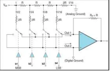
To overcome huge range of resistor used in weighted resistor D/A converter, R-2R ladder D/Converter is introduced. In this paper a 4-bit R-2R ladder resistor DAC is implemented.
The basic theory of the R-2R ladder network is that current flowing through any input resistor (2R) encounters two possible paths at the far end. The total resistances of both paths are the same (also 2R), so the incoming current splits equally along both paths. The half-current that flows back towards lower orders of magnitude does not reach the op amp, and therefore has no effect on the output voltage. The half that takes the path towards the op amp along the ladder can affect the output. The inverting input of the op-amp is at virtual earth. Current flowing in the elements of the ladder network is therefore unaffected by switch positions. The output voltage equation of DAC is given by
V0 = VR*(RF/R)[b1/21+ b2/22+ b3/23+ b4/24]
IJEDR1601074
International Journal of Engineering Development and Research (www.ijedr.org)454
A.OP-AMP
The OP-AMP implemented in this paper is a two stage OP-AMP to get high gain.
Fig 3: A two-stage OP-AMP
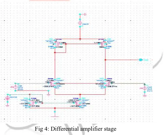
The first stage of OP-AMP consist of differential amplifier with current mirror is used to yield high gain, this stage rejects common mode signals like noise and amplifies differential signal.
Fig 4: Differential amplifier stage
IJEDR1601074
International Journal of Engineering Development and Research (www.ijedr.org)455
Fig 5: CS amplifierIII DESIGN OF R-2R LADDER RESISTOR DAC
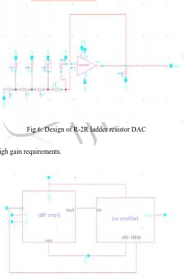
Design of R-2R ladder resistor DAC starts with two stage OP-AMP. So, Op-amp with power consumption in the order of few microwatts is to be designed. Beginning with this given power, and using supply voltage of 1.8V in 180nm n-well CMOS technology, value of total current flowing through the op-amp is calculated. Input transistors are designed so that maximum current flows through them, as the input transistors decide the gain of op-amp. Since, digital to analog converter is designed for 4-bit resolution; hence, minimum op-amp gain required is given by 2N+1 i.e. 42dB and phase margin greater than 600 for system to be stable.
. Fig 6: Design of R-2R ladder resistor DAC
A Design of OP-AMP
The op-amp is designed to meet high gain requirements.
IJEDR1601074
International Journal of Engineering Development and Research (www.ijedr.org)456
Equations
From slew rate and capacitance we can find current flowing through transistor
………..(1)
As M1 and M2are in saturation region using equation Vds>Vgs-Vt, as Vt=0.4v The current equation in saturation region is 2………...…(2)
2………..(3)
………...(4)
Gain bandwidth = ………..(5)
…..………..(6)
For calculating (W/L) ratio of M3 &M4 eq. (1&2) will used. M1 & M2 eq.(3,4,5,6) will used and for M5,M6 eq.3 will used.
IV SIMULATION RESULTS
Differential amplifier results
IJEDR1601074
International Journal of Engineering Development and Research (www.ijedr.org)457
Op-amp results
R-2R ladder resistor DAC results
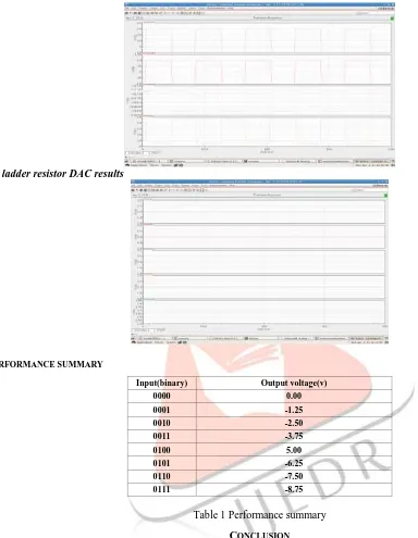
VPERFORMANCE SUMMARY
Input(binary) Output voltage(v)
0000 0.00
0001 -1.25
0010 -2.50
0011 -3.75
0100 5.00
0101 -6.25
0110 -7.50
0111 -8.75
Table 1 Performance summary
CONCLUSION
In this paper R-2R ladder resistor DAC is implemented and investigated .The DAC is designed to verify the characteristics. A DAC with two stages OP-AMP is designed to get high gain. The designed DAC is simulated using CADENCE 180nm technology with a gain of 50dB is achieved. Power dissipation is achieved by 480µw.
FUTURE WORK
In this paper 4-bit R-2R DAC is designed, this can be increased further and power dissipation can also be reduced.
ACKNOWLEDMENTS
I would like to thank the team of Siddhartha Institute of Technology & sciences for the facilities provided and consistent encouragement.
REFERENCES
[1] Ankit Upadhyay, Rajanikant M. Soni,3-bit R-2R Digital to Analog Converter with Better INL&DNL, IJEA,T ISSN: 2249 – 8958, Volume-2, Issue-3, February 2013
[2] P. E. Allen and D. R. Holberg, CMOS Analog Circuit Design, 2nd edition, Oxford University Press, 2002.pp.270-280,453-454..
IJEDR1601074
International Journal of Engineering Development and Research (www.ijedr.org)458
[3] Brandon Greenley, Raymond Veith, Dong-Young Chang, and Un-Ku Moon, A Low- Voltage 10-Bit CMOS DAC in 0.01-mm2 Die Area,IEEE TRANSACTIONS ON CIRCUIT AND SYSTEMS—II: EXPRESS BRIEFS, VOL. 52, NO. 5, MAY 2005M. Young, The Technical Writer’s Handbook. Mill Valley, CA: University Science, 1989.
[4] Brandon Greenley, Raymond Veith, Dong-Young Chang, and Un-Ku Moon, A Low- Voltage 10-Bit CMOS DAC in 0.01-mm2 Die Area, IEEE TRANSACTIONS ON CIRCUIT AND SYSTEMS—II: EXPRESS BRIEFS, VOL. 52, NO. 5, MAY 2005M. Young, The Technical Writer’s Handbook. Mill Valley, CA: University Science, 1989.
[5] Raghavendra. R, S. A Hariprasad, M. Uttara Kumari, Study of R2R 4-Bit and 8-Bit DAC Circuit using Multisim Technology, International Journal of Science and Research (IJSR),India Online ISSN:2319-7064 Volume 2 Issue 5, May 2013