2D Disturbance Map of Low-Power Front-End Circuits in Low
Frequency Band
Grzegorz Oleszek*
Abstract—This document presents an evaluation of a near-field contactless inductive link, examined from a radiated disturbance standpoint, whose sources are low-power Analog Front End (AFE) circuits. Two basic types of AFE rectifiers based on Shottky diodes and Mosfet transistors were tested. Due to selective interference measurement, a map of distortions regarding the position of the coil was created. The obtained results referred to the analytical model, providing sufficient convergence to quickly assess the optimum position of the receiving coil.
1. INTRODUCTION
Contactless interface based on near-field inductive links has numerous applications. One such example is Radio Frequency Identification (RFID) systems, which are used in access control, logistics, and animal marking. They are the basis of immobilizer systems [1] in the automotive industry, enabling two-way communication with the proximity key. In the case of basic configuration, such an interface consists of a transmitting coil and appropriately linked receiving coil, which is usually loaded with the active structure of Analog Front End (AFE) input circuit [2, 3]. Due to the variable orientation of coils and the non-linear nature of AFE circuits, optimal adaptation to the receiving coil (e.g., in the sense of the RF emission level) is usually possible only in a limited scope.
The above-mentioned systems usually operate in the 100 kHz..1.7 MHz frequency range, thus covering the generally available LF band (LW, MW). Therefore, ensuring compliance with the requirements of Electromagnetic Compatibility (EMC) becomes an additional key requirement that must be met by the entire interface.
This article presents evaluation results of the level of disturbances radiated in the LF band by two selected types of AFE, in reference to the position of the receiving coil. The first circuit aligns with the structure of a full-wave rectifier based on Shottky diodes. It demonstrates solutions used in basic RFID systems, such as those supplied with energy from the RF field [4–6]. The second circuit uses a rectifier based on Mosfet transistors and is additionally equipped with input-clipping circuits, whose purpose is to protect against elevated input voltage, including Electrostatic Discharge (ESD). Both of the analyzed AFE circuits were constructed from discrete components, which allowed for determination of the elementary input characteristics.
The main purpose of the research described in this article is the attempt to identify the correlations between the level of disturbances, introduced by a typical AFE, and the position of the receiving coil. The existence of this type of disturbance has been confirmed by Vera et al. [7, 8] but without reference to the position of coil connected to AFE. Despite the significance of such a relation, the available studies [4–6] presented it as unknown, or they only focused on the direct measurement of nonlinear AFE input impedance. In the work of [9], the harmonic disturbances were measured directly from the AFE time response, but without its reference to the emission level or the location in relation to the
Received 11 February 2019, Accepted 15 April 2019, Scheduled 25 April 2019 * Corresponding author: Grzegorz Oleszek ([email protected]).
transmitting antenna. Knowledge about this type of relation seems to significantly support the scope of estimation of the optimal position of the coils during the stage of system design, and it is a motivation behind this analysis.
This article is organized in the following manner. Section 2 includes a discussion on the principle of operation of the analyzed system. Section 3 demonstrates the details of its models, along with the achieved quality of mapping. Section 4 includes the circuit diagram and its components. Section 5 presents a measuring system in the ALSE chamber, as well as the measurement results that ultimately form a two-dimensional disturbance map. The last section contains a discussion of achieved results, as well as directions for subsequent works.
2. OPERATION OF RECTIFIER CIRCUIT
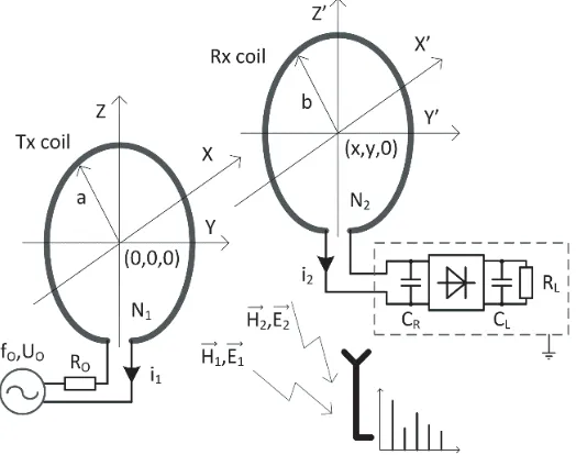
Figure 1 presents the analyzed circuit. The sinusoidal voltage generator with a low level of harmonic disturbances, operating at frequencyfO, output voltageUO, and output resistanceRO, controls the Tx transmitting coil. The Rx coil is located at (x, y,0) point, which has the capability to move. The mutual degree of the coils’ coupling, which is determined by mutual inductanceM and corresponding coupling factor k, results from the position of the receiving coil. An electric circuit consisting of capacitor CR and rectifier is connected to the Rx coil terminals, whose load consists of capacitorCL and resistorRL. The magnetic flux, which is generated by current i1, induces a voltage in the receiving coil that causes the flow of currenti2. Due to the nonlinear nature of the input impedance of the rectifier, currenti2, in addition to basic harmonicfO, also contains higher harmonics, 2fO, 3fO,. . ., which are treated in this analysis as disturbances. The magnetic fields,H1 andH2, and electric fields,E1 andE2 are summed up by the receiving antenna, placed in theY Z plane at a distance resulting from the accepted measurement standard [10]. The voltage generated in the antenna is subsequently measured by a spectrum analyzer, whose indications depend on the actual position (x, y) of the Rx coil; only for the simplification of the subsequent measurement was the immutability of dimension z assumed.
Figure 1. Analyzed circuit.
Both the frequencies and distances, at which the circuit is analyzed, allow us to assume the invariance of currents within the windings of each coil and the dominant inductive nature of the near field. Therefore, in accordance with [11], the total magnetic flux can be calculated
H·dL=N1i1(x, y) +N2i2(x, y) (1)
Further considerations focused on searching for the distorted forms of currents i1 and i2, which are dependent on the fixed position (x, y) as well as their reference to the measurements presented in Section 5. The analysis assumed a quasi-determined circuit state in which transient states of coil currents and capacitor voltages disappeared, while the only stimulation is the generator’s harmonic signal.
3. ANALYSIS OF CIRCUIT COMPONENTS 3.1. Inductive Coils
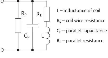
Serial components borrowed from a typical immobilizer application [1] and practically used in automotive vehicles were used as the Tx transmitting coil and Rx receiving coil. A parallel RLC structure (see Figure 2) was used to model them, which took into account the inter-winding capacity, finite resistance in the state of self-resonance, and losses associated with the resistance of windings [12].
Figure 2. Coil model.
Thus, the admittance of the substitute circuit, which describes the above-mentioned structure, can be expressed as
Y(ω) = 1
Rp
+ Rs
R2
s+ω2L2 +jω
Cp− L
R2
s+ω2L2
(2)
where
ω = 2πf0 (3)
Capacitance Cp and parallel resistance Rp were determined from the condition of self-resonance, i.e., Im{Y}= 0.
Cp = L
R2
s+ (2πfSRF)2L2
(4)
Rp =
1
1
Z(fSRF) −
Rs
R2
s+ (2πfSRF)2L2
(5)
Due to the proportions of used coils, i.e., (l+h)<2a, the nominal values of self-inductances were determined from the Wheeler’s equation for short coils [13]
L= aN 2
13.5log10
4.9a l+h
(6)
where the meaning of individual parameters is defined in Table 1.
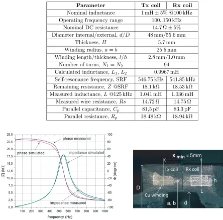
Measurement of amplitude-phase characteristics of Tx and Rx coils was carried out with the use of R&S ZVC vector analyzer in the 20 kHz–1 MHz band and supplemented by the measurement of winding resistance Rs. The measured characteristics of the exemplary coil Tx and its model are presented in Figure 3.
Table 1. Summary of coil reference and model data.
Parameter Tx coil Rx coil
Nominal inductance 1 mH±5% @100 kHz Operating frequency range 100..150 kHz
Nominal DC resistance 14.7 Ω±5% Diameter internal/external,d/D 48 mm/55.6 mm
Thickness,H 5.7 mm
Winding radius, a=b 25.5 mm
Winding length/thickness,l/h 2.8 mm/1.0 mm
Number of turns, N1 =N2 94
Calculated inductance,L1,L2 0.9967 mH Self-resonance frequency, SRF 546.75 kHz 541.85 kHz Remaining resistance, Z @SRF 18.1 kΩ 18.53 kΩ Measured inductance, L@125 kHz 1.041 mH 1.036 mH
Measured wire resistance, Rs 14.72 Ω 14.75 Ω Parallel capacitance,Cp 81,5 pF 83.3 pF Parallel resistance, Rp 18.48 kΩ 18.94 kΩ
Figure 3. |Z|and phase of Tx coil. Figure 4. Cross-section of Tx and Rx coils at closest position.
3.2. Mutual Inductance M and Coupling Factor k
To determine the mutual inductance, the method presented by Soma et al. [14] and used by [2, 15, 16] in the analysis of the efficiency of inductive energy transfer was applied. The works of [17, 18] are its extension, introducing the possibility of a more precise analysis of multi-winding coils based on replacing the integral from Equation (6) with its development into the Taylor series.
In accordance with [14], the mutual inductance M of two magnetically coupled coils that are separated from each other by (x, y,0) can be determined as
Mxy = μ20ab
π
2π
0 cosβ
√
abLG
where
r ≡
4abL (a+bL)2+x2
(8)
bL ≡
b2+y2+ 2bycosφ (9)
β ≡ tan−1
y·sinφ b+y·cosφ
(10)
while G(r) is defined in the following manner
G(r)≡
2
r −r
K(r)−2
rE(r) (11)
whereK(r) andE(r) are complete elliptic integrals of the first and second type, respectively.
The mutual inductanceM is associated with the coupling factor kby formula (12) [16–19], which makes it possible to refer it to the inductance values of the Tx and Rx coils.
kxy = √Mxy
L1·L2
(12)
It should be noted that Equation (7) applies to single-winding coils; thus, it is necessary to normalize Eq. (12) in relation to the number of windingsN1 andN2. Moreover, dimensionxin Equation (8) refers to the distance between the coil centers, which is the case of real coils preventing the juxtaposition of the positionx= 0. The minimum valuex, resulting from the positioning of the windings inside the coil housing, was assumed for the analysis, as illustrated in Figure 4.
The current value of the coupling factor k was determined in the range x = (5...35) mm,
y= (0...25) mm, based on [16]
kxy =
1− Lshort(x, y)
Lopen(x, y)
(13)
where Lshort(x, y) is the inductance measured at the Tx coil terminals with closed Rx coil terminals, and Lopen(x, y) is the inductance measured at the Tx coil terminals with opened Rx coil terminals in each of the analyzed positions (x, y).
Due to similar dimensions of Tx and Rx coils, the redetermination of the valuek from the side of the Rx receiving coil was abandoned, therefore assuming the full symmetry of the circuit [19].
The measurements were carried out with the use of an RLC bridge of HP 4284A type, with a basic accuracy of 0.1%, at a frequency of 125 kHz and excitation of 1 V. Due to the single measurement of each value of Lshort and Lopen, the estimation of the measurement error k was based on the following equation:
Δk= ∂k
∂Lshort ·
ΔLshort+ ∂k
∂Lopen ·
ΔLopen (14)
i.e.,
Δk= |−1|
Lopen ·
1
2
1−Lshort
Lopen
ΔLshort+Lshort
L2 open
· 1
2
1−Lshort
Lopen
·ΔLopen (15)
and finally
Δk= ΔLshort
Lopen·2k
+Lshort
L2 open
·ΔLopen
2k (16)
Noting that Lopen ≈ Lshort and, thus, assuming similar absolute errors of the inductance measurement of ΔLopen ≈ ΔLshort, it can be assumed that the error of determining k value from Eq. (13) amounts to
Δk∼= 2·ΔL
L·2k =
ΔL
Formula (17) indicates that there is a significant increase in the error for decreasing values of
k, i.e., for the most distant positions (x, y). The position x = 35 mm, y = 25 mm was assumed as the measurement limit in which repeatable k values were obtained, despite its main determination by
Lshort(Lopen was almost constant).
For large k values (i.e., smallx and y values), the error associated with the positioning of the Rx coil became dominant. This results from the high steepness of Mxy in Eq. (7) in this area, thus, the significant changes occurring for the uncertainty of the Δxand Δydisplacement. Determination of this error based on Eq. (7) is equivalent to finding a solution to the following equation:
ΔMxy =
∂Mxy
∂x ·Δx
2 +
∂Mxy
∂y ·Δy
2
(18)
It is not necessary to search for the analytical form of Equation (18) because ΔMxy can be determined directly as the gradient value ∇M(x, y). In practical implementation, the uncertainty of determination of the Δx and Δy positions was estimated at ±0.15 mm with the resulting highest value ΔMxy as 0.017 mH at the (5, 0) point.
Figure 5. Indicated value ofkover XY plane, log scale.
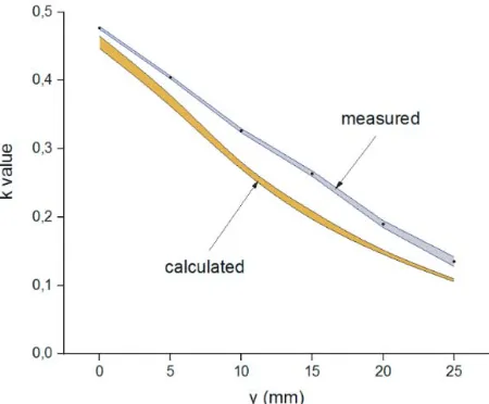
Figure 5 presents determined values kaccording to Eq. (13).
Figures 6 and 7 demonstrate the interdependence of Eqs. (12) and (13), taking into account the uncertainties in Eqs. (17) and (18). For the coaxial direction, i.e., along the X(5,0) → (35,0) axis, a precise mapping of the theoretical course is visible. For the transverse direction, i.e., along the
Y(5,0)→(5,25) axis, the impact of the coil thickness, which is not taken into account in Equation (6), is visible. The maximum deviation of such determined characteristics amounts to 0.052 at the (5, 15) point.
3.3. Rectifier Circuit
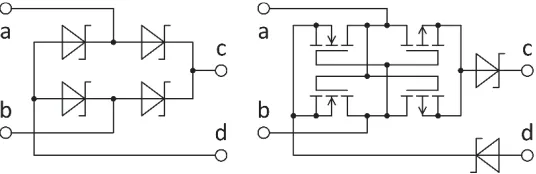
Figure 8 presents two analyzed AFE structures. The diode rectifier uses low-signal Shottky diodes of BAT54 type, characterized by the maximum conduction voltage amounting toVF = 0.32 V atIF = 1 mA and the capacitance of CD = 10 pF at VR = 1 V and f = 1 MHz. The transistor system is based on a configuration taken from [20], approximated with the use of a complementary pair of Mosfet low-power transistors of N3008N/PBK type, manufactured by Nexperia. This type was selected for its low switching voltageVGSth= 0.6 V(min) and internal clipping structure [20]. Two additional diodes on the rectifier output reflect solutions that eliminate the reverse leakage.
Figure 8. Analyzed AFE structures.
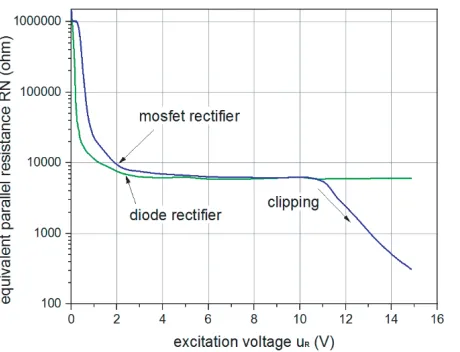
Due to the nonlinear nature of the AFE input, it was necessary to identify the real and imaginary parts of its input impedanceZN [4] as a function of the control voltageuR. During theZN measurement, the CR capacitor was disconnected from the input, assuming the constancy of its parameters in the analyzed frequency range and working voltages, which simultaneously removed its dominance in the analyzed circuit. It has also been noticed that, in the steady state, with constancy of fO, RL, and
CL, it is possible to simplify the analysis by replacing the four-terminal network by a two-terminal network — Figure 9, whose impedance is the only searched value. The nonlinear capacitive nature of two-terminal networks has been confirmed by subsequently implemented measurements of both AFE structures.
Figure 9. Rectifier simplification.
Figure 10. Resistance equivalentRN. Figure 11. Capacitance equivalentCN.
with low distortions and indirect determination of the input impedance from theS21 measurement was eliminated. The searched valuesRN,CN were directly obtained from the indications of the bridge with high accuracy. A similar solution was used in [12], yet only in a scope up to 2 V, resulting from the limitations of the used instrument. All measurements were controlled by an application based on the LabVIEW environment.
4. EQUIVALENT MODEL CIRCUIT
Figure 12 presents an electrical diagram consisting of components presented in Section 3. Its components include [21, 22]:
• source of sinusoidal voltage with frequency fO, output voltage UO, and internal resistance RO, representing the control generator;
• Tx transmitting coil with substitute parametersL1,RS1,CP1,RP1;
• mutual inductanceM, representing the current value of the coupling between the coils;
• Rx receiving coil, with substitute parameters L2,RS2,CP2,RP2;
• CR capacitor, which creates a resonance circuit with the receiving coil, which is single-point tuned to fO;
• reactance two-terminal networkRN,CN, representing the rectifier input.
The flows of i1 and i2 currents were numerically determined for interesting positions (x, y), by solving a system of nonlinear differential equations in the Mathcad environment. The distorted flows
obtained in this way were subjected to Fourier transform, which allowed the determination of the amplitudes and phases of the harmonics up to the 13th order.
5. RADIATION MEASUREMENT 5.1. RF Setup
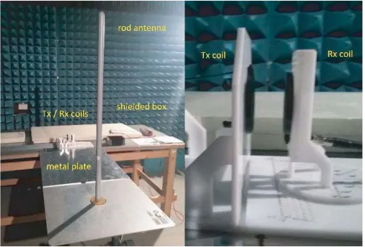
The measurements of electromagnetic emission were carried out in the ALSE chamber in accordance with the dedicated measurement setup, which is presented in Figure 13. It consisted of a non-magnetic base, on which a fixed Tx coil was placed at a height of 90 mm at a distance of 1 m from the measured antenna. The coil was controlled from the outside of the chamber by a Keysight 33220A generator, whose sinusoidal output signal was selected to obtain an emission level of approx. 74 dBµV/m, which corresponded to the voltage at the coil terminals 10.2Vpp. The value of this excitation was kept constant during all subsequent measurements, while the intensity of the obtained field referred to the maximum limit in the LW, MW [10] band, amounting to 72 dBµV/m for the RE310 emission. An additional margin was assumed as the uncertainty of the whole measuring path.
Figure 13. RF setup view.
After measuring the chamber’s background, the generator’s own disturbances were measured once by charging the Rx coil with a value close to |ZN|min, i.e., RL = 1 kΩ. During the measurement, the rectifier circuit was omitted. Due to the introduced circuit detuning, the position of the maximum coupling (thus, the largest load) was experimentally determined by searching for the minimum voltage
Uo at the generator output, which was monitored with the use of an oscilloscope. It was found that a generator with such a load did not introduce significant harmonic disturbances (<−65 dBc) or deviated from the limit declared by the manufacturer — Figure 14. At the initial stage, the disturbances of both tested circuits were also measured with the use of PK + AV detectors, confirming the convergence of their indications for periodic signals. The subsequent measurements were carried out only with the use of a PK detector with a measurement time of 50 ms.
The Rx receiving coil was placed on a handle with the possibility of adjusting the position in the direction of theXandY axes with a step of 1 mm and rotation every 5◦. The aluminum housing in which the coil load was placed (i.e., CR, rectifier, CL,RL) and the double-wire shielded cable that connected the receiving coil were grounded to a metal tabletop to minimize common disturbances coming from the distorted waveform at the rectifier output [23, 24].
RF emission was measured in the 100 kHz–1.7 MHz band in each of the positions of the Rx receiving coil. The measurements were carried out with a step of 5 mm in the range of x = (5...55) mm and
y = (0...15/20) mm. During all measurements, the load of each type of rectifier, i.e., CL = 8.3µF and
Figure 14. Tx signal quality @1 kΩ load. Figure 15. Emission spectrum of Mosfet rectifier, position (5, 0).
5.2. EMC Results
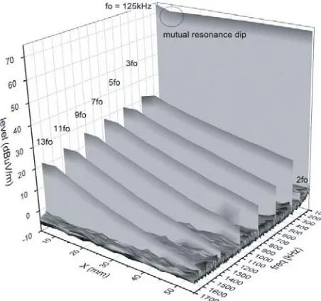
Figure 15 presents an example of the emission. The results collected in this manner were grouped depending on the type of rectifier and the direction ofX and Y displacement. Moreover, the values of selected harmonics, i.e., 2fo, 3fo...13fo, were separated and placed on a common diagram in order to observe the nature of the changes. In the form of supplementation, the place of the strongest coupling was located for the basic harmonic fo = 125 kHz (i.e., the largest decrease in the basic harmonic amplitude), whose presence was observed during the measurements of Mosfet-based rectifier.
6. DISCUSSION
Figure 16 presents the levels of disturbances registered for the diode rectifier along the X axis. There is a clearly visible strong dominance of the odd harmonics 3fO, 5fO..., which fade monotonically along with the increase in distance between the coils, wherein the quicker fading of the higher order harmonics is characteristic.
Figure 18 presents changes of disturbances in the transverse direction, i.e., along theY axis. In the scope of displacements, which are smaller than half of the coil radius, the levels of harmonics remained fairly uniform, with a maximum drop of −2 dBµV/m. Even harmonics 4fO, 6fO... from the response of the diode rectifier remained within the noise, not having a significant contribution into the analyzed spectrum. However, the relatively constant value of 2fOabove the background level is interesting, which suggests its origin directly from the generator; however, this is not observed in Figure 14. Alternatively, its source may be directly the waveform at the rectifier output and its incomplete shielding through the metal housing.
Figure 17 demonstrates changes of disturbance levels in the direction of theX axis for the rectifier with Mosfet transistors. For the maximal approximation of the coils, the increase in the value of all harmonics is clearly visible, which indicates the reduction of uR voltage by the internal clipping structures. This is also visible in Figure 15, where the acceptable limit value for the exemplary standard [10] is marked. In the range of x = 30...50 mm, there was a significant increase in even harmonics, despite the coils moving away from each other. This results from the squared characteristics
id=f(uR) in the area ofuR=±1 V, and it starts to dominate until the coupling fades away.
Figure 16. Radiation map of diode rectifier, directionX,y= 0 mm.
Figure 17. Radiation map of Mosfet rectifier, directionX,y= 0 mm.
Figure 18. Radiation map of diode rectifier, directionY,x= 10 mm.
Figure 19. Radiation map of Mosfet rectifier, directionY,x= 10 mm.
relative constancy of the level of radiated disturbances. The local maximum of coupling occurring in this region is manifested by the increase in disturbances, resulting from the flow of the higher current through the load and, therefore, through the rectifier. The position of this maximum can be located in (10, 5) by analyzing the change in the basic harmonic amplitude, as can be clearly seen in Figures 20 and 21.
Figure 20. Mutual resonance dip, Mosfet rectifier, fo= 125 kHz.
Figure 21. Mutual resonance dip, Mosfet rectifier, fo= 125 kHz, flat view.
The general accuracy is also affected by a significant simplification of the analysis, which does not take into account the position of the coils in relation to the monitoring antenna in an analytical manner [25, 26]. Considering the results summarized in Table 2, the convergence of disturbance mapping can be assumed to be approx.−35 dBc, which is a good result regarding the implemented simplifications. According to the opinion of the author, the main purpose of this analysis, i.e., the determination of the nature of disturbances depending on the current location of the coils, has been achieved.
Table 2. Summary of coil reference and model data.
spur N fO 2fO 3fO 4fO 5fO 6fO 7fO calculated 69.8 29.4 44.5 29.6 41.6 29.6 38.72
measured 73.3 31.8 45.9 21.2 38.4 5.60 33.2 spur N 8fO 9fO 10fO 11fO 12fO 13fO dBµ
V/m calculated 29.7 34.3 29.8 31.5 29.7 30.7
measured 7.59 31.2 2.94 29.1 4.52 27.1
7. CONCLUSIONS
Based on the theory of inductively coupled coils, the currents affecting the levels of disturbances radiated in the LF band were determined analytically in this article. They were determined in a variable range, resulting from the mutual position of the coils, limited only by their radii. The areas affecting a significant increase in emission levels, which are the local maxima of coupling and activation areas of clipping systems, were also identified. Moreover, the nature of even harmonic sources, which are the squared characteristics of Mosfet transistors, were confirmed. Another significant conclusion is the possibility of exceeding the emission limit by weakly coupled circuits, which may be overlooked in the scope of practical solutions.
REFERENCES
1. Knebelkamp, M. and H. Meier, “Latest generation technology for immobiliser systems,” Elektron, 2005.
2. Schormans, M., V. Valente, and A. Demosthenous, “Practical inductive link design for biomedical wireless power transfer: A tutorial,” IEEE Transactions on Biomedical Circuits and Systems, Vol. 12, No. 5, 1112–1130, 2018.
3. Cortes, F. P., J. P. M. Brito, R. Cantalice, E. Ghignatti, A. Olmos, F. Chavez, and M. Lubaszewski, “A low power RF/analog front end architecture for LF passive RFID tags with dynamic power sensing,”IEEE International Conference on RFID, 60–66, 2014.
4. Gvozdenovic, N., L. W. Mayer, and C. F. Mecklenbrauker, “Measurement of harmonic distortions and impedance of HF RFID chips,” The 8th European Conference on Antennas and Propagation (EuCAP 2014), 2940–2944, 2014.
5. Partal, H. P., A. T. Ince, M. A. Belen, S. Zorlu-Partal, and R. Tanski, “Electromagnetic modeling and analysis of rectifier antenas,” International Conference on Electromagnetics in Advanced Applications (ICEAA), 1489–1492, 2015.
6. Gvozdenovic, N., R. Prestros, and C. Mecklenbrauker, “HF RFID spiral inductor synthesis and optimization,” International Symposium on Wireless Personal Multimedia Communications
(WPMC), 53–59, 2014.
7. Vera, G. A., Y. Duroc, and S. Tedjini, “Redundant backscattering modulation of passive UHF RFID tags,” IEEE MTT-S International Microwave Symposium Digest, 1–3, 2013.
8. Vera, G. A., Y. Duroc, and S. Tedjini, “RFID air interface setup for power spectral density analysis,”
IEEE International Conference on RFID-Technologies and Applications, 193–197, 2012.
9. Vera, G. A., Y. Duroc, and S. Tedjini, “RFID test platform: Nonlinear characterization,” IEEE Transactions on Instrumentation and Measurement, Vol. 63, No. 9, 2299–2305, 2014.
10. JLR-EMC-CS v1.0 Amendment 4, “Electromagnetic
compatibil-ity specification for electrical/electronic components and subsystems,” http://www.jaguarlandrover.com/emc/docs/requirements.htm, 2015.
11. Kim, H., S. Jeong, D. H. Kim, J. Kim, Y. Kim, and I.-M. Kim, “Selective harmonic elimination method of radiation noise from automotive wireless power transfer system using active rectifier,”
IEEE 25th Conference on Electrical Performance Of Electronic Packaging And Systems (EPEPS), 161–164, 2016.
12. Gebhart, M., J. Bruckbauer, and M. Gossar, “Chip impedance characterization for contactless proximity personal cards,” 7th International Symposium on Communication Systems, Networks &
Digital Signal Processing (CSNDSP 2010), 826–830, 2010.
13. Wheeler, H. A., “Discussion on simple inductance formulas for radio coils,” Proceedings of the Institute of Radio Engineers, IEEE Journals & Magazines, Vol. 17, No. 3, 580–582, 1929.
14. Soma, M., D. C. Galbraith, and R. L. White, “Radio-frequency coils in implantable devices: Misalignment analysis and design procedure,” IEEE Transactions on Biomedical Engineering, Vol. 34, No. 4, 276–282, 1987.
15. Fotopoulou, K. and B. Flynn, “Optimum antenna coil structure for inductive powering of passive RFID tags,” IEEE International Conference on RFID, 71–77, 2007.
16. Duarte, R. M. and G. M. Felic, “Analysis of the coupling coefficient in inductive energy transfer systems,”Active and Passive Electronic Components, Vol. 2014, 2014.
17. Babic, S. I., J. Martinez, C. Akyel, and B. Babic, “Mutual inductance calculation between misalignment coils for wireless power transfer of energy,” Progress In Electromagnetics Research M, Vol. 38, 91–102, 2014.
18. Khan, S. R., S. K. Pavuluri, and M. P. Y. Desmulliez, “Accurate modeling of coil inductance for near-field wireless power transfer,” IEEE Transactions on Microwave Theory and Techniques, Vol. 66, No. 9, 4158–4169, 2018.
Conference (PEMC), 986–992, 2016.
20. Bakhtiar, A. S., M. S. Lajali, and S. Mirabbasi, “A high-efficiency CMOS rectifier for low-power RFID tags,” IEEE International Conference on RFID, 83–88, 2010.
21. Beams, D. M. and S. G. Annam, “Validation of a reflected-impedance design method for wireless power transfer applications,”IEEE 55th International Midwest Symposium on Circuits and Systems
(MWSCAS), 758–761, 2012.
22. Yang, M., Y. Wang, X. Zhang, and J. Li, “Analysis of reflected load model for inductively coupled power transfer systems,” Asia-Pacific Power and Energy Engineering Conference, 1–4, 2010. 23. Orlandi, A. and R. Scheich, “EMC in power electronic devices: Radiated emissions from a silicon
controlled rectifier,” Proceedings of IEEE Symposium on Electromagnetic Compatibility, 303–307, 1994.
24. Wunsch, B., U. Drofenik, S. Skibin, and V. Forsstrom, “Impact of diode-rectifier on EMC-noise propagation and filter design in AC-fed motor drives,” IEEE International Symposium on Electromagnetic Compatibility &Signal/Power Integrity (EMCSI), 237–242, 2017.
25. Reddy, V. S. and P. Kralicek, “Prediction of radiated emission pattern for the device under test,”
IEEE International Symposium on Electromagnetic Compatibility and 2018 IEEE Asia-Pacific
Symposium on Electromagnetic Compatibility (EMC/APEMC), 489–490, 2018.