Design of Flexible Passive Antenna Array on Kapton Substrate
Yvon G. Rabobason1, *, Greg P. Rigas2, 3, Srijittra Swaisaenyakorn4, Bobur Mirkhaydarov2, Blaise Ravelo1, Maxim Shkunov2,
Paul R. Young4, and Nabil Benjelloun1
Abstract—Recently, the RF/microwave electronic technology evolved with the consideration of plastic and organic substrates. Such a technology offers two-folded benefits: in one side for lowering the fabrication cost and in another side for the possibility to bend electronic devices. Such a technology is particularly interesting for the implementation of antenna system. This paper is dealing with the design of flexible microstrip 1×2 antenna array. Theoretical approach on the typically symmetrical 1×2 antenna array is proposed. The design methodology of microstrip antenna combined with 1 : 2 T-power divider (T-PWD) is described. Based on the transmission line theory, the S-parameter model of the antenna system with non-standard reference load is established. Then, the microstrip antenna passive system is theoretical analysed in function of the physical dimensions of the designed structure. The feasibility of the flexible antenna passive system is investigated with the proof-of-concept (POC) designed on Kapton substrate. The POC prototype consisted of microstrip 1×2 antenna array is designed to operate at about 5.8 GHz. Comparisons between the full wave simulated and measured return losses were performed. Then, simulated radiation pattern highlights the efficiency of the fabricated prototype of passive antenna array.
1. INTRODUCTION
The modern civilian and industrial automated environments require more and more wireless communication systems [1]. To meet the public and industrial demands, the wireless communication as the RFID and wearable devices evolves with constantly improved design techniques [2, 3]. In this way, a recent green and organic inkjet technology was emerged to meet challenging ecological and lowered cost [4–6]. Thanks to the challenging performances in terms of cost and outstanding compactness, the electronic flexible technology was recently adopted in the various fields of applications as RFID, WLAN technology and medical engineering [7–9].
The flexible RF/microwave circuit and antenna design is currently developed and promisingly advantageous in terms of costs. Therefore, the flexible antenna design topic attracts the attention of design and research engineers [10–13]. Accordingly, single planar designs of flexible bowtie antenna [10], dual-band antenna for WLAN applications [11], dual-band LCP antenna for RFID applications [12] and flexible monopole antenna [13] were recently performed. But the flexible antenna can be also imagined to be implemented on innovative systems as curved radar cross sections [14]. The radar front-end systems, for example, with electronic beam steering controls are usually implemented with antenna array [15, 16]. However, so far, little or no research work was carried out on the feasibility of antenna array system implemented in flexible or plastic technology. For this reason, the present research work
Received 9 December 2015, Accepted 20 March 2016, Scheduled 27 April 2016 * Corresponding author: Yvon Georges Rabobason ([email protected]).
is focused on the feasibility of simple 1×2 antenna array design methodology. To do this, the simple antenna topology is elaborated in microstrip technology [17].
Thanks to its potential of compactness, the microstrip antenna remains one of the most popular wireless terminal technologies [18–23]. In addition, the microstrip antenna theory can be exploited for the improvement of design technique [17–19]. However, the existing research work on the microstrip antenna is generally based on the classical rigid printed substrate [16–23]. As examples of research work available on this topic, one can cite the analysis of circular microstrip antenna [18], the influence on the antenna bandwidth [19, 20], the antenna E-shape topology [21], polarization circuit improvement [22] and even the investigation between the antenna and microstrip line [23]. Beyond the single antenna performance, the microstrip antenna array configuration enables to achieve higher performances in the matter of gain and the beam wave radiation. Moreover, the antenna arrays offer naturally significant degree of freedom to control the radiation pattern. In this paper, we are proposing the feasibility investigation on the design and implementation of typically passive antenna array as can be used in phased-array radar system [15, 16] in flexible technology. The investigation is based on the commercially available HN type Kapton substrate [24]. In addition to the flexibility aspect for the implementation of bended circuit, the choice of this substrate can be technically justified by the availability on its electrical and electromagnetic (EM) properties as the values of dielectric constant εr and loss tangent
tan(δ) which are noticeably interesting to achieve a significant antenna performance.
For the better understanding, the paper is essentially organized in three sections. Section 2 is dedicated to the design methodology of the proposed passive antenna array system. The study illustrates the choice of the Kapton HN type substrate and the synthesis method. In addition, the proposed 1×2 antenna array built with the T-tree power divider (T-PWD) as introduced in [25] will be modeled in non-standard reference loadS-parameter. This analytical approach is established from the transmission line theory in which physical dimensions and input impedances are studied. Section 3 described the proof-of-concepts (POCs) as the demonstrator prototype. The feasibility of the proposed antenna array design will be carried with comparisons between the full wave simulations and measurements of return losses. Finally, Section 4 is the paper conclusion.
2. DESIGN METHODOLOGY OF T-PWD BASED PASSIVE 1×2 ANTENNA ARRAY
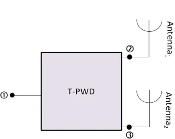
The proposed hexapole system constituted by single input and double output ports is composed of a 1 : 2 T-PWD terminated by microstrip antennas. The present section develops the design methodology of the antenna array topology and the S-parameter modelling. Then, the synthesis method of the antenna array is performed in function of the given return loss level.
2.1. Antenna Synthesis Method
The configuration of the microstrip antenna structure is depicted in Fig. 1. The microstrip antenna is assumed to be printed on dielectric substrate presenting thickness h and relative permittivity εr. The dielectric substrate is supposed with dimensionswsub×Lsub. The metallic conductor of the structure
is considered presenting thickness t, physical length dand widthw.
According to the transmission line (TL) theory, half-wave antenna dimension must present physical length din function of the resonance and radiating frequency f0 given by:
d=λg/2 =c/2f0√εeff
, (1)
with c the vacuum light speed and εeff the effective relative permittivity. Based on the Hammerstad and Jensen microstrip TL theory [26], the patch physical widthwcan be approximately determined by:
w=c/
f0
2(εr+ 1)
. (2)
(a) (b)
Figure 1. (a) Top and (b) side views of the considered microstrip antenna.
2.2. T-PWD Synthesis Method for the Antenna Array Design
As aforementioned, the 1×2 antenna array structure is designed with PWD configure in symmetrical T-tree. The electrical interconnections are constituted by microstrip lines with physical length to be determined later.
2.2.1. Configuration of the 1 : 2 Antenna Array System
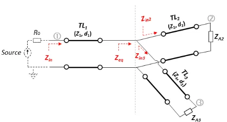
Similar to the topology proposed in [25], the symmetrical T-PWD under study is implemented in microstrip technology. Fig. 2 represents the 2D configuration of this typically single input and multiple outputs (SIMO) microstrip structure. It is noteworthy that in difference with the investigation developed in [25], this 1 : 2 tree distribution network is terminated with the microstrip antennas. The overall structure is printed on the flexible Kapton substrate. Furthermore, the T-PWD system input and output impedances are respectively denoted byR0 = 50 Ω and ZA which should be optimized in order to match the system input access.
This microstrip T-PWD is typically a hexapole topology with single input and double output. The illustrative diagram of the equivalent circuits can be found in Fig. 3. The overall system input port is denoted 1 and the output ports are denoted by 2 and 3. It can be emphasized that this T-PWD is loaded by the antenna input impedancesZA.2 and ZA.3. In other words, it acts as SIMO topology with input load R0 and outputs loads ZA.2 and ZA.3. The input interconnect line is represented by TL1(Z1, d1) which corresponds to a microstrip line with characteristic impedanceZ1 and physical lengthd1. Acting
Figure 2. 2D configuration of the proposed symmetrical T-PWD structure constituting the phased-array antenna system.
as a symmetrical T-tree, the interconnect lines TL2 and TL3 were assumed with the same dimensions w2 = w3 = w and d2 = d3 = d. In addition, the output loads corresponding to the antenna input impedances are also considered as identical ZA..2 =ZA..3 =ZA.
2.2.2. Analytical Modelling of the T-PWD Structure
The whole system proposed in Fig. 3 can be reduced by the SISO (Single Input Single Output) equivalent circuit as highlighted in Fig. 4. The overall and intermediate circuit input impedances are respectively denotedZinandZeq. The circuit analysis can be performed based on the configuration of these cascaded TLs.
The principal objective of this synthesis is to find the correct dimensions (w,d) of each part of the T-PWD line in order to obtain a return loss as low as possible (S11 → 0). Accordingly, we start this analysis within the initial conditions such as S11 = 0 and the length of the input TL (TL1) is quarter wavelength d1 = λg/4 . To determine the dimensions (w, d) of the transmission lines TL1, TL2 and TL3, we should deal with the characteristic impedances of each line (Z1, Z2 and Z3). It is worth to remind that the TL2and TL3are similar as proposed early in this part. Therefore the input impedances at the entry of each line are equal,Zin2 =Zin3, and the expression on the equivalent input impedance Zeq present in Figs. 3(b) and 4 is:
Zeq=Zin2//Zin3 ⇒Zeq =Zin2/2. (3)
According to the TL theory, Zin2 can be expressed as follows:
Zin2 =Z2ZA
+Z2tanh(γd2) Z2+ZAtanh(γd2),
(4)
where γ = α +jβ is the propagation constant. In addition, across the medium having relative permittivity εr =εr+jεr, the attenuation and phase constants are written as:
α = 2π
λg
εr
2
⎛ ⎝
1 +
εr
εr
2
−1
⎞
⎠, (5)
β = 2π/λg, (6)
with d2 the physical length of the TL2, Z2 the characteristic impedances of TL2, ZA the impedance of the load, γ the propagation constant, α and β respectively the loss and propagation constants. As explicated earlier in (3) and (4), these quantities are expressed in function of the complex permittivity of the dielectric and the wavelength. The loss coefficient α is neglected in the present configuration. Thus, the propagation constant is adopted to be equal to the constant phase. The input impedance in (4) becomes:
Zin2 =Z2ZA
+jZ2tan(βd2) Z2+jZAtan(βd2).
(7)
Figure 4. SISO equivalent circuit of the system presented in Fig. 3.
Moreover, the T-PWD input impedance can be formulated using the same approach as for the intermediate input impedanceZin2. Consequently, the global input impedance is written as:
Zin=Z1Zeq
+jZ1tan(βd1) Z1+jZeqtan(βd1),
(8)
Asd1=λg/4 and β = 2π/λg, this input impedance can be transformed as:
Zin=Z12/Zeq. (9)
By replacing Zeq with its expression in (3) and Zin2 established in (7), the previous relation can be transformed as follows:
Zin= 2Z
2
1[Z2+jZAtan(βd2)] Z2[ZA+jZ2tan(βd2)] .
(10)
2.2.3. Synthesis of the Characteristic Impedances of Elementary Lines Constituting the Proposed Passive Antenna Array System
The proposed passive antenna array is aimed to operate as a transmitter terminal. The analysis of the global phased array system is organized with combination of the two previous theoretical approaches. For starting the synthesis, the input impedance of the microstrip antenna and the T-PWD must be initially determined. Fig. 5 displays the configuration of the equivalent system topology. It can be seen that it is composed of the T-PWD and two symmetrical patch antennas which represent the loads at the end of each tree.
In order to reach the expected matching levelS11, the considered system input impedance can be determined from the relation:
S11(ω0) =S11⇒Zin=R0
1−S11 1 +S11.
(11)
By replacingZin formulated previously in (11) by the ideal case of the input matchingS11= 0, the TL1 and TL2 characteristic impedances Z1 andZ2 can be determined as follows:
Z1 =
ZAR0/2
Z2 =ZA . (12)
It can be pointed out from these expressions that these characteristic impedances do not depend on the physical length of the transmission lines TL2 and TL3. Meanwhile, the perfect matching condition of the T-PWD can be obtained independently to the constituting interconnect line physical lengths.
3. VALIDATION RESULTS
As aforementioned earlier, the aim of the present work is to verify practically the feasibility of the 1×2 antenna array design on the flexible substrate. After the description of the POC design on the Kapton substrate, the fabricated demonstrators will be explored. From the simulations and measurements of the demonstrators, discussions on the return losses and antenna gain enhancement compared to the single antenna will be performed.
3.1. Description of the Flexible Antenna Array under Study
After brief recall on the flexible Kapton substrate characteristics, the passive array microstrip antenna design was performed referring to the previous design synthesis methodology.
3.1.1. Kapton Substrate Description
is no known organic solvent, does not melt, does not burn and can be used in high or low temperatures. Adhesives are available for bonding the Kapton film on itself and to metals, on various types of paper or other layers. Depending on the application, there are three types of Kapton which are HN, VN and FN. For a behavioral (dielectric properties) and a thermomechanical stabilities criteria at the operating frequency 5.8 GHz, the HN type kapton better suite our study. The HN type Kapton acts as substrate layer all uses, while polyimide, successfully used for applications involving temperatures as low as −261◦C or rise to 400◦C [28]. The HN type can be laminated, metallized, punched, formed or coated with an adhesive layer. It is available with the commercialized samples having thickness 7.5µm, 12.5µm, 19µm, 25µm, 50µm, 75µm and 125µm. The 125µm thick kapton HN gives the better mechanical stability and will be considered for the rest of this article. As defined by the manufacturer datasheet [29], at the operating frequency 5.8 GHz, the Kapton relative permittivity presents dielectric constant εr= 3.35 and loss tangent tan(δ) = 0.007.
3.1.2. 2D Design of the POC Passive Antenna Array
The POC circuit was implemented on the Kapton substrate and the patches were synthesized to operate ideally at 5.8 GHz. This passive circuit was implemented in microstrip technology. Fig. 6 represents the 2D design of the fabricated demonstrator of passive 1×2 antenna array with the 3D simulation commercial tool HFSSRfrom AnsysR. The corresponding optimized physical parameters and the physical characteristic of the dielectric substrate are implemented in Table 1.
Figure 6. HFSS design of the tested passive 1×2 antenna array.
Table 1. Physical parameters of the POC phased 1×2 antenna array shown in Fig. 6.
Parameters Value
Wpatch 17.84 mm
Lpatch 13.79 mm
Wsub 92.26 mm
Lsub 51.3 mm
h(kapton dielectric thickness) 125µm
t (Cu metal conductor thickness) 17µm
W1 0.34 mm
W2 0.3 mm
d1 11.05 mm
3.2. Simulation and Experimental Validation Results
The validations of the POC presented in the previous paragraph were made numerically with EM full wave simulations by employing the commercial tool HFSSR. After comparisons between the simulated and experimented return losses of the global antenna system, the antenna radiation pattern will be explored and discussed in this subsection.
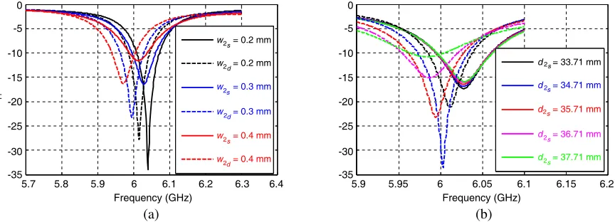
3.2.1. Analyses of Fabricated Prototype in Terms of Simulated and Measured Return Losses S11 Comparison between the return losses from single and double antenna structures were realized based on the HFSS full wave simulations. The obtained results by varying the physical width w2 = (300 +/−100)µm and the length d2 = (35.7 +/−2) mm are displayed respectively in Fig. 7(a) and Fig. 7(b).
(a) (b)
5.7 5.8 5.9 6 6.1 6.2 6.3 6.4
Frequency (GHz)
5.9 5.95 6 6.05 6.1 6.15 6.2
Frequency (GHz) 0 -5 -10 -15 -20 -25 -30 -35 S (dB) 11 0 -5 -10 -15 -20 -25 -30 -35
w = 0.2 mm
w = 0.2 mm
w = 0.3 mm
w = 0.3 mm
w = 0.4 mm
w = 0.4 mm 2 2 2 2 2 2 s d s d d s
d = 33.71 mm
d = 34.71 mm
d = 35.71 mm
d = 36.71 mm
d = 37.71 mm
2s
2s
2s
2s
2s
Figure 7. Comparisons between simulated return losses from single patch antenna and double antenna array with variation of physical parameters (a)w2 and (b)d2.
It can be emphasized that the double antenna structure return losses (here plotted in dashed line) with resonance frequency below 6 GHz is generally better for the physical widthw2 lower than 300µm. As can be understood in Fig. 7(b), the single antenna return losses are less affected by the considered variation ofd2. However, the matching level is decreased around the critical value d2 = 34.7 mm.
Before the implementation of the antenna array prototype, optimization process following the routine algorithm depicted in Fig. 8 was performed. The initial values ofZ1,Z2 andZAwere determined for the target level of the input return lossS11=−15 dB. Then, the T-PWD constituting TL physical widthsw1,w2 and wA were successively updated during the HFSS simulation of the overall structure. Then, the final values of the T-PWD physical parameters were considered for the prototype.
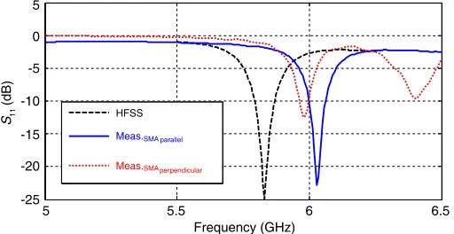
In order to investigate the practical influence of the antenna excitation feeding positions, two antenna array prototypes excited by parallel and perpendicular configurations of the feeding SMA connectors were fabricated and tested. The implemented two antenna arrays were realized in order to choose the most efficient one regarding the feeding connector configuration. The photographs of the passive antenna arrays are displayed in Fig. 9. The illustrative of the fabricated structure bending aspect along a circular cylinder can be understood with Fig. 10. These antenna prototypes were initially synthesized to operate at about 5.8 GHz.
Figure 8. Routine algorithm of the simulated circuit optimization.
(a) (b)
Figure 9. Photograph of the 1×2 antenna array demonstrators with SMA connector excitation in (a) perpendicular and (b) parallel configurations.
in account in simulation. Additionally, the frequency shift between simulations and measurements can be explained with the fabrication inaccuracies and also the dispersion of the Kapton substrate dielectric characteristics.
Figure 10. Photograph of the bended flexible 1×2 antenna array.
5 5.5 6 6.5
Frequency (GHz) 5
0
-5
-10
-15
-20
-25
S
(dB)
11 HFSS
Meas.
Meas.SMA
SMA
perpendicular
parallel
Figure 11. Simulated and measured return losses from the prototypes of passive antenna array for perpendicular (blue curve) and parallel (dotted red curve) SMAs.
parasitic radiation from the excitation point. The above phenomenon on return loss for the parallel SMA connector can be explained by the presence of parasitic waves from the feeding network. In this configuration, the parasitic waves are in phase with the incident field which can be added as loss power and lead to a fall of the accepted power. The feeding network resonance is responsible of second resonance frequency. It can be emphasized that it is better to consider a perpendicular SMA connector in order to reduce the parasitic power from the feeding network and maximize the accepted power. Therefore, this configuration is suggested for the simulation and measurement validations of the two array passive patch antenna. This effect illustrates the advantages offered by the microstrip antenna with perpendicular configuration excited from the ground plane.
3.2.2. Analyses and Validation of Measured and Simulated Radiation Patterns from the Simulated 1×2 Antenna Array
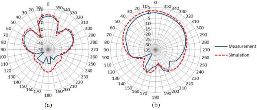
In order to validate the simulated radiation patterns, measurements were performed at the resonance frequency 6.02 GHz. The antenna prototype shape was held in planar configuration during the measurement process in an anechoic chamber. A comparison between measured and simulated radiation patterns in terms of realized gain is depicted in Fig. 12.
accuracy and measurement uncertainties, subsequently, the experimental results enable to validate the proposed antenna design concept.
Moreover, HFSS full wave simulations were performed for both planar and bended configuration of the array antenna in order to visualize the effects of bending the antenna. The simulated 2D radiation patterns over the realized gain of the 3D structure introduced in Fig. 6 are displayed in Fig. 13.
(a) (b)
Figure 12. Measured (solid lines) and simulated (dotted lines) radiation patterns in elevation planes for (a) Phi = 90◦ and (b) Phi = 0◦.
(a)
(b)
(d)
(c) (f)
Figure 13. Polar views of simulated radiation patterns in elevation plane in terms of realized gain on (a), (b), (c) respectively for planar, bending configurations 1 and 2 @ Phi = 90◦ and (d), (e), (f) respectively for planar, bending configurations 1 and 2 @ Phi = 90◦.
5 5.5 6 6.5
Frequency (GHz) 0.2
0.15
0.1
0.05
0
Radiation efficiency
Total efficiency
Efficiency
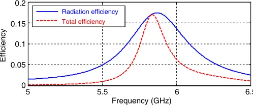
Figure 14. Simulated total and radiation efficiencies.
The radiation patterns atϕ= 90◦, show the maximum realized gains of 1.9 dB in the main direction
θ = 0◦ for the planar antenna, −0.61 dB at θ = 0◦ for the bended configuration 1 and −5.04 dB at
θ = 180◦ for the bended configuration 2. At ϕ = 0◦, the maximum magnitudes of realized gains are quite identical where for the planar antenna Gmax = 2.33 dB (θ = 14◦), bended configuration 1 Gmax=−0.31 dB (θ= 15◦) and for bended configuration 2Gmax=−4.53 dB (θ= 160◦).
From these results, especially for the cases whereϕ= 90◦, it can be underlined that the main lobe of radiation pattern for the bended configuration 2 is progressively switching to the opposite direction (θ= 180◦) compared to the radiation pattern at the planar state of the antenna. This is can be explained by the fact that the geometrical position of the 2 radiating elements of the antenna, in our case, is in the back side compared to the one in planar configuration. Moreover, the bended antennas are less directional than the planar first because the radiating elements are in this case physically close, which results in an increase of coupling between these elements, thus increase of destructive interferences. Secondly, in bending the antenna the ground plane is electrically small than in planar configuration therefore the reflecting effect of the ground plane is reduced which result is a decreased magnitude of the radiation pattern.
In the other side, the magnitude of the realized gain is decreasing when bending the antenna, a phenomena which joins the explanation above where the planar antenna has a more directive radiation pattern because there are less coupling between radiating elements and also the ground plane is electrically bigger.
4. CONCLUSION
A feasibility analysis and design of flexible microwave circuit consisted of the passive antenna array on the Kapton substrate is investigated. First, the analytical approach enabling to perform the design methodology is established. The antenna system comprised of microstrip antenna and T-PWD is elaborated based on the TL theory. Based on the T-structure SIMO/SISO transform of the array system, the equivalent input and output impedances were formulated in function of the interconnect line characteristics constituting the T-PWD. Then, the synthesis relation for calculating the optimal antenna input impedance is established.
After optimization, a POC of microstrip passive 1×2 antenna array printed on Kapton substrate was designed, simulated, fabricated and measured. A good correlation between the simulations and measurements of the return losses were found. Furthermore, the radiation pattern and efficiency from HFSS full wave simulations were analyzed. It was stated that the antenna gain can be increased with the array antenna compared to the single antenna.
The proposed flexible antenna system is beneficial in terms of the directivity thanks to the mechanical flexible of the substrate. Moreover, the developed antenna and PWD structure is very useful for the future generation of the RF/analogue wireless communication devices. For example, with the rising interests on the future technology as wearable and connected objects, the flexible antenna system is a promising solution for the RF/microwave designers. Among the most important applications, one can cite also the engine structures (automobile, aircraft. . ..) of communication terminals with arbitrary and irregular shapes. Finally, the flexible antenna on plastics is also expected as a good candidate to reduce the design cost.
REFERENCES
1. Lee, J.-S., C.-C. Chuang, and C.-C. Shen, “Applications of short-range wireless technologies to industrial automation: A ZigBee approach,” Proc. of 5th Advanced International Conference on Telecommunications, 2009 (AICT’09), 15–20, Venice, Italy, May 24–28, 2009.
2. Yang, L. and M. M. Tentzeris, “Design and characterization of novel paper-based inkjet-printed RFID and microwave structures for telecommunication and sensing applications,” Proc. of IEEE MTT-S International Microwave Symposium (IMS’07), 1633–1636, Honolulu, HI, Jun. 3–8, 2007. 3. Monti, G., L. Corchia, and L. Tarricone, “Fabrication techniques for wearable antennas,” Proc. of
European Radar Conference (EuRAD) 2013, 435–438, Nuremberg, Germany, Oct. 9–11, 2013. 4. Konstas, Z., A. Rida, R. Vyas, K. Katsibas, N. Uzunoglu, and M. M. Tentzeris, “A novel “Green”
inkjet-printed Z-shaped monopole antenna for RFID applications,” Proc. of IEEE 3rd European Conference on Antennas and Propagation (EuCAP’09), 2340–2343, Berlin, Germany, Mar. 23–27, 2009.
5. Main, Y., Q. Chen, L.-R. Zheng, and H. Tenhunen, “Development and analysis of flexible UHF RFID antennas for “Green” electronics,” Progress In Electromagnetics Research, Vol. 130, 1–15, 2012.
6. Yang, L., L. Martin, D. Staiculescu, C. P. Wong, and M. M. Tentzeris, “Design and development of compact conformal RFID antennas utilizing novel flexible magnetic composite materials for wearable RF and biomedical applications,” Proc. of Antennas and Propagation Society International Symposium 2008, 1–4, San Diego, CA, Jul. 5–11, 2008.
7. Kim, D. O., C. Y. Kim, and D. G. Yang, “Flexible Hilbert-curve loop antenna having a triple-band and omnidirectional pattern for WLAN/WiMAX applications,” Int. Journal Antenna and Propagation, Vol. 2012, 1–9, 2012.
8. Raad, H. R., A. I. Abbosh, H. M. Al-Rizzo, and D. G. Rucker, “Flexible and compact AMC based antenna for telemedicine applications,”IEEE Trans. on Ant. and Propag., Vol. 61, No. 2, 524–531, Feb. 2013.
10. Durgun, A. C., M. S. Reese, C. A. Balanis, C. R. Birtcher, D. R. Allee, and S. Venugopal, “Design, simulation, fabrication and testing of flexible bow-tie antennas,”IEEE Trans. on Ant. and Propag., Vol. 59, No. 12, 4425–4435, Dec. 2011.
11. Chien, H.-Y., C.-Y.-D. Sim, and C.-H. Lee, “Compact size dual-band antenna printed on flexible substrate for WLAN operation,”Proc. of Int. Symp. on Antennas and Propagation (ISAP), 2012, 1047–1050, Nagoya, Japan, Oct. 29–Nov. 2, 2012.
12. Paul, D. L., L. Zhang, and L. Zheng, “Flexible dual-band LCP antenna for RFID applications,” Proc. of URSI International Symposium on Electromagnetic Theory (EMTS) 2013, 973–976, Hiroshima, Japan, May 20–24, 2013.
13. Khaleel, H. R., H. M. Al-Rizzo, and A. I. Abbosh, “Design, fabrication, and testing of flexible antennas,” Intech Open Book, Advancement in Microstrip Antennas with Recent Applications, ed. by A. Kishk, Chap. 5, 363–383, Mar. 2013.
14. Knott, E. F., J. F. Shaeffer, and M. T. Tuley,Radar Cross Section, 2nd Edition, SciTech Publishing, Inc., Raleigh, NC, 2004.
15. Fenn, A. J., D. H. Temme, W. P. Delaney, and W. E. Courtney, “The development of phased-array radar technology,” Lincoln Laboratory Journal, Vol. 12, No. 2, 321–340, 2000.
16. Eldek, A. A., A. Z. Elsherbeni, and C. E. Smith, “Wideband 2D array of microstrip fed rectangular-slot antennas for radar applications,” Microwave and Optical Technology Letters, Vol. 46, No. 1, 36–40, Oct. 2005.
17. James, J. R., P. S. Hall, and C. Wood, Microstrip Antenna Theory and Design, 103–109, Peter Peregrinus, Ltd, New York, USA, 1981.
18. Verma, A. K. and Nasimuddin, “Analysis of circular microstrip antenna of thick susbstrate,” Journal of Microwaves, Optoelectronics, and Electromagnetics Applications, Vol. 2, No. 5, 30–38, Jul. 2002.
19. Kumar, G. and K. P. Ray, Broadband Microstrip Antennas, Artech House, 2002.
20. Goswami, K., A. Dubey, G. C. Tripathi, and B. Singh, “Design and analysis of rectangular microstrip antenna with PBG structure for enhancement of bandwidth,”Global Journal of Research Engineering, Vol. 11, No. 2, 22–28, Mar. 2011.
21. Ang, B.-K. and B.-K. Chung, “A wideband E-shaped microstrip patch antenna for 5–6 GHz wireless communications,”Progress In Electromagnetics Research, Vol. 75, 397–407, 2007.
22. Kasabegoudar, V. G. and K. J. Vinoy, “A broadband suspended microstrip antenna for circuit polarization,” Progress In Electromagnetics Research, Vol. 90, 353–368, 2009.
23. Ojha, J. R. and M. Peters, “Patch antennas and microstrip lines,” Intech Open Book, Microwave and Millimeter Wave Technologies: Modern UWB Antennas and Equipment, 50–62, Rijeka, Croatia, Mar. 2010.
24. Polyimides, UBE America Inc, http://www.ube.com/content.php?pageid=130, accessed 2015. 25. Ravelo, B., “Behavioral model of symmetrical multi-level T-tree interconnects,” Progress In
Electromagnetics Research B, Vol. 41, 23–50, 2011.
26. Hammerstad, E. and O. Jensen, “Accurate models for microstrip computer aided design,” IEEE MTT-S Int. Microwave Symposium Digest, 407–409, Washington, DC, May 28–30, 1980.
27. Balanis, C. A.,Antenna Theory: Analysis and Design, Chap. 6, 2nd Edition, Wiley, 1997. 28. Polyimides, UBE America Inc, http://www.ube.com/content.php?pageid=130, accessed 2015. 29. http://www2.dupont.com/Kapton/en US/assets/downloads/pdf/HN datasheet.pdf, accessed