ABSTRACT
KLEINERT, JAIRUS MATTHEW. Liquid Transport and Colloidal Self Assembly in Thin Wetting Films Driven by Electric Fields. (Under the direction of Dr. Orlin D. Velev).
Three systems in which electric fields are used to control the flow of liquid in thin
wetting films are presented. First, a new technique that combines evaporative convective
deposition of colloidal crystal coatings with an electric field to achieve more rapid assembly
and reduce the occurrence of defects in the crystal structure is reported. When an ac voltage
was applied across the particle suspension and the substrate in the convective assembly
process, a longer film spread from the meniscus by the electrowetting effect. The data
suggest that the electrowetting-increased liquid surface area resulted in increased
evaporation-driven particle flux and crystal assembly that was up to five times more rapid
than without voltage applied. The extended drying film also provided more time for particle
rearrangement before the structure became fixed, resulting in formation of crystal domains an
order of magnitude larger than those deposited by convective assembly alone. The results
demonstrate that electrowetting is a facile tool for controlling particle assembly processes in
wetting films. The technique could be used in improved large-scale colloidal crystal coating
processes.
Second, oil films that separate water droplets from solid surfaces in microfluidic
systems are examined during actuation of droplets using an electric field. The films are
critical to lubrication of droplet motion and prevention of fouling of the devices. The factors
microfluidic cartridge in which water droplets were enclosed in an oil-filled gap over an
array of electrodes. Programmable electrode switching sequences actuated two-dimensional
droplet motion driven by electrowetting. Stable, continuous oil films separated the droplets
from the surfaces when the droplets were stationary. During droplet transport, waves trailed
the receding oil meniscus in the film over the electrode-embedded surface. The waves
evolved into semispherical oil lenses. Droplet deformation and oil displacement caused the
film at the surface above the droplet to transform into a dimple of oil. Lower actuation
voltages were associated with slower film thinning and fewer but larger oil lenses. Lower ac
frequencies induced vibrations in the droplets that caused the films to rupture. Films were
also destabilized by addition of surfactants to the oil or droplets. The understanding of oil
film behavior provided by this work will enable more robust electrowetting-actuated
lab-on-a-chip devices through minimization of molecular transfer between droplets.
Finally, a novel nanofluidic system based on electroosmotic flow in nanoscale-thin
aqueous wetting films is described. The water films formed spontaneously on mica substrates
in a saturation humidity environment. The film thickness was determined to be a few tens of
nanometers by optical interference and fluorescence intensity measurements and was
consistent with a theoretical evaluation of the thickness of a film based on the competing
forces of electrostatic repulsion and capillary pressure. Lateral flow was induced by applying
a dc electric field tangential to the film and characterized by tracking the position of a
fluorescent probe. The mobilities of the thin fluid layer and the flow marker were lower than
the predictions of electrokinetic theory, which may be a result of adsorption of the
substrate. This system has the advantage of simple and inexpensive fabrication in comparison
Liquid Transport and Colloidal Self Assembly in Thin Wetting Films Driven by Electric Fields
by
Jairus Matthew Kleinert
A dissertation submitted to the Graduate Faculty of North Carolina State University
in partial fulfillment of the requirements for the degree of
Doctor of Philosophy
Chemical Engineering
Raleigh, North Carolina
2013
APPROVED BY:
________________________________ ________________________________
Orlin D. Velev Jan Genzer
Committee Chair
________________________________ ________________________________
Michael Dickey Glenn M. Walker
BIOGRAPHY
Jairus Kleinert was born on May 18, 1984 in Grand Rapids, Michigan to John and
Karen Kleinert, a chemical engineer and a teacher. He was raised in Livingston County,
Michigan with his sister Anna and brothers, Jonathan and Benjamin. While attending high
school near Charlotte, North Carolina, Jairus realized that his deepest interests were in the
fields of chemistry and biology. Upon enrolling as an undergraduate at Michigan State
University (MSU), he elected to major in chemical engineering, attracted to a curriculum that
emphasized using knowledge of the physical world to solve significant problems in practical
ways. Throughout his time at MSU, Jairus worked in the research lab of Professor Robert M.
Worden, developing novel biosensors and catalysts based on redox enzymes. After earning
his bachelor’s degree, he began graduate school at North Carolina State University, studying
colloid science under Professor Orlin D. Velev. With an interest in microfluidic devices,
Jairus performed some of his dissertation work at Advanced Liquid Logic (ALL), a newly
established, local company developing a lab-on-a-chip platform based on electrowetting.
Jairus has continued working at ALL and is now developing microfluidic assays that are
enabling expanded screening and early treatment of newborns for several potentially
ACKNOWLEDGMENTS
I am grateful to the many people who have contributed to my endeavors in graduate
school. From the beginning, my family has supported my education and encouraged my
aspirations. Significant sacrifices by parents and grandparents over the years have opened
critical opportunities to me.
Several excellent teachers have prepared me for graduate research. Recognition is
especially due to Tradd Medford, my high school chemistry and physics teacher, who
kindled my early interest in science, and Professor Worden, my undergraduate advisor, who
generously hired me when I knew very little and taught me what doing research really means.
The distinguished and collegial faculty and helpful staff at North Carolina State
University have contributed greatly to my learning. I have been especially influenced by
Professors Genzer, Walker, and Dickey, who have served on my committee, taught
interesting courses, and contributed professional advice. The support of Professor Kelly
through the Molecular Biotechnology Training Program has added a valuable dimension to
my expertise. Sandra Bailey has been indispensable in navigating the various university
departments and procedures.
My graduate research experience has been enriched by interactions with faculty and
colleagues and at other institutions as well. In the Department of Chemistry at the University
of North Carolina at Chapel Hill, Michael Barrett and Professor Sheiko engaged with us in a
stimulating collaboration on polymer flows. Abigail Turner, Jacob Grohman, and Professor
Allbritton provided valuable assistance with electrokinetic measurements. At Advanced
lithography and electrical engineering. Arnaud Rival and Cyril Delattre shared
complementary observations of droplet dynamics. Ramakrishna Sista and Theodore Winger
provided useful advice. Vijay Srinivasan welcomed me to the company and is a reservoir of
electrowetting knowledge.
Working with the talented assembly of researchers in the Velev Group has been a
privilege. The senior graduate students and postdocs—Brian Prevo, Ketan Bhatt, Daniel
Kuncicky, Shalini Gupta, Suk Tai Chang, Lindsey Jerrim, Vinayak Rastogi, Sumit Gangwal,
Bridgette Budhlall, Stoyan Smoukov, and Elena Blanco—have been role models of
uncommon intelligence, dedication, and kindness. I am especially grateful to Sejong Kim
who helped me to begin my experiments. The camaraderie among my contemporaries in the
group—Elizabeth Melvin, Hyung Jun Koo, Jessica Jenkins, Burak Uçar, Rachita Sharma,
Stephanie Lam, and Tian Tian—is deeply appreciated.
My friends at NCSU, Matthew Anderson, Christopher Bonino, Jeremy Palmer, Sara
Arvidson, Michelle Casper, Kristen Roskov, and Joshua McClure, have made the past six
years happy ones.
Finally, two excellent mentors have been chiefly responsible for my intellectual and
professional development during graduate school. Vamsee Pamula, who has overseen my
research at Advanced Liquid Logic, has motivated me with his passion and energy,
challenged me to think more quickly with his countless questions, and inspired me with his
commitment to improve the lives of other people. Above all, my advisor, Professor Velev has
creativity, and guided my work with graciousness and patience. He will always have my
TABLE OF CONTENTS
LIST OF TABLES ... viii
LIST OF FIGURES ... ix
Chapter 1: Introduction to Wetting Films, Electric Field Effects,
Microfluidics, and Colloidal Self Assembly ...1
1.1 Introduction ...1
1.2 Wetting Films ...2
1.2.1 Wetting Thermodynamics...2
1.2.2 Disjoining Pressure ...4
1.2.3 External Forces ...8
1.3 Electric Field Effects in Colloidal Systems ...9
1.3.1 Electrophoresis and Electroosmosis ...9
1.3.2 Dielectrophoresis ...11
1.3.3 Electrowetting ...12
1.4 Microfluidics ...15
1.4.1 Applications ...15
1.4.2 Physics of Microscale Flow ...18
1.4.3 Microfabrication ...21
1.4.4 Device Configurations ...23
1.4.5 Nanofluidics ...25
1.5 Colloidal Self-Assembly ...26
1.5.1 Applications ...26
1.5.2 Assembly Driven by External Fields ...29
1.5.3 Assembly Driven by Solvent Flow ...30
1.5.4 Assembly Driven by Molecular Interactions ...32
1.5.5 Assembly with Anisotropic Particles ...33
1.6 Overview of Dissertation ...34
1.7 References ...35
Chapter 2: Electric-Field-Assisted Convective Assembly of Colloidal
Crystal Coatings ...50
2.1 Introduction ...50
2.2 Materials and Methods ...51
2.2.1 Materials ...51
2.2.2 Coating Deposition ...52
2.2.3 Characterization of the Coatings ...54
2.3.2 Effect of Electric Field on Crystal Uniformity ...64
2.4 Conclusions ...69
2.5 References ...70
Chapter 3: The Dynamics and Stability of Lubricating Oil Films During
Droplet Transport by Electrowetting in Microfluidic Devices ...72
3.1 Introduction ...72
3.2 Materials and Methods ...77
3.2.1 Microfluidic Cartridge Construction ...77
3.2.2 Liquid Phase Materials ...79
3.2.3 Electrical Instrumentation ...79
3.2.4 Characterization ...80
3.3 Results ...81
3.3.1 Static Oil Films ...81
3.3.2 Oil Films Formed During Stationary-Droplet Electrowetting ...83
3.3.3 Dynamics of Oil Films During Electrowetting-Driven Droplet Transport ...84
3.3.4 Effects of Voltage Magnitude and Frequency ...88
3.3.5 Effects of Surfactants ...92
3.4 Discussion...94
3.5 Conclusions ...101
3.6 References ...102
Chapter 4: Electric-Field-Controlled Flow in Nanoscale-Thin Wetting
Films ...104
4.1 Introduction ...104
4.2 Materials and Methods ...105
4.2.1 Flow System Construction ...105
4.2.2 Characterization of Wetting Films and Flow Behavior ...109
4.3 Results ...110
4.3.1 Initial Demonstration of Wetting Film Formation and Flow ...110
4.3.2 Measurement of Film Thickness ...112
4.3.3 Measurement of Electroosmotic Mobility ...115
4.4 Discussion...120
4.5 Conclusions ...125
4.6 References ...126
Chapter 5: Summary and Outlook ...129
5.1 Summary ...129
5.2 Outlook...131
LIST OF TABLES
Table 3.1. Effect of voltage magnitude and frequency on droplet transport and oil
film evolution. ...89
Table 3.2. Effect of surfactant concentration on droplet-oil interfacial tension and
LIST OF FIGURES
Figure 1.1. Schematics of partial and complete wetting configurations of a liquid on a solid substrate and contributions to disjoining pressure that determine wetting film
thickness. ...3
Figure 1.2. Schematic depiction of the electric field effects that are operative in microscale systems...11
Figure 1.3. Composite of schematics and images of microfluidic devices. ...20
Figure 1.4. Images of colloidal assemblies. ...29
Figure 1.5. Schematic of convective assembly coating deposition process. ...32
Figure 1.6. Images of colloidal assemblies from anisotropic particles. ...34
Figure 2.1. Schematics of the apparatus used to deposit colloidal crystal coatings by convective assembly in an electric field. ...53
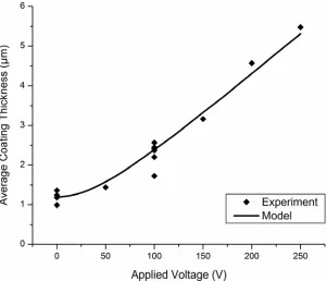
Figure 2.2. Plot of the average thicknesses of crystal coatings deposited with different voltages applied. ...58
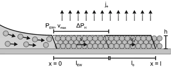
Figure 2.3. Schematic of the parameters for the model of voltage-driven extension of the particle suspension drying film. ...60
Figure 2.4. Images of crystal domains in coatings deposited with and without an electric field and optical micrograph showing individual particles in a crystal coating deposited without an electric field and the alignments of domains. ...65
Figure 2.5. Histogram comparing the sizes of crystal domains in coatings deposited with and without an electric field. ...67
Figure 2.6. Histogram comparing the alignments of crystal domains in coatings deposited with and without an electric field. ...68
Figure 3.1. Schematic illustrating side and top view of electrowetting-actuated microfluidic device. ...78
Figure 3.3. Schematics and interference micrographs showing the evolution of an oil film between a stationary droplet and the electrowetting surface after voltage was
applied. ...84
Figure 3.4. Top view and side view images and schematics showing the evolution of the oil films and droplet shape as a droplet was transported along a path of individual
electrodes by electrowetting. ...86
Figure 3.5. Images and schematic showing the evolutions of the oil films at the
reference and electrowetting surfaces when droplets were transported at 100 V. ...90
Figure 3.6. Images and schematic showing how the evolutions of the oil films at the reference and dielectric-coated surfaces change when a 10 Hz ac voltage is used to
transport droplets instead of a standard 100 Hz ac signal. ...91
Figure 3.7. Images and schematic showing the evolution of the oil film at the electrowetting surface when surfactant (Tween-20) is added to a droplet at
concentrations of 0.003% and 0.1%. ...94
Figure 4.1. Schematic of the nanoscale-thin wetting film flow system. ...106 Figure 4.2. Schematic of the creation of two-dimensional channels by microcontact
printing and flow through the channels. ...107
Figure 4.3. Brightfield and fluorescence micrographs showing interference fringes indicating the transition between a droplet and a thin film and a thin film containing
dye flowing through a two-dimensional channel. ...112
Figure 4.4. Plot of the light intensity from an image of an interference pattern at the transition from a droplet to a thin film presumed to be in the zeroth order of
interference. ...114
Figure 4.5. Example of fluorescence micrographs and plots used to estimate the
velocity of marker motion in the wetting film. ...117
Figure 4.6. Plot of film electroosmotic mobility versus electric field strength for the
nanoscale-thin film flow system. ...120
Figure 4.7. Schematic of the physical principles of film formation and electroosmotic
flow. ...121
Figure 5.1. Atomic force micrograph of polymer brushes moving along the wall of a
Chapter 1
Introduction to Wetting Films, Electric Field Effects, Microfluidics, and
Colloidal Self Assembly
1.1 Introduction
Wetting films, thin layers of liquid covering solid substrates, have been studied for
over a century1 and are present in countless systems. In daily life, wetting films can be seen
when rain falls on a roadway or when a soapy solution is used to wash a window. In the
human body, the mucus layers that line the lungs2 and protect the eye3 are examples of
wetting films. Industrially, wetting films feature prominently in coating,4 lubrication, and
chemical processing systems. Recent developments in microscale engineering and attention
to nanotechnology give new significance to wetting films, which often have thicknesses in
the micrometer and nanometer range. Wetting films are often present in microfluidic
systems, either as the primary vehicle for liquid transport or as a layer surrounding droplets
or bubbles moving in a continuous phase.
Electric fields are commonly used to manipulate liquids and particles in colloidal
systems.5,6 The motion of charged particles through liquid and liquid through charged
capillaries in dc fields was first observed over two centuries ago.7 Techniques for
manipulating particles8 and liquids9,10 in ac fields have come into use more recently.
Separation of DNA by electrophoresis has enabled dramatic advances in molecular biology
in the past several decades. Electric field effects have been widely implemented to drive flow
in microfluidic devices.11 Also, many techniques for assembly of materials rely on electric
Because electric fields are convenient for manipulating nanometer to micrometer
objects, they could provide a powerful route to controlling processes in thin films with
thicknesses at the same scale. However, there are not many examples of systems taking
advantage of both wetting film properties and electric field effects, and the number of studies
about the effects of electric fields on wetting films is limited. This dissertation presents three
novel systems in which wetting films are manipulated by applied electric fields, including a
method for assembly of coatings that are structured at the microscale in films of which the
shape is controlled by an electric field, a microfluidic device in which droplet movement is
lubricated by wetting films and actuated by electric fields, and a platform in which flow in a
nanoscale-thin wetting films is driven by an electric field, demonstrating a concept that may
be useful for manipulating individual molecules. First, however, the basic physics of wetting
films and electric field effects in colloidal systems and research in the fields of microfluidics
and colloidal self-assembly are reviewed.
1.2 Wetting Films
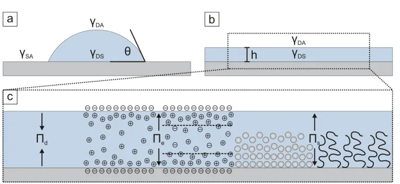
1.2.1 Wetting Thermodynamics
Liquid deposited on top of a horizontally-oriented solid surface takes one of two
configurations depending on the energies of the interfaces between the drop, the surface, and
the ambient phase, which may be a gas or immiscible liquid. If the sum of the drop-solid and
drop-ambient phase interfacial energies is larger than the solid-ambient phase interfacial
contact line, as depicted in Figure 1.1a. Otherwise, the drop will spread and flatten to
completely cover the solid in the form of a wetting film, as in Figure 1.1b. The corresponding
energies can be compared by calculating the spreading parameter
SA DS DA
S (1.1)
where γSA, γDS, and γDA are the solid-ambient, droplet-solid, and droplet-ambient phase
interfacial energies, and the partial wetting and complete wetting states are represented by S < 0 and S > 0. The contact angle at the periphery of a partially wetting drop is given by the Young equation,
cos
SA DS
DA
(1.2)
The forces governing the thickness of the film in a complete wetting state are discussed in the
next section.
1.2.2 Disjoining Pressure
The thickness of a wetting film is determined by the disjoining pressure that arises
from the intermolecular forces between the solid surface and the free interface where the film
and the ambient phase meet. The disjoining pressure Π may have dispersion Πd, electrostatic
Πe, and structural Πs components which can be considered additive such that
d e s (1.3)
Examples of forces that contribute to the disjoining pressure are depicted in Figure 1.1c.
The dispersion contribution to the disjoining pressure arises from the van der Waals
interactions in the system and, for a planar film, can be calculated using
6
d A
h (1.4)
where A is the Hamaker constant, which accounts for the dielectric properties of the phases, and h is the distance between the film surfaces.13 The van der Waals forces are repulsive, with A < 0, only if the film has an intermediate dielectric permittivity relative to the ambient and solid phases. Otherwise, and as is typically true, the forces are attractive, with A > 0, and the dispersion component of the disjoining pressure acts to thin the film.
The electrostatic component of the disjoining pressure is a result of an osmotic effect
driven by accumulation of charges at the film surfaces. The charges may result from
dissociation of ions from the solid surface or adsorption of species to the solid from the
liquid. The fixed charges at the surfaces are balanced by bound and mobile counterions in the
counterions ρ and the electrical potential ψ at any distance x from the midpoint of a film between two identically charged surfaces are given by the Poisson-Boltzmann equation,
2 0 2 0 0 ze kT ze d ze e
dx (1.5)
subject to the boundary conditions
0 0 d
dx (1.6)
2 0 h d dx
(1.7)
where z is the ion valency, e is the charge of an electron, ε is the dielectric constant of the film, k is the Boltzmann constant, T is the temperature, σ is the surface charge density, and the subscripts 0 and h/2 denote the midplane of the film and the film surfaces, respectively.13 The solution to eq 1.5 is
2
log cos
kT
Kx
ze (1.8)
where
2 0 2 0 2 ze KkT (1.9)
The entropy of the system is increased by the diffusion of the counterions away from the
surface and each other, and, thus, the film becomes thicker as the surface charge and the
concentration of counterions increase. For a film of pure liquid, the repulsion can be
calculated from the osmotic pressure using
0
where ρ0 can be determined from the Poisson-Boltzmann equation if h and σ are known.13 Most films contain electrolyte, and the additional ions from their dissociation
suppress some of the repulsive effects of the counterions. The charge distribution and
electrical potential of the film may still be described by the Poisson-Boltzmann equation as
long as terms are added for each ionic species i such that
2 2 0 i i i z e d dx
(1.11)Approximations are required to calculate the repulsion from this more complex version of the
Poisson-Boltzmann equation. The most commonly used is the Guoy-Chapmann theory,13
which gives 2 2 64 tanh 4 h h e ze kT e kT
(1.12)
Here, ρ∞ is the concentration of electrolyte far from the surface and
1 2 2 2
0 i i i e z kT
(1.13)The Debye length 1
approximates the distance that the counterion layer extends from thesurface.
An additional complicating factor for wetting films is that the solid-liquid and
liquid-ambient interfaces likely have different potentials while the standard models assume a
using approximate analytical equations14 or numerical solutions15 for the Poisson-Boltzmann
equation.
Structural contributions to the disjoining pressure exist because of steric effects of the
molecules in the film or ordering of the molecules. The effects are typically short ranged,
acting within a few molecular diameters of the surface, and include the oscillatory force, the
hydration force, the hydrophobic force, and polymer interactions. The oscillatory force arises
from the tendency of molecules to align at a solid surface. The molecules become oriented
such that they are most likely to be located with their centers at the distance from the surface
matching the molecular radius with decreasingly well aligned layers extending out from the
surface. If the film thickness is no greater than a few times the diameter of the molecules, a
pressure arises between the film surfaces that is either repulsive or attractive if the thickness
is a multiple of the size of the molecules and thus promotes ordering of the molecules into
layers and a low entropy state or if the thickness is between multiples of the size of the
molecules and thus disrupts the ordering and promotes a high entropy state.13
The disjoining pressure becomes predominantly repulsive or attractive with high or
low affinity of the molecules in the film for the surface, which enhances or suppresses the
ordering.13 Hydration forces are active when the surface is hydrophilic and the molecules in
the film have ionic groups or hydrogen bonding groups that engender a high affinity between
the liquid and the surface. Hydrophobic forces drive the film surfaces together and the liquid
out if the surfaces and liquid have low affinity for each other.
Polymers that are grafted or adsorbed to the surfaces can promote either film
solvent for the polymer, the polymer will extend into the film and prevent thinning by steric
replusion. If the liquid is a poor solvent, the polymer will form a coil and the surfaces may be
attracted to each other by the hydrophobic force. If the polymer has affinity for both surfaces
but is initially attached to only one surface, it may form attractive bridges by attaching to the
opposite surface.
1.2.3 External Forces
In some systems, external forces may affect the film thickness. Gravity acts on every
practical system, but it is likely to be insignificant for most thin wetting films. The Bond
number evaluates the ratio of gravitational to surface forces in a system and is given by
Bo gh
(1.14)
where Δρ and γ are the density difference and interfacial tension between the film and the
ambient phase and g is the gravitational acceleration. Even for a horizontally-oriented thick film in air and with low interfacial tension, assuming Δρ = 1000 kg/m3, h = 100 μm, and γ = 1 mN/m, Bo = 0.1, while gravity is assumed to be insignificant for Bo < 1.
In contrast, an electrical field applied normal to the film surface may be sufficiently
strong to affect the shape and thickness of the film. If a film is supported on an electrode, the
liquid can be attracted to a second oppositely charged or polarized electrode some distance
above the film.16,17 The effect arises from charge accumulation at the surface of a conducting
film or polarization of an insulating film, and may result in semispherical deformations in the
surface of the film. Other electric field effects, which may be useful as a means of driving
liquid, molecular, or colloidal particle transport in a film, are discussed in the next section.
In some systems, a wetting film may exist in equilibrium with a drop of liquid so that
a meniscus forms where the drop meets the film. A capillary pressure arises from the
curvature of the meniscus that acts to drain the film. The capillary pressure can be calculated
from the Laplace equation
C P
R
(1.15)
where γ is the surface tension of the film and droplet and R is the radius of the meniscus, assuming that the meniscus is linear. In this case, the disjoining pressure is balanced by the
capillary pressure to determine the film thickness.
1.3 Electric Field Effects in Colloidal Systems
1.3.1 Electrophoresis and Electroosmosis
The related effects of electrophoresis and electroosmosis can be employed to
transport colloidal particles through liquid or liquids through capillaries.5 The effects arise
from electrostatic forces acting on surface charges in a dc electric field. A particle suspended
in liquid typically acquires surface charges and is surrounded by a layer of counterions.
When a dc electric field is applied across the system, the counterions partially migrate to the
side of the particle facing the electrode with the opposite charge. The movement of the ions
creates a flow that pushes the particle in the opposite direction, as illustrated in Figure 1.2a.
liquid-filled capillary, the counterions along the charged surface are also drawn toward the
oppositely charged electrode when a dc field is applied. The ions moving along the surface
drag the bulk liquid, engendering a plug flow, as shown in Figure 1.2b. The speed of a
particle or liquid flow is characterized by the electrophoretic or electroosmotic mobility
U E
(1.16)
which relates the velocity of the particle or liquid U to the electric field strength E. The mobility is constant in ideal systems. For particles, the electrophoretic mobility depends on
the ratio of
D where D is the diameter of the particle. At the limit where κ ≪ D, themobility can be estimated using the Helmholtz-Smoluchowski equation
0
(1.17)
where ζ is the zeta potential of the particle, the experimentally measurable electrical potential
at the boundary between the bound and mobile counterions, and η is the viscosity of the
liquid. The same equation holds true for the electroosmotic mobility of a liquid in a capillary.
At the limit where κ ≫ D, the electrophoretic mobility can be estimated using the Hückel-Onsager equation
0 2
3
Figure 1.2. Schematic depiction of the electric field effects that are operative in microscale systems, including (a) electrophoresis, (b) electroosmosis, (c) dielectrophoresis, and (d) electrowetting.
1.3.2 Dielectrophoresis
An alternative method for transporting colloidal particles or liquids is
dielectrophoresis, which affects materials in ac electric fields on the basis of their relative
polarizabilities.8 A particle in an ac field acquires an induced dipole. If the field is
nonuniform, the particle moves into or away from the area of highest field intensity
depending on if the particle is more or less polarizable than the surrounding media. Figure
1.2c depicts a highly polarizable particle in a less polarizable liquid moving to the high
electric field intensity between two electrodes. The dielectrophoretic force on a particle or
droplet is given by the equation
3 2
2
DEP P
F R C E (1.19)
M P M P
C
(1.20)
εP and εM are the dielectric constants of the particle and medium, and E is the electric field
gradient. Dielectrophoresis is advantageous compared to electrophoresis because particles
may be manipulated without also generating electroosmotic flow and because electrolysis
may be avoided by using an ac field.
1.3.3 Electrowetting
Electrowetting is a method for moving liquid and controlling the shapes of droplets
using electric fields. Originally, electrowetting was performed with water on metal
electrodes.10 A voltage applied between the droplet and the electrode causes charges to
accumulate at the liquid-electrode interface and lowers the effective interfacial energy so that
the droplet spreads and wets more of the electrode area. The occurrence of electrolysis limits
the usefulness of this system. More recently, electrowetting has been demonstrated on an
electrode coated by a thin dielectric layer.10,18 The insulator blocks the transfer of charge
from the electrode to the liquid, permitting operation at higher voltages where the effect is
more significant. The voltage drop occurs primarily over the dielectric layer, as the droplet is
assumed to be a perfect conductor. The electric field polarizes the dielectric, increasing its
affinity for the polar water molecules and causing the liquid to spread, as shown in Figure
1.2d. The electrowetting force on the three phase contact line in this configuration, which has
become the most widely used, is given by
2 0
D
where εD and d are the permittivity and thickness of the dielectric layer and V is the applied
voltage. The interfacial energy is effectively reduced by application of voltage as given by
the Lippmann equation
2 0 2
D
EW SD V
d
(1.22)
Reducing the solid-droplet interfacial tension reduces the apparent contact angle of the
droplet. By combining the Young and Lippmann equations, the electrowetting contact angle
is given by
2 0 cos cos 2 D EW SD V d
(1.23)
where θ is the contact angle with no voltage applied.10 However, microscopic observations
have indicated that the contact angle is not changed by application of voltage from the
prediction of the Young equation, but the electric field near the substrate deforms the droplet
to create the macroscopic appearance of contact angle reduction.19
The equations above describe the electrowetting behavior only up to a certain critical
voltage and frequency. Above this saturation voltage, no additional droplet spreading is
observed.10 The effects leading to saturation have not been firmly established. One
hypothesis is that charge trapping in the insulating layer lowers the strength of the electric
field.20 Another is that air is ionized at the droplet contact line, allowing charge to leak from
the liquid and reducing the electrowetting effect.21 Saturation has also been attributed to
deviation from the assumption of a perfectly conducting droplet and a perfectly insulating
frequency at which electrowetting can be performed. Electrowetting is diminished at high
frequencies where the liquid behaves as a dielectric rather than a conductor.10
A critical component of any electrowetting system is the dielectric film. Desirable
coating materials have high dielectric permittivity to maximize the voltage that can be
applied without charge transfer across the insulating layer. The material should also be highly
hydrophobic to achieve a significant difference in droplet shape between the zero voltage and
maximum wetting states. Low contact angle hysteresis is necessary for electrowetting to be
reversible. The most commonly used dielectric materials include amorphous
fluoropolymers,23 parylene,24 and polydimethylsiloxane (PDMS).25 Alternative materials
with higher dielectric constants which can be deposited in thinner layers, such as silicon
dioxide,26 barium strontium titanate,26 and an aluminum oxide layer formed by atomic layer
deposition,27 can reduce the voltage required to achieve similar electrowetting behavior as
seen at higher voltages with thicker insulators. If not natively hydrophobic, dielectric
materials may be coated with a thin layer of fluoropolymer. The contact angle hysteresis can
be reduced by immersing the droplet and substrate in an oil phase which infuses the dielectric
layer.
Electrowetting has found prominent applications in optics, displays, and bioanalytical
devices. A water droplet confined to an oil-filled cell can function as an adjustable optical
lens which can be focused by applying voltage to change the shape of the droplet.28,29 An
electronic reflective display can be created from an array of similar cells. A colored liquid
extensive application of electrowetting, however, has been in the field of droplet-based
lab-on-a-chip devices, which are described in the following section.
1.4 Microfluidics
1.4.1 Applications
Microfluidic devices are miniaturized flow systems in which liquids are confined in
spaces with at least one dimension of less than 1 mm.11 Devices for manipulating small
volumes of liquid have been widely championed as “labs-on-chips” performing chemical and
biological analyses in units with overall dimensions typically at the centimeter scale. A
primary advantage of these systems is that processes can be performed with very small liquid
volumes when reagents are expensive or sample volumes are limited. Miniaturization can
also permit a high number of process steps or duplicate processes to be integrated into one
device, enabling automation of operations and high throughput of samples or assays. Heat
transport is faster in small volumes, reducing the time required for analyses. Microfluidics
may also enable techniques that are simply not possible in larger-scale systems, such as
probing individual cells or molecules, while taking advantage of the unique physics of
microscale flows, as discussed in the following section.
Many types of bioanalytical operations have been demonstrated in microfluidic
devices. The typical device consists of a channel through which the sample flows between
mixers, reaction chambers, separation structures, and detection points where the steps
required for the analysis occur. Often the process begins with sample treatment, such as
reaction (PCR).33,34 Reactions may occur as liquids flow through channels or are held in
larger chambers. The most common separation technique employed in microfluidic devices is
electrophoresis, which can be used to separate molecules of different sizes or charges.32–35 By
applying the electric field perpendicularly to the flow and positioning outlets for different
size molecules at the end of the channel, continuous separations may be performed.36 The
sieving matrix may be microfabricated into the device in the form of an array of posts.37,38
Virtual posts can be created using dielectrophoresis to repel molecules from the area over an
electrode.39 Bacteria40 and viruses41 can be collected on electrodes by dielectrophoresis.
Different cell types can be separated by optical trapping42 or dielectrophoresis.43,44 Cells may
be sorted into different channels by switching valves in response to fluorescence readings of
individual cells.45 Detection of separated species may be achieved by fluorescence or
electrochemical46 potentials. Immunassays47 and DNA hybridization assays40,48 have also
been demonstrated. Although most lab on a chip devices are targeted for bioanalytical
applications, chemical synthesis and purification may also be performed.49
Many microfluidic devices have been developed for synthesis of micro- and
nanoparticles in addition to lab-on-a-chip applications. Microfluidic reactors for the synthesis
of metallic nanoparticles50–52 and silica colloidal particles53 allow precise control over the
timing and temperature of the reaction, yielding particles with tight size distribution.
Microfluidic devices that generate droplets are particularly applicable for particle synthesis if
the droplets can be solidified.54 Droplets containing monomer may undergo UV55 or
crystallization.55 Particles may also be created from aqueous gels57 and low temperature
melting metals.54 Shape anisotropic particles may be produced by confining the droplets in
channels of different height and width during polymerization.54,58 By an alternative method,
polymer particles may be created directly in a continuous stream of monomer by UV
polymerization with a masked illumination source.59 Particles of any shape or pattern
matching an opening in an opaque mask will solidify in the liquid stream when the stream is
illuminated by light through the mask.60
Particles with a variety of complex compositions may be produced by microfluidic
devices. Chemically anisotropic particles may be produced by combining two adjacent
streams in droplet-generating61,62 or masked photopolymerization63 devices so that the
resulting droplets and particles consist of two halves made of different materials. Multiple
emulsions can be produced by performing a set of droplet-generating steps in series.64,65 For
instance, a water-in-oil-in-water emulsion may be formed by first generating a sequence of
water droplets in an oil stream, and then, from that oil stream, splitting off a series of droplets
in a second water stream.64 Such devices may be used to produce particles with polymer
vesicles66,67 that may be useful for transporting cells and proteins by encapsulation68 or
particles with magnetic cores.69
Other less widely implemented applications of microfluidic devices have also been
demonstrated. Microfluidic heat exchangers based on channel flow70,71 and droplet
transport72 have been constructed. The small sizes of these devices makes them well suited
for cooling integrated circuits. The thin dimensions of microfluidic channels enable even
be continuously replenished with chemicals and may be useful for applications such as
culturing biological tissues.74 If the liquid in the microchannels is polymerizable, the
channels can act as a rigid skeleton for a shape-memory material.75 Microfluidic devices may
have optical applications including tunable waveguides76 and filters.73 Liquid-based
computers employing microfluidic architectures have even been proposed,77 in which
droplets in highly repetitive channel structures may act as data bits.78
1.4.2 Physics of Microscale Flow
Microscale flow is dominated by viscous and surface forces. One consequence is that
the flow is laminar, in contrast to flows of larger volumes, in which inertia leads to turbulent
mixing between flow streams with random trajectories. The absence of convection in
microfluidic systems means that liquid mixing occurs only by the slower process of diffusion
between adjacent, parallel flow streams.11 Laminar flow in microfluidic devices may enable
some processes that are not possible in larger scale systems. For instance, fast-diffusing
molecules may be separated from slow-diffusing molecules or particles from one stream into
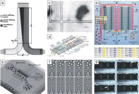
an adjacently flowing clean stream,79 as depicted in Figure 1.3a. Separations may be
performed by transferring particles between coflowing streams using hydrodynamic forces,80
optical trapping,42,81 dielectrophoresis,43,44 magnetophoresis,82 or acoustic waves,83 as Figure
1.3b illustrates. Conversely, if different species in two separate streams diffuse together and
interact or react, the process can be monitored spatially and quantified.84 The effects of
cells in parallel flows.85 Surface patterning86 and materials fabrication87 can be performed at
high precision by reaction at the interface between streams containing different reagents.
The laminar flow, on the other hand, presents challenges when rapid mixing and
reaction are desired.11 Significant efforts have been made to develop methods for enhancing
mixing of liquids in microfluidic devices. Mixing can occur passively as liquids move
through specially designed device structures. In a simple example, liquids can be mixed by
pumping through a loop. Because the liquid at the center of the channel moves faster than the
liquid at the channel walls in pressure-driven flow, the interfacial area between two segments
of liquid increases as the liquids travel around the loop together, and the distances required
for complete mixing to be achieved by diffusion become smaller.88 Serpentine channel
routes89 and grooves90 or wells91 in channel walls may deform the interface between two
coflowing liquids, causing liquid layers to fold over each other and reducing the distance
required for diffusive mixing between the two liquids, a process termed chaotic advection.
Individual reactions may be confined to droplets92,93 or segments of liquid between bubbles94
in which circulating flows are engendered by shear as the droplets or segments move along
the device walls or a fluid boundary with a viscosity gradient. Active mixing strategies, in
which external energy is imparted to the system, have also been demonstrated and include
using ultrasonic vibrations95 and electric and magnetic field-induced flow vortices.96–99
Microfluidic devices are also characterized by high surface-area-to-volume ratios,
which have significant implications for actuating and directing liquid flow. If the surfaces are
charged, electroosmotic flow may be induced. Flows can be confined to specific pathways on
along surface energy gradients that are fixed103 or controllable by thermal,104 electrical,105
electrochemical,106 or light-based107 mechanisms. Liquid can also be moved by capillary
forces imposed by the geometry of the device.108
1.4.3 Microfabrication
Early microfluidic devices were made using the photolithography and etching
methods developed by the integrated circuit industry and were fabricated from silicon33,36 or
glass.35 An example of such a device is pictured in Figure 1.3c. An advantage of this class of
techniques and materials is that fluidic channels with dimensions smaller than 100 nm can be
produced readily. However, to create nanoscale features, electron-beam109 or interferometric
lithography110 must be used instead of standard photolithography, or a focused ion beam111 or
laser112 must be used to directly etch the channels into the surface. These lithography-based
methods require multiple complex processing steps, expensive equipment, and clean room
facilities.
More economical microfluidic devices have been made from polymer materials, for
which simpler and lower cost processing methods are available. One common method is soft
lithography, whereby a reusable inverse mold of the desired channel structure is fabricated by
traditional photolithography and filled in with a liquid elastomer, usually PDMS, which is
then cured and removed from the mold.113,114 The method has the advantage of being easy to
perform with no complex equipment required after the initial mold is produced. Another
method is hot embossing,115 which may also be called nanoimprint lithography116 or
step-and-flash imprint lithography.117 In these techniques, the mold is pressed into a liquid
polymer coating on a substrate, and the polymer is cured by cooling below the glass
transition temperature or photopolymerization by exposure to UV light. Closed channels can
be formed by vapor deposition of material over the trenches in the polymer.118 Injection
cycloolefins is more suitable for mass production of microfluidic devices at low cost but
requires a large initial investment in machinery.119–120
Polymer surfaces can be modified by a variety of means to attain properties desirable
for a particular application. Microfluidic devices are often enhanced by rendering polymers
more hydrophilic than their native states because filling the devices with aqueous solutions
becomes easier and liquid transport by electroosmosis becomes more efficient with charged
channel walls. Also, hydrophilic surfaces are resistant to fouling with biomolecules that may
adsorb due to hydrophobic interactions. In other applications, such as for culturing cells, it is
desirable to immobilize proteins on device surfaces.121,122 Chemical modification of
polymethylmethacrylate and polycarbonate to make more hydrophilic microchannels has
been described.123,124 Much of the work on controlling surface properties has focused on
PDMS. Silane chemistry has been used to obtain PDMS materials with a range of surface
energies.125 Silica filler material and ion adsorption have been speculated to be sources of
surface charge on PDMS.126,127 Oxygen plasma128 and ultraviolet/ozone129 treatments, which
create silanol groups, are popular methods for hydrophilization of PDMS. Addition of
surfactant to the liquid in the device can also make the surfaces more wettable, enhance
electroosmotic flow,130,131 and minimize fouling by biomolecules.132 Surface
functionalization by chemical vapor deposition133 and layer-by-layer adsorption of charged
1.4.4 Device Configurations
Microfluidic devices have been developed in several different formats. The first
devices consisted of systems of closed channels through which sample and reagent liquids
flowed as different operations were performed in series. Flow through the channels has been
driven by electroosmosis35 or external pressure.84 An example of such a device is shown in
Figure 1.3d.
Repetition of channel structures may enable high throughput applications. One unique
type of device in this category is the so-called “LabCD.” This platform features an array of
repeating channel structures arranged in a circle around a thin flat plastic disk. When the disk
is rotated, the centrifugal force drives the liquid through the channels from the center of the
disk to the perimeter.135 This platform may be uniquely well suited for processes that can be
enhanced by strong gravitational-like forces, such as driving liquid through a
chromatography column136 or separating blood components137 before performing an
assay.138,139
Another prominent example of a high-throughput device, shown in Figure 1.3e,
consists of two layers of channels in a soft elastomer. Liquid traveling through the channels
in one layer can be manipulated by deforming with pressurized air the channels in the other
layer.140,141 This type of platform is particularly useful for comparing many different
experimental conditions, such as for protein crystallization,142 cell culture,143 protein
expression by cells,144 and synthesis of chemical libraries.145
Another way to achieve high throughput without repeating channel structures is to
maintained in each droplet, which functions as an individual reactor. Droplets can be formed
at a T-junction146 or by a flow focusing aperture,147 as shown in Figure 1.3f. Droplets can be
combined by merging at a Y-junction148 or split upon reaching a T-junction or a column in
the middle of a channel.148,149 Sorting can be performed by using dielectrophoresis to force
droplets to one or the other outlet of a Y-junction.150 Like the parallel channel devices, a
variety of applications of the droplet devices have been demonstrated, including kinetics
studies,151 protein crystallization,152 cell culture,153 and drug screening,154 with the goal of
comparing a large number of conditions and achieving high throughput.
Another platform for droplet-based microfluidics uses electrowetting to generate and
manipulate droplets. Droplets are contained in a slit between two parallel plates where they
can be transported in two dimensions. One plate has an array of electrodes beneath a thin
dielectric film while the other plate serves as a reference electrode. As the electrodes are
sequentially activated, the droplets preferentially wet the dielectric surface where the voltage
is applied and move along a pathway.105 Droplets stretched over multiple electrodes can be
split by switching off an electrode in the center, while switching on an electrode between two
nearby droplets can cause the droplets to merge. Droplets can be formed by extending a
finger of liquid from a reservoir of liquid along several electrodes and then switching off
electrodes between the reservoir and the desired droplet.155 These operations are shown in
Figure 1.3g. While the throughput permitted by this approach may be smaller than the
platform on which droplets move through channels by pressure, the electrode array scheme
electrowetting microfluidic devices have been used for colorimetric assays,156 enzymatic
assays,157 immunoassays,158 PCR,159 and DNA sequencing.160
1.4.5 Nanofluidics
The trend of miniaturization of flow systems presently involves many research efforts
focused on the nanofluidics regime, which encompasses systems with at least one dimension
below 100 nm. Nanofluidic structures have size scales comparable to the diameters of
macromolecules and the thicknesses of the electric double layers at charged surfaces,
resulting in unique molecular confinement and electrokinetic effects.
The most direct advantage gained by operating at the nanoscale is the ability to
perform chemical and biochemical operations with liquid volumes that can be small enough
to isolate individual molecules. Confining a polymer to a space narrower than the size of its
coiled state leads to extension of the molecule. Such stretching of DNA has permitted
analyses on single molecules including measuring length,161 detecting interactions with
single proteins,162 and restriction mapping.163 Base sequencing of individual DNA strands
may soon be accomplished in nanofluidic devices.164 Gaps smaller than molecular diameters
can also enable separation of discrete numbers of molecules, either by steric exclusion of
larger molecules165 or by forcing molecules to adopt less entropically favorable
conformations, for which the probability of occurrence depends on molecular size.166
The high surface-area-to-volume ratio of nanoscale flow systems means that surface
charges dominate transport and electrokinetic processes, a unique effect which can be
the channel diameter approaches the thickness of the layer of counterions screening the
surface charges, molecules with the same charge as the surface are repelled to the center of
the channel, and species of charge opposite to the surface are attracted to the channel wall.167
Because the velocity profile through the counterion layer is parabolic, the species at the
center of the channel flow faster than species at the wall. In very small channels, molecules
with the same charge as the surface may be excluded from the channel entirely.168 More
sophisticated nanofluidic devices can actively direct separations by using electrodes rather
than surface charge to control the electrical potential in the channel.169
1.5 Colloidal Self-Assembly
1.5.1 Applications
Colloidal crystals are materials with micro- or nanometer periodic ordering. Features
of sub-micrometer resolution can be fabricated by top-down methods including
photolithography, soft lithography, and embossing170-171 as described in the previous section
for microfluidic devices. However, these techniques typically require multiple processing
steps and expensive equipment. An elegant alternative is bottom-up self-assembly of
colloidal particles. Micro- or nanoparticles spontaneously form repeating structures under the
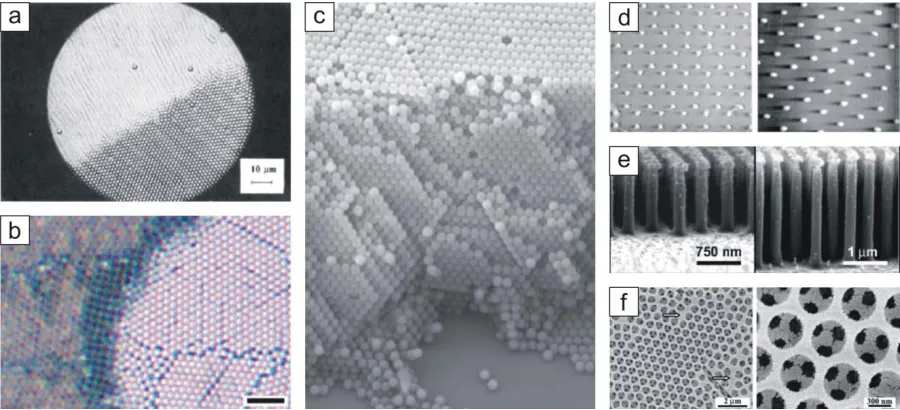
right balance of attractive and repulsive external and intermolecular forces, as shown in
Figures 1.4a–c. The typical building blocks for colloidal crystals are metallic nanoparticles
and polystyrene and silica microspheres. The resulting materials are being used in a variety
Colloidal crystals have received most attention because of their unique optical
properties. It is often envisioned that colloidal crystals can serve as photonic band gap
materials blocking penetration by light of certain wavelengths corresponding to crystal
periodicity.172–174 By introducing designed defects into the crystals, integrated circuits for
light waves instead of electrons may be created. These photonic circuits require formation of
defect-free crystals which is practically difficult, so this application remains futuristic.
However, colloidal crystal coatings for other optical applications may find more immediate
use. Tunable diffraction gratings can be created by embedding a colloidal crystal in a
polymer matrix that can swell and contract to adjust the spacing of the periodic ordering.175
Colloidal crystals can also function as antireflective coatings.176 When the periodicity of the
crystal is smaller than the wavelength of light, the refractive index of the material may be
taken as the average of the particles and the space between, enabling calibration of the
refractive index on which the reflective characteristics of the material depend. These coatings
have been shown to improve the efficiency of solar cells.177
Colloidal crystals can also serve as templates for fabrication of other microstructures.
To create surface patterns and textures, metal can be evaporated178,179 or the substrate can be
etched178,180 in the spaces between the particles of a deposited colloidal monolayer, which
can be subsequently removed. Figures 1.4d–e show a surface patterned with metal and an
array of pillars, respectively, produced by such colloidal crystal lithography masks. Colloidal
crystals can also serve as templates for more complex three-dimensional porous structures. In
this case, the interstitial space between polymer spheres comprising a crystal is filled in with
network. Subsequent dissolution of the polymer spheres leaves a porous structure with
periodic order, as shown in Figure 1.4f. The large surface area presented by such materials
makes them useful as catalysts or sensors.183 In particular, these materials have demonstrated
promise as surface enhanced Raman spectroscopy substrates exhibiting enhanced and
repeatable absorbance.184,185 Formation of a colloidal crystal at an emulsion droplet interface
instead of on a solid substrate is a technique for creating shells that can encapsulate drugs or
cells.186
Colloidal crystals can function as chemical sensors if the constituent particles are
functionalized with molecules or embedded in hydrogels that change size in the presence of
specific chemicals. Variation in the interparticle spacing can change the electrical resistance
of the crystal187 or the color by changing the wavelength of light diffracted by the crystal.188
Antibody-189 or DNA-mediated190 interactions that cause conductive particles to coagulate
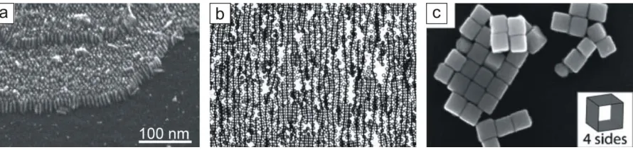
Figure 1.4. Images of colloidal assemblies, including (a) microspheres packing into a crystalline monolayer by convective assembly,220 (b) the transition from a bilayer to a monolayer of microspheres in a colloidal crystal coating,225 (c) a three-dimensional photonic crystal,260 (d) a metal pattern evaporated179 and (e) microscale pillars etched180 on surfaces using colloidal crystal lithography masks, and (f) a porous microstructure with periodic ordering templated by a colloidal crystal.261
1.5.2 Assembly Driven by External Fields
In a gravitational field, colloidal particles that are sufficiently large eventually settle
out of suspension. As they accumulate, the particles adopt a face-centered cubic191 or
hexagonal close packed arrangement.192-193 Substrates with microscale holes194,195 or
grooves196 or patches patterned with charged molecules197 can be used to control the
locations of particles on the substrate and nucleate the growth of a single-domain colloidal
crystal. Centrifugation may be used to accelerate the settling of the particles, but the time
scale for the process remains hours.198,199
Electrophoresis has been used to draw particles more rapidly to an electrode surface
cause the particles at the surface to move laterally toward each other, enhancing the
packing.202 Patterns of crystals on surfaces can be created by illuminating a transparent
indium tin oxide electrode with light in the desired crystal shape. The light increases the
current density and, thus, the electrophoretic force in the illuminated areas.203 Similar to
electrophoresis, a magnetic field may be used to drive assembly of crystals from magnetic
particles.204,205
Particles may be collected between planar electrodes by dielectrophoresis.206 This
force acts on almost any type of particle, charged or uncharged, making dielectrophoretic
assembly potentially widely applicable. The electric field induces dipoles in the particles
because the polarizability of the counterionic layer around the particle surfaces is larger than
the polarizability of the particles or the surrounding media. The dipoles induced by the
electric field cause the particles to align in chains207 which can then pack into single-domain
crystals.208 Dielectrophoresis has also been demonstrated to cause metallic nanoparticles to
concentrate and aggregate linearly between the electrodes, forming a microwire and bridging
the gap.209,210 Projection of an optical image onto a light sensitive electrode can create high
resolution electric fields with individual regions of electric field intensity maxima to
independently position thousands of particles in an array.211 Smaller numbers of individual
particles may also be positioned by optical trapping in a laser beam.212
1.5.3 Assembly Driven by Solvent Flow
Techniques relying on solvent flow to concentrate particles have also been
organize into hexagonally close packed planes in shear flow so that the particles can move
more easily past each other. Oscillatory shear flows may assist in the formation of
single-domain crystals.213 Shear-ordered colloidal crystal coatings can be deposited by spin
coating.215,216
Particles adsorbed to a liquid interface can be compressed into a two-dimensional
ordered structure using a Langmuir trough.217 The floating crystal layer formed by this
method can be transferred to a solid substrate that is withdrawn from the liquid phase.218,219
The most widely studied assembly technique based on flow is convective assembly.
In this method, evaporation of the liquid medium from a suspension of particles engenders a
flux in the liquid that transports the particles to the substrate-liquid-air contact line, as can be
seen in the upper left of Figure 1.4a. There, attractive capillary forces may assist the
accumulating particles in forming a close-packed array.220 The convective assembly
mechanism is responsible for the ring of particles that forms as a sessile droplet of a
suspension evaporates, the so-called “coffee ring effect.”221 By vertically dipping a substrate
into a dilute particle suspension and slowly withdrawing it222,223 or by immersing a substrate
in a particle suspension and allowing the suspension medium to evaporate completely,224 a
large uniform crystal coating can be deposited on the substrate by convective assembly. A
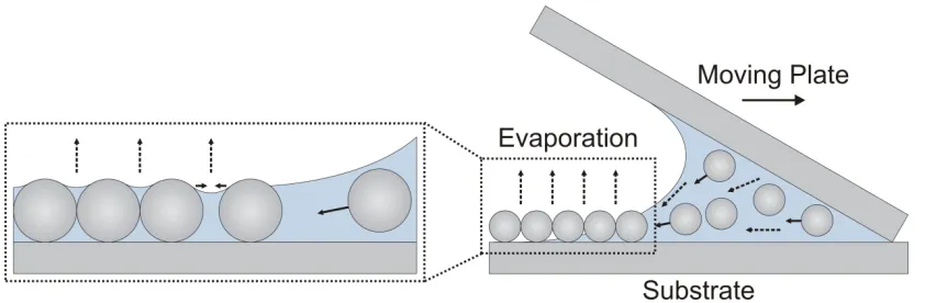
more rapid and better controlled method of crystal coating deposition has been engineered by
pinning a high volume fraction particle suspension in a wedge and dragging it across a
horizontally oriented substrate, as illustrated in Figure 1.5.225 The structure of the coating can
vary from submonolayer to a few complete layers, as shown in Figure 1.4b. The height of the
concentration, evaporation rate, or drying length increase. The method is applicable to a
variety of types of particles including polystyrene microspheres,225 metallic226 and
inorganic227 nanoparticles, virus particles,228 and live cells.229
Figure 1.5. Schematic of convective assembly coating deposition process. A suspension of colloidal particles is pinned between two plates and dragged across the substrate. Evaporation from the thin film at the trailing meniscus of the suspension droplet drives particle transport to the growing crystal coating in the film. As particles accumulate in the film, they adopt a hexagonal close packed structure assisted by capillary forces.
1.5.4 Assembly Driven by Molecular Interactions
Molecular linkers can be used to bind particles to each other to create colloidal
assemblies. This approach is generally applied to particles in the nanometer size range, where
the ratio of surface-area-to-particle-mass is high. Synthetic polymers,230 complementary
DNA strands,231,232 and antibody-antigen relationships233 have been used to bind particles
together to form larger structures. Additional synthetic linkers which are sensitive to
light,234,235 temperature236,237 solvent polarity,238,239 pH237,240,241 and electrochemical
without crystalline ordering, a limitation to the technique. However, DNA linker molecules
with precisely tuned sequence and length have been shown to lead to crystalline
ordering.243,244 Linker molecules can be used to regulate the spacing between particles,
providing a means to tune the optical properties.245
1.5.5 Assembly with Anisotropic Particles
A richer variety of microstructures can be assembled from anisotropic particles. For
instance, assembly of particles having nonspherical geometries including ellipsoids,246
rods,247–249 viral rods,228 peanuts,250 and pentagon-shaped particles251 can result in one-, two-,
and three-dimensional structures that are not achievable with simple spherical particles alone.
A multilayer assembly of rods is shown in Figure 1.6a. Electric252 and magnetic253 fields can
be used to align ellipsoidal particles in one direction during assembly, resulting in materials
with directionally dependent properties. Material or chemical anisotropies may also be used
to direct the way that particles align and organize. Spherical particles with a dielectric core
and one side coated with a metallic254 or magnetic255 layer form chains as well as two- and
three-dimensional structures with the coated sides of the particles facing each other when an
electric or magnetic field is applied, as shown in Figure 1.6b. Particles with surface energy
anisotropy can be oriented at a liquid interface.256 Selective chemical modification can define
which regions of the particles are attractive to each other and thus control the arrangement of
the final structure257,258 or the order of a multistep assembly.259 Figure 1.6c shows how cubic
Figure 1.6. Images of colloidal assemblies from anisotropic particles, including (a) rod-shaped particles assembled into a colloidal crystal,249 (b) metallodielectric Janus particles that assemble in staggered chains with metal sides facing,254 and (c) cube-shaped particles that assemble into sheets because only 4 sides are functionalized to be attractive.258
1.6 Overview of Dissertation
Three new systems in which electric fields govern the shape of and flow in wetting
films are described in the following chapters. In Chapter 2, an improved method of
convective assembly of colloidal crystal coatings that incorporates electrowetting is
discussed. Applying voltage during the coating deposition causes the film in which the
particles assemble to be extended. The rate of assembly and homogeneity of the crystal are
increased, and the process is explained using a model. Chapter 3 explains the behavior of
wetting films between droplets and microfluidic device surfaces when electrowetting is used
to move the droplets. While the motion of the droplets entrains liquid in the films, the electric
field tends to thin the films. The effects of these competing forces are characterized on the
basis of the applied voltage, ac frequency, and addition of surfactants to the system. Then, in
Chapter 4, a nanoscale flow system based on electroosmosis in wetting films with
thicknesses of tens of nanometers is described. The liquid flows over an open surface and is