University of Windsor University of Windsor
Scholarship at UWindsor
Scholarship at UWindsor
Electronic Theses and Dissertations Theses, Dissertations, and Major Papers
2009
Implementation and Evaluation of an NoC Architecture for FPGAs
Implementation and Evaluation of an NoC Architecture for FPGAs
Thuan Le
University of Windsor
Follow this and additional works at: https://scholar.uwindsor.ca/etd
Recommended Citation Recommended Citation
Le, Thuan, "Implementation and Evaluation of an NoC Architecture for FPGAs" (2009). Electronic Theses and Dissertations. 8077.
https://scholar.uwindsor.ca/etd/8077
Implementation and Evaluation of an
NoC Architecture for FPGAs
By
Thuan Le
A Thesis
Submitted to the Faculty of Graduate Studies through Electrical and Computer Engineering in Partial Fulfillment of the Requirements for the
Degree of Master of Applied Science at the University of Windsor
1*1
Library and Archives CanadaPublished Heritage Branch
395 Wellington Street OttawaONK1A0N4 Canada
Bibliotheque et Archives Canada
Direction du
Patrimoine de I'edition
395, rue Wellington Ottawa ON K1A 0N4 Canada
Your We Votre inference ISBN 978-0-494-82086-5 Our file Notre r6f6rence ISBN 978-0-494-82086-5
NOTICE: AVIS:
The author has granted a
non-exclusive license allowing Library and Archives Canada to reproduce, publish, archive, preserve, conserve, communicate to the public by
telecommunication or on the Internet, loan, distribute and sell theses
worldwide, for commercial or non-commercial purposes, in microform, paper, electronic and/or any other formats.
L'auteur a accorde une licence non exclusive permettant a la Bibliotheque et Archives Canada de reproduce, publier, archiver, sauvegarder, conserver, transmettre au public par telecommunication ou par I'Internet, preter, distnbuer et vendre des theses partout dans le monde, a des fins commerciales ou autres, sur support microforme, papier, electronique et/ou autres formats.
The author retains copyright ownership and moral rights in this thesis. Neither the thesis nor substantial extracts from it may be printed or otherwise reproduced without the author's permission.
L'auteur conserve la propnete du droit d'auteur et des droits moraux qui protege cette these Ni la these ni des extraits substantiels de celle-ci ne doivent etre imprimes ou autrement reproduits sans son autorisation
In compliance with the Canadian Privacy Act some supporting forms may have been removed from this thesis.
Conformement a la loi canadienne sur la protection de la vie pnvee, quelques formulaires secondaires ont ete enleves de cette these.
While these forms may be included in the document page count, their removal does not represent any loss of content from the thesis
Bien que ces formulaires aient inclus dans la pagination, il n'y aura aucun contenu manquant
© 2009 Thuan Le
All Rights Reserved. No Part of this document may be reproduced, stored or otherwise retained in a retrieval system or transmitted in any form, on any medium by any means
Authors Declaration of Originality
I hereby certify that I am the sole author of this thesis and that no part of this thesis
has been published or submitted for publication.
I certify that, to the best of my knowledge, my thesis does not infringe upon
anyone's copyright nor violate any proprietary rights and that any ideas, techniques,
quotations, or any other material from the work of other people included in my thesis,
published or otherwise, are fully acknowledged in accordance with the standard referencing
practices. Furthermore, to the extent that I have included copyrighted material that
surpasses the bounds of fair dealing within the meaning of the Canada Copyright Act, I
certify that I have obtained a written permission from the copyright owner(s) to include
such material(s) in my thesis and have included copies of such copyright clearances to my
appendix.
I declare that this is a true copy of my thesis, including any final revisions, as
approved by my thesis committee and the Graduate Studies office, and that this thesis has
Abstract
The Networks-on-Chip (NoC) approach for designing Systems-on-Chip (SoC) is currently
emerging as an advanced concept for overcoming the scalability and efficiency problems of
traditional bus-based systems. A great deal of theoretical research has been done in this
area that provides good insight and shows promising results. There is a great need for
research in hardware implementation of NoC-based systems to determine the feasibility of
implementing various topologies and protocols, and also to accurately determine what
design tradeoffs are involved in NoC implementation. This thesis addresses the challenges
of implementing an NoC-based system on FPGAs for running real benchmark applications.
The NoC used a mesh topology and circuit-switched communication protocol. An
experimental framework was developed that allowed implementation of NoC-based system
from a high level specification, using the Celoxica Handel-C hardware description
language. Two test applications: charged couple device (CCD) and JPEG were developed
in Handel-C to be used as our benchmark applications. Both benchmarks are
computational expensive and require large quantities of data transfer that will test the NoC
system. Implementation results show that the NoC-based system gives superior area
utilization and speed performance compared to the bus-based system, running the same
Acknowledgements
I would like to express my sincere gratitude to my supervisor, Dr. Mohammed A. S.
Khalid, where my research would not be possible without his advice and wisdom that
guided me over the course of this research. Dr. Khalid, who first offered an undergraduate
course in reconfigurable computing for embedded system had introduced me to this
exciting field. For this very reason, it had moth ated me to continue my academic career in
this field. My appreciation also goes out to my thesis committee members. Dr. K. Tepe and
Dr. A. Ngom, for their time to sit on my committee and for reviewing my thesis.
I want to thanks my parents, for their constant support, encouragement, and to
remind me every day to make time to eat. Thanks to my brothers (Steven and David) and
sisters (MyLai and Dianna) for all those time I pester around when my research feels
overwhelming.
Finally, I need to acknowledge my friends and fellow graduate students at the
University of Windsor. Dat, Gordon, Jason. Omesh, Geraldo, and David, thank you for
your friendship and for amusing me with your \ arious stories. Ngan, I always enjoyed our
conversation and how we continue to motivate each other as we pursuit our own graduate
study. Thanks to Omar, Marwan, Junsong and Aws for your company and making those
long days at the office more enjoyable. Lastly, thanks to the rest of my colleagues: to
Hongmei, Matt, Mike, Liton, Yasser. Lin Lin, Carl. Neil, Anthony. Ashkan and everyone
Table of Contents
Author's Declaration of Originality iv
Abstract v
Acknowledgements vi
List of Figures xi
List of Tables xiii
List of Abbreviations xiv
1 Introduction 1
1.1 Thesis Objectives
-1.2 Thesis Organization 3
2 Background and Previous Work 4
2.1 Overview of NoC 4
2.1.1 NoC Building Blocks 4
2.1.2 NoC Architecture 5
2.2 FPGA Technology 9
2.3 Soft-core Processors 12
2.3.1 Nios II Soft-core Processor 13
2.3.2 MicroBlaze II Soft-core Processor 13
2.5 Summary 16
3 NoC Architecture 17
3.1 Topology 17
3.2 Protocol 19
3.2.1 Physical Layer 19
3.2.2 Data Link Layer 20
3.2.3 Network Layer 21
3.2.4 Transport Layer 21
3.3 Data Transactions 21
3.4 Quality of Service 22
3.5 Summary 23
4 The Proposed NoC Design 24
4.1 Router 24
4.1.1 Partial-Crossbar Design 26
4.1.2 Crossbar Configuration 29
4.2 Configuration Block 34
4.2.1 Primary latency 34
4.3 Network Adaptor 35
4.4 Links 35
4.5 Summary 36
5 Experimental Evaluation Framework 37
5.1 NoC Specification and Implementation Methodology 37
5.1.1 Communication Infrastructure 38
5.1.2 Communication Paradigm 39
5.1.3 Application Mapping 40
5.1.4 Celoxica Handel-C 40
5.2 Xilinx MicroBlaze Soft-Core Processor 41
5.2.1 On-Chip Peripheral Bus 42
5.3 Charged-Couple Device Benchmark 43
5.3.1 Pure software system 45
5.3.2 Bus-based system 45
5.3.3 NoC-Based Implementation of a Microblaze System 47
5.4 JPEG Benchmark 48
5.4.1 Pure software system 48
5.4.2 Bus-based system 49
5.4.3 NoC system 49
5.5 Summary 50
6 Comparison of NoC-Based System and Bus-Based System 51
6.1 Processing Cycle 51
6.1.1 CCDBM Processing Cycle 51
6.1.2 JPEG Processing Cycle 54
6.2 Implementation Results 55
6.2.1 Area Results 55
6.2.2 Speed Results 59
6.3 Summary 59
7 Conclusions and Future Work 61
7.1 Summary of Research Contributions 62
7.2 Future Work 62
Appendix A 64
Simulating a real CCD 64
A.1 CCD Module in C 66
A.2 CCDPP |Module in C 67
A.3 UART Module in C 68
A.4 CODEC Module in C 69
A.5 CNTRL module in C 71
A.6 MAIN Module in C 72
References 73
List of Figures
Figure 2.1: Hardware Components of an NoC [4]
Figure 2.2: Shared-Medium Networks: a Traditional Bus-Based System.
Figure 2.3: Direct networks: (a) Mesh, (b) Torus, and (c) Hypercube
Figure 2.4: Indirect Networks (adapted from [1])
Figure 2.5: Schematic for a Generic FPGA Logic Element (LE) [14]
Figure 2.6: Schematic of a Lookup Table (LUT) [3]
Figure 2.7: Generic FPGA Routing Architecture
Figure 3.1: 2-Dimensional Mesh Topology
Figure 3.2: Port Interface
Figure 3.3: Data Transmission Handshake Protocol
Figure 4.1: Block diagram of a Router [9]
Figure 4.2: Cascading Intermediate Partial Crossbars
Figure 4.3: Partial Crossbar
Figure 4.4: Crossbar Interconnection
Figure 4.5: Routing South Port to Core Port
Figure 4.6: Configuration Control Word 30
Figure 4.7: Example of a Test Scenario
Figure 4.8: Crossbar Configuration Block 34
Figure 4.9: Block Diagram of Network Adaptor
Figure 5.1: Design Space for NoC Architectures [2] 38
Figure 5.3: Microblaze Bus Configurations 41
Figure 5.4: Integration of MB and Handel-C Slaves with Slaves at the Top-le\ el 1
Figure 5.5: Internal of a CCD [26] 1
Figure 5.6: Flow-Diagram for CCD 1
Figure 5.7: Flow-Diagram of the Executable Model of the CCD [29] 1
Figure 5.8: Integration of MB and CCDBM Slaves Peripherals 46
Figure 5.9: Integration of MB and NoC 1
Figure 5.10: JPEG Encoding Sequence for a Block of 8 x 8 Pixels 1
Figure 5.11: Integration of MB and JPEG Slave Peripherals 1
Figure 5.12: NoC System for JPEG 1
Figure 6.1: Bus-Based Processing Cycle for CCDBM 1
Figure 6.2: NoC-Based Processing Cycle for CCDBM 1
Figure 6.3: Bus-Based Processing Cycle for JPEG 54
Figure 6.4: NOC-Based Processing Cycle for CCDBM 1
List of Tables
Table 4.1: Connections Assignment for Partial Crossbar 27
Table 4.2: Port Conversion Table 30
Table 4.3: Configuration Bits Value for Test Scenario 32
Table 4.4: Connection Assignment for Configuration Block 34
List of Abbreviations
Abbreviation Definition ASIC CAD CB CCD CCDBM CCN CLB CPU CS DOPB DK DLMB DRM DSP FDCT FIFO FPGA GUI HC I/O IC ILMB IOB IP JHDL JPEG LE LUT MB MIN MSIApplication Specific Integrated Circuit Computer Aided Design
Crossbar
Charged Couple Device
Charged Couple Device Benchmark Central Coordination Node
Configurable Logic Block Central Processing Unit Circuit Switched
Data On-Chip Peripheral Bus Design Kit
Data local Memory Bus Digital Radio Mondiale Digital Signal Processing
Forward Discrete Cosine Transform First In First Out
Field Programmable Gate Array Graphic User Interface
Handel-C Input/Output Integrated Circuit
Instruction Local Memory Bus Input/Output Block
Intellectual Property
Java-based Hardware Description Language Joint Photographic Experts Group
Logic Element Lookup Table MicroBlaze
MUX NoC OPB PC PCC PS PLD QoS RAM RISC Rx SoC SOPC SSI Tx UART VC VHDL
Multiplexer Network-on-Chip On-chip Peripheral Bus Personal Computer Packet Connected Circuit Packet Switched
Programmable Logic Device Quality of Service
Random Access Memory
Reduced Instruction Set Computer Receiver
System-on-Chip
System on a Programmable Chip Small Scale Integration
Transmitter
Universal asynchronous Receiver/Transmitters Virtual Circuit
Chapter 1
Introduction
The complexity of a system on silicon is comparable to other macro systems such as
space shuttle or skyscrapers, when measured in terms of the number of basic elements
intricately connected together, but at a micro level. As semiconductor technology evolves,
electronics industry continuously pushes the envelope for greater functional and
performance capabilities in new electronic systems. Thus, there is a continuing need for
new design methodologies and design space exploration.
With the continuation of technology paradigm shifts of integrated circuit (IC)
technology, complete embedded systems can be built onto a single chip. This paradigm
shift is known as System-on-Chip (SoC) paradigm. Since the introduction of SoC
concept, designers relied on a custom-designed ad-hoc mixture of buses and
point-to-point links as communication mechanisms. Design reuse of standard interface modules
is considered as a way to allow designers to keep pace with the technological
advancement of SoC. But as SoC complexity scales, it becomes more difficult, if not
impossible, to fully capture their functionality and still satisfy performance requirements.
A significant amount of research goes into the development of new on-chip
communication methods and there is a growing interest in Networks-on-Chip (NoC).
NoC approach is currently seen as a unifying concept for addressing two main challenges.
First, traditional bus-based communication mechanisms do not scale well with increasing
complexity. Second, design and verification times for complex systems continue to grow;
therefore, there is a great desire for efficiency in design and verification [1], [2].
The development of field programmable gate arrays (FPFAs) and other
programmable logic devices (PLDs) has provided designers with a flexible and rapid
prototyping medium for embedded systems designs. Any digital circuit can be
implemented on an FPGA, subjected to the limitations imposed by the logic capacity of
the FPGAs. Using FPGAs, different design tradeoffs can be rapidly explored, allowing
better design decisions to be made and reducing the overall development time of a system
[3].
Since NoC is a relatively new research area, there is immense potential and
opportunities for research. A great deal of theoretical research has been done in this area
that provides good insight and shows promising results. However, these results may not
have much practical value since the evaluation methods used rely on NoC simulation
under assumptions and approximation of conditions rarely found when running real
practical applications [2], There is a great need for research in hardware implementation
of NoC-based systems to determine the feasibility of implementing various topologies
and protocols, and also to accurately determine what design tradeoffs are involved in NoC
implementation.
This thesis is primarily concerned with the challenges of implementing an
NoC-based system for on-chip communication running real applications. The emphasis is on
the design of NoC targeted for implementation on FPGAs, since FPGAs serve as an
excellent platform for rapid prototyping and design space exploration.
i.i Thesis Objectives
The main goal of this research was to design and implement an NoC-based system for
image processing applications, on an FPGA. This research has the following major
objectives:
1. Investigate the feasibility of NoC implementation on FPGAs.
2. Investigate and acquire real world benchmark applications with features that
3. Compare the results obtained by running these benchmarks on an NoC-based
system and a bus-based system.
For the first objective, an experimental framework was developed that allowed
implementation of NoC-based system from a high level specification, using the Celoxica
Handel-C hardware description language. To address the second objective, two test
applications: charged couple device (CCD) and JPEG were developed in Handel-C to be
used for our benchmark applications. Both benchmarks are computational expensive and
required large quantities of data transfer that will test the NoC system. Finally, for the
third objectives, results from the NoC-based system and the bus-based system, running
the same benchmarks are compared and evaluated in terms of speed performance and area
utilization on an FPGA.
1.2 Thesis Organization
The outline of this thesis is as follows. Chapter 2 introduces the reader to the greater
context of this research by presenting relevant background information and previous work
that has been done by researchers in this area. Chapter 3 discusses NoC hierarchy and
various architectures. Chapter 4 discusses the design process of basic NoC components
and the functionality of each component block. In Chapter 5, implementation
methodology of two benchmark applications on NoC-based system and bus-based system
are discussed in detail. Chapter 6 presents the results obtained by implementing the
NoC-based system and bus-NoC-based system on an FPGA. Finally, Chapter 7 concludes this thesis
Chapter 2
Background and Previous Work
In this chapter, the background and previous work that is relevant to this research is
presented. This chapter begins with an overview of Network-on-Chip (NoC) for readers
to build an understanding of basic concepts in this field. That is followed by sections
describing FPGA technology and two soft-core microprocessors that are popular among
the embedded systems community. Lastly, this chapter concludes with a presentation of
previous work that is closely related to this research.
2.1 Overview of NoC
There are many research papers and books dealing with micro-networks, with many
subtle differences in definitions, concepts, and theories. In this section, for the sake of
clarity, we present a collection of concise definitions of relevant concepts and theory that
holds true for most NoC systems.
2.1.1 NoC Building Blocks
Micro-networks such as NoC consist of many individual hardware components that have
the task of carrying out two main functions; computation and communication. The
communication infrastructure of the NoC allows the establishment of a communication
channel set up by a router for transmitting information between computational
components (commonly referred to as cores). An example of an NoC interconnection is
Figure 2.1: Hardware Components of an NoC [4]
carrying out the task of dispatching data inside the network, base on a routing algorithm.
Links are physical connections between routers which can be latency insensitive and may
contain buffering resources, if needed by a particular application.
2.1.2 NoC Architecture
The network architecture specifies the topology and the protocol which determine the
routing and control flow scheme.
• Topology refers the logical layout of the interconnection network.
• Protocol refers to the switching mechanism in place for packaging data and a
routing system for directing the flow of data through the network.
2.1.2.1 Network Topology
The network architectures are classified into four groups according to their topology [5]:
1. Shared-medium networks: The transmission medium is shared by all nodes and
Master Processor
Sla/e Processor 1
Address
Data
K'^Tiory DSP Slave
Processor 2
, Control
Figure 2.2: Shared-Medium Networks: a Traditional Bus-Based System
2. Direct networks: Each node has a router and point-to-point links to some or all of
the other nodes.
3. Indirect networks: Each node is connected to a set of switches which can be
programmed to implement given inter-node connections.
4. Hybrid networks: A mixture of the approaches listed above.
Shared-medium network is currently the most commonly used topology for
Systems-on-Chips (SoCs) and has the simplest interconnection, in which all the communication
devices share the transmission medium. A master processor will act as an arbitrator by
prioritizing the slave processors to determine which node has access to the transmission
medium. Therefore, when several slave processors are requesting the use of the bus, the
processor with the highest priority gets primary access. Thus, it is important to have the
arbitration process to quickly resolve the simultaneous requests. An example of
shared-medium network is a bus-based systems, its simple topology carries low-overhead but
does not scale well with high number of processors, as more buses are integrated to
accommodate more processors. Thus, the shared-medium network is ideal for systems
with small number of processors
Direct network architecture is designed to overcome the scalability problem of the
shared-medium networks by allowing each router to directly connect to its neighboring
routers. This network is a popular platform for building systems with many processors
because increasing the number of processors also increases communication bandwidth.
Performance trade-off for direct network architecture has been mainly between
Figure 2.3: Direct networks: (a) Mesh, (b) Torus, and (c) Hypercube
also corresponds to higher area utilization and energy consumption [5]. Examples of
popular direct network architectures are n-dimensional mesh, the torus and the hypercube
depicted in Figure 2.3 These are the most practical implementations of orthogonal
infrastructure, where the interconnection is arranged in n-dimensional orthogonal space.
These prove to be the most simple in term of routing and hardw are implementation.
The alternative to direct network is indirect network where the interconnection
between nodes has to go through a set of switches or crossbars. Crossbar is a
programmable component for establishing communication paths, connecting a node to all
possible nodes is depicted in Figure 2.4. Crossbar can be very costly in terms of
hardware requirements. The hardware complexity of connecting N nodes is 0(N2).
Finally, the last architecture topology is the hybrid network which combines two
or all three of the networks discussed above. Since each network class has their own
merits, combining a mixture of these classes give the designer the flexibility of
developing a network for addressing certain performance aspects. The main drivers for
implementing a hybrid network are that they provide high-bandwidth and consume less
energy. Therefore, hybrid network is seen as an ideal topology for applications that
Source
<-Source 2
Destin ntion
1
Destination
^Destin 3t'on
Figure 2.4: Indirect Networks (adapted from [1])
Each of the architecture topologies discussed, have positive and negative
attributes that can be exploited for addressing performance issues. Studies conducted
show a two dimensional mesh is considered to be the most suitable NoC for running most
applications because a two dimensional mesh gives reasonable wire cost while still
provide reasonably high bandwidth with predictable latency [6], [7].
2.1.2.2 Switching Protocol
Switching protocol determines how data flows through the NoC network. Deciding on a
switching technique involves determining the granularity of data transfer. Strictly
speaking, the switching techniques are classified in two basic modes of transporting data:
packet switched (PS) and circuit switched (CS).
Since the early days of NoC, PS was used as a main switching technique where
data are broken down into manageable packets, each containing data and routing
information in the packet's header. These packets are injected into the network where
they are independently routed before reaching its destination. Packets may not always
drawback in employing PS is as more packets are being injected into the network, packet
latency becomes unpredictable and also congestion control will become an issue In order
to avoid this type of situation, each router has buffers to queue-up packets before routing
to the next router [7] PS suffer from a rather significant area overhead because majority
of the hardw are is dedicated to buffers [10]-[13]
In contrast. CS establishes a dedicated connection (a virtual channel), a direct link
for data transmission and does not require buffers to store packets for routing How e\ er,
CS has a high initial latency incurred by building the virtual circuit before data can be
transmitted CS is appropriate when data is sent very often, and then the initial latency
becomes less relevant [1], [8], [9].
2.1.2.3 Performance
NoCs architecture are designed to meet certain performance demands, which include, but
are not limited to, latency, throughput, energy consumption, scalability and area cost.
While performance aspect such as latency and throughput are an important metrics for
one application, it may not necessary be relevant for others that prioritize area and energy
consumption.
Another performance metric that needs additional attention is Quality of Service
(QoS) which has a direct relationship to the protocol used for routing. Typical parameter
measured in relation to performance includes delay and bandwidth. Delay can be
decomposed into several components depending on the different phases of the transfer
process. Bandwidth corresponds to the measured bandwidth obtained by the application
and only equals the capacity of the network under ideal assumptions w hich normally
depends on traffic load and flow control protocols [4]
2.2 FPGA Technology
Field programmable gate arrays (FPGA) are semiconductor devices containing
reconfigurable logic blocks and interconnections that can implement almost any digital
circuit that fits within their logic capacity. FPGAs tend to run slower and consume more
Input
-Logic Element
-5>
4-input
LUT
» Output
Figure 2.5: Schematic for a Generic FPGA Logic Element (LE) [14]
offer the circuit designer much greater flexibility. Their advantages over ASIC design
included a shorter time to market, lower non-recurring engineering cost, and the ability to
fix bugs by reprogramming. Thus, FPGAs are reconfigurable IC chips that serve as a
good platform for design space exploration and prototyping.
The two largest manufactures of FPGAs are Altera Corporation [ 15] and Xilinx
Incorporated [16]. The basic building block in an FPGA, referred to as a Logic Element
(LE) is shown in Figure 2.5.
At the core of each LE is a block of programmable memory called a Lookup
Table (LUT) shown in Figure 2.6. The LUT consists of an array of 1-bit memories
connected to a multiplexed output pin. If the LUT has n inputs, then the memory array
will have 2" bits. This array can be programmed with the truth table of any possible
n-input Boolean logic function, and the n multiplexer (MUX) select n-inputs decide which of
the 2" memory array bits appears at the LUT output [3].
A Logic Block consists of large number of LEs that are connected together using
reconfigurable interconnections shown in Figure 2.7 as (L). FPGA routing architecture is
made up of many programmable Switch Blocks (S) that are programmed to complete a
circuit. The Logic Block connects to a set of horizontal and vertical wires to the
0
15
o
1
16-to-1
MUX -> Output
A B C D
Figure 2.6: Schematic of a Lookup Table (LUT) [3]
connect to the wire segments of the routing architecture. At each junction lies a Switch
Blocks which are programmable to connect to other wire segments to complete the
circuit. Input/Output Blocks (I/O) which can be unidirectional or bidirectional are
arranged around the perimeter of the FPGA chip, are used for receiving external signal
and sending signal.
Xilinx Spartan3 xc3sl5001fg320 FPGA has been selected as the target device in
this research; therefore a brief description of the Spartan3 architecture [17] is given. All
of the devices in the Spartan-3 family contain four different types of logic resources:
Configurable Logic Blocks (CLBs), block RAMs, Dedicated Multipliers, and I/O Blocks
(IOBs). CLBs constitute the main logic resource for implementing sequential as well as
combinatorial logic. CLB are blocks which consists four connected slices to implement
user-defined logic functions. For our target FPGA device, there are 64 rows and 52
columns of CLB with a total of 3,328 slices. The target FPGA device has 32 block
RAMs, each containing 16 kilobits of memory and 18,432 bits including the parity bits,
totaling 589,824 memory bits. The block RAM has a dual port structure to provide
single-port or simple dual-port memory operation. All Spartan-3 devices provide
I/O I/O I/O I/O I/O I/O
Figure 2.7: Generic FPGA Routing Architecture
two 18-bit words as inputs to produce a 36-bit product. Lastly, there are 487 IOBs that
provide a programmable bidirectional interface between an I/O pin and the FPGA's
internal logic [17].
2.3 Soft-core Processors
Historically, FPGAs were used to implement SSI and MSI level logic functions.
Following Moore's law, FPGA logic capacity has increased substantially to the point that
multi-million gate FPGAs are currently available. This enables one or more CPU's to be
implemented on a single FPGA. Most FPGA vendors commonly provide their own
soft-core processors targeting their own device as well as other intellectual property (IP) soft-cores
for commonly used functions such as digital signal processing, encryption, etc [3]. Altera
[15] and Xilinx [16] provide soft-cores processors targeting their devices help facilitate
2.3.1 Nios II Soft-core Processor
Nios II soft-core processor [18] is the flagship processor core of Altera Corporation [15]
that is targeted for Altera's FPGAs. The Nios II soft-core processor is a general purpose
reduced instruction set computer (RISC) processor that is optimized for embedded
applications. This soft-core consists of three processor variants that can be selected based
on a designer's specific needs: the Nios Il/f fast core, which is designed for maximum
performance, the Niox Il/e economy core, which is the smallest processor core, and the
NiosII/s standard core, which is a tradeoff between the fast core and the economy core.
These cores each feature their own set of configurable options, and all of them provide
support for up to 256 custom instructions and interfacing to peripheral devices using the
automatically-generated Avalon bus [19]. Using Quartus II Cad tool suite with System
on a Programmable Chip (SOPC) Builder from Altera Corporation, designers can develop
their embedded systems designs to connect other soft-core processors and peripherals
such as timers, memories, and universal asynchronous receiver/transmitters (UARTs)
[20].
2.3.2 MicroBlaze II Soft-core Processor
MicroBlaze [21] is a 32-bit general purpose RISC soft-core processor optimized and
targeted for Xilinx FPGAs. MicroBlaze soft-core processor is highly configurable,
allowing embedded systems designer to select a specific set of features that includes
32-bit general purpose registers, a 32-32-bit instruction word with three operands, two
addressing modes for data, instruction memories, and a 5-stage single issue pipeline.
MicroBlaze also includes a large number of parameters, including an optional hardware
barrel shifter, multiplier, divider, floating point unit (FPU), and others [21]. MicroBlaze
system design relies on number of slave peripherals placed on the interface known as the
On-chip Peripheral Bus (OPB) to interface with MicroBlaze with memories and other
peripheral components [22]. In this research, we used MicroBlaze as our soft-core
2.4 Related Work
Wiklund et al. [7] proposed a two-dimensional mesh, CS network called SoCBUS for real
time embedded systems which is strictly an ASIC/SoC design. The SoCBUS architecture
uses five port router that allocate four ports for connecting to adjacent routers and one
port to connect to the local IP core. There are at least four phases for each router
transaction where four phases occur in a successful routing attempt and additional phase
for each failed attempt when a router is blocked. As this request finds its way through the
network, the router is temporarily locked and cannot be used in other transactions. To
decrease the chances of blocking, Wiklund et al. uses some of the packet switching
routing technique in addition to the circuit switched routing technique called Packet
Connected Circuit (PCC). PCC does not lock resources during routing transaction. Thus,
no blocking will occur by introducing a buffer for holding request package during routing
transaction. The test application is a typical real time embedded system that runs in a
simulator; Telephone-to-VoIP Gateway. The authors do admits that SoCBus is not
suitable for computing platforms where random traffic patterns are observed to exhibit a
higher probability of blocking when running without scheduling. Therefore, Wiklund
concluded that their CS NoC had a high latency for setting up a new circuit.
T. A. Batric et. al. [12], [23] argued that different types of networks will be require for
addressing different application domains. Depending on topology and on the number of
cores attached, router ports are parameterized at design stage. This approach allows for a
very flexible network design and allows users to instantiate arbitrary network topologies.
Each router contains a routing table that keeps the record of network resources and then
the router arbitrary makes routing decision to fully utilize routing resources. This
proposed routing algorithm does not scale very well where memory space grows
exponentially with the additional of more inputs. The authors implemented a
two-dimensional PS with five inputs and 5 outputs crossbar on a Xilinx Vertex2Pro FPGA
synthesized in VHDL. The network using virtual cut-through switching as a routing
algorithm has a low latency while maintaining a high throughput but it comes at a cost.
For example, 97% of total NoC area utilized is dedicated for buffers only. Therefore, this
architecture is more suitable for networks with a known traffic pattern.
Hilton and Nelson [1] implemented a CS NoC on Xilinx Virtex FPGA and a
Java-based HDL language (JHDL) was used in design description. The proposed network
topology consists of a series of subnets; a router and a collection of network nodes. This
topology allowed the placement of modules that communicate frequently in the same
subnet for increasing the efficient of the overall communication system. Hilton et al.
proposed a router structure where the number of ports used can be parameterized at build
time and can also supports the dynamic removal and insertion of nodes in the system at
run time. Establishing a connection path is done through the router where all requests are
sent to the routing table and the success on establishing a connection is base on the
availability of free port. The test application used a simple image binarization system for
thresholding to quantize grayscale image into binary pixels of black and white values.
The authors compare their results to the NoC system from T. A. Batric et. al [12] to point
out some significant improvements. The simplicity of the circuit switched NoC
architecture reduces hardware cost by over two times and it also increases the clock rate
by almost three times. The authors also admit that "Depending on the FPGA used, router
connectivity may be compromised when support for dynamic module replacement is
desired." This clearly restricts the topology that this NoC is build-upon.
From Wiklund [7] and Batric [12], [23], the establishment of connections is
independently done by router with the aid of a routing table for managing routing
resources. Main drawback of such routing system is the great overhead cost dedicate for
the use of buffers for each router. Wolkotte [9] proposed a regular two-dimensional mesh
CS network that allocates the task of routing system to one core, called Central
Coordination Node (CCN). The CCN perform scheduling of individual processes and
communications during execution by configuring each router. The advantages of this
scheduling system over Batric [12] and Wilund [7] is that since the connections path is
predetermine by the CCN, blocking in the router do not occur. Therefore, there is no
need for buffer in individual router. The ASIC design runs three wireless test
PS equivalent, the area of the circuit switched router is three times less compared to the
PS router due to the effect of the absence of buffers and extra controller in the router for
packet switched.
2.5 Summary
In this chapter, the relevant background material and related previous work was
presented. First, a short collection of concise definitions of relevant concepts and theories
were presented. Next, the basic concepts of FPGA technology were discussed with a
brief discussion of the features of the Xilinx Spartan-3 FPGA. Then, soft-core
microprocessors targeting FPGA was discussed followed by examples of the two popular
soft-core microprocessors: Nios II from Altera [15] and MicroBlaze from Xilinx [16].
Finally, the Chapter concluded with a discussion of some of the previous work that is
closely related to this research. In Chapter 3. a detailed description of the NoC
Chapter 3
NoC Architecture
In this chapter a detailed description of our proposed NoC architecture is presented. This
chapter begins with a discussion of trade-offs involved in selecting different architectures.
That is followed by a discussion of the role each abstraction layer plays in protocol
implementation which provides a useful insight into switching techniques. This chapter
concludes with a discussion of the many issues designers face when developing a NoC
system.
3.1 Topology
In section 2.1 we discussed different topologies used for NoC implementation. When
selecting a topology, designers must evaluate key performance trade-offs such as area
utilization, speed performance and power consumption.
First, the proposed NoC system is developed targeting an FPGA device. Since the
logic capacity of an FPGA is limited, the NoC system should be as small as possible to
allow most of the hardware resources in FPGA to be dedicated for user defined logic for
computational tasks, rather than communication.
Second, the performance of an NoC is generally measured by the ability of the
system to process high volume of data. Higher performing NoC implies more
connections, bigger channel width, and increased system capacity. But a
C c r *
r
F O'j rerCore
A
m
\P^ulfr
Core 1 T
Re .iter
M
RouterFigure 3.1: 2-Dimensional Mesh Topology
Therefore, a simple and small NoC architecture is desirable which satisfies performance
requirements.
Finally, energy consumption depends on the number of active components in NoC
independently routing data through the network and the power dissipation due to data in
the NoC itself [8]. Topologies that consume less energy have shorter routes, and have
components to stay inactive when not in use.
From extensive work [4], [7]-[9], a two-dimensional mesh depicted in Figure 3.1
is considered to be suitable for most NoC implementations because a two dimensional
topology provide reasonable high bandwidth with predictable latency at reasonable wire
cost [24]. For this reason, a two-dimensional mesh topology was chosen to simplify our
design. Also, implementing a router based on partial crossbar system (discussed in
Chapter 4) further decreases the energy consumption, when compared to using a full
3.2 P r o t o c o l
Implementing a communication protocol is done by distributing the service to each
abstraction layer. The higher the abstraction layers, the broader the scope in which the
protocol operates over the network. This section will address the various tasks at each
abstraction layer [4], [8].
1. Physical layer, task of the physical implementation of transmitting information
over a physical link.
2. Data link layer, task of guaranteeing a reliable data transfers across inherently
unreliable physical links.
3. Network layer, task of establishing network connection for the purpose of data
transfer determined by the choice of switching and routing algorithms.
4. Transport layer, task of the decomposition of data for transmission at the source
and assembly at the destination while addressing the flow control and congestion
issues.
A circuit switched (CS) protocol is implemented and the following subsections
explain the operations at each of the above abstraction layers.
3.2.1 Physical Layer
Physical layer has the sole responsibility of transmitting data through physical links. In
our case, a unidirectional point-to-point link connects neighboring nodes. The port has
three groups of signals depicted in Figure 3.2.
• Data signal: the width of this communication channel is parameterizable and
transmits the data bits in parallel.
• Valid signal and Request signal: these physical wires are use in a handshake
protocol to mark the beginning and the end of data transmission.
Each routing port consists of unidirectional output port and input port, each with
three types of signals: Data channel, Valid signal and Request signal. For output port, the
Data
Valid
Request
Data
Valid
#
Request
Figure 3.2: Port Interface
connects to two adjacent routers, one in each direction with the Valid signal following the
direction of the Data channel and the Request signal the opposite.
3.2.2 Data Link Layer
The main task of data link layer is to guarantee reliable data transfers across the physical
links and to provide error correction.
If errors were to ensue, there's a high probability of the error to occur during data
transmission. Simplifying the data transmission protocol by developing a light weight
handshake protocol can reduce the chance of error occurring. In the protocol, data
transmission can only take place when the destination core has sent a request for
receiving data. If data is transmitted when the destination core has not sent a request, the
level Valid signal would indicates the data is invalid.
In NoC. especially NoC employing PS, there is a tendency to allow two or more
transmitters to concurrently send data to the same core [8]. This can be minimized by
deploying an indirect system that uses a crossbar system for routing since crossbars are
programmed to establish a direct data path and the NoC should have a flow control
3.2.3 Network Layer
The task of network layer is to establish the type of connection and to also determine the
path to be taken to reach its final destination. The CS routing protocol can be described
as deterministic [4] since the path is already determined by the virtual circuit. Unlike
packet switched, storing data in buffers is not necessary since incoming data is forwarded
immediately, thus insuring Quality-of-Service (discussed in 3.4).
3.2.4 Transport Layer
The transport layer tasks are the decomposition of data for transmitting at the source and
assembly at the destination, while also addressing congestion and flow control. At this
layer, there are two approaches that address the flow control: deterministic approach and
statistical approaches.
PS protocol is referred to as the adaptive approach. The advantage of the adaptive
approach is the increased efficiency in utilization of network resources during run time.
In contrast, deterministic techniques may lead to under-utilization of network resources
based on worst cases scenarios, whereby most of the resources may not be utilized during
run time.
3.3 Data Transactions
Before the transmission of data, cores from each node must notify the network of its
current state of its readiness for accepting data by deploying a light weight handshake
protocol. The data transmission handshake protocol uses four phases and is summarized
in Figure 3.3:
1. When a destination core is ready for accepting data, it will send out a Request
signal, a request for receiving data.
2. The source core will transmit data, accompanying the data is the Valid signal to
Source Core
Sen d Data * \ ^
Valid=1 * ^
Done Sending i
Vahd=0 ' N
Destination Core
^ ^ Accepting Data
i Request=1
• ^ ^ * j Receive Data
i Check if Sending i is complete
S^ Done Receiving
, RequestO
Figure 3.3: Data Transmission Handshake Protocol
3. When transmission is complete, the source core will send a Valid signal of 0,
signaling the transmission of data is complete and wishes to start new
transmission.
4. The destination core will send back an Request signal of 0 to signal that all data
have been received and will resend the Request signal when cores is ready to
process new data.
3.4 Quality of Service
Quality-of-Service (QoS) is a networking term that refers to the specification of network
services that need to be provided in a specific application. Certain application such as
DSP or video streaming will required a guarantee of high uninterrupted bandwidth
because of the uniqueness of the application. It is difficult to actually predict the
behavioral nature of the data in the network, thus making it nearly impossible to
guarantee the required bandwidth without some margin of errors. To guarantee QoS,
network should consider the following causes of failure to minimize the traffic disruption
in the network [4]. [8]:
1. Deadlock: data is prevented from reaching its destination because it is blocked at
some intermediate resource.
2. Livelock: data is prevented from reaching its destination because it is in a cyclic
path.
3. Starvation: data is prevented from reaching its destination because some resource
does not grant access.
Deadlock is cause by packet being continuously blocked and it is the hardest problem
to solve because packets that are blocked stay blocked while waiting for an event that
cannot happen. Since deadlock is more associated with PS, employing CS will avoid any
problems associating with deadlock.
Livelock occurs when the packets are being routed around their destination and
are placed in a cyclic holding manner. Livelock can be avoided by allowing the packet to
travel the shortest route.
Starvation occurs when the packet is discriminated against as low-priority packet
data, thus never getting service. This can be avoided by allocating resources to process
all packets equally such as employing a round robin or FIFO scheme. Also, starvation
can be avoided by reserving some resources for processing low-priority packets.
Majority of these failures are associated with PS. In CS, the only cause for failure
is livelock, which can be easily solve by placing cores with high interaction closer
together and route path with the shortest distance. Therefore, circuit switched can better
offer higher QoS.
3.5 Summary
A detailed description of NoC architecture hierarchy and design principles was presented.
The selection of topology and protocol was made to satisfy some general goals. In this
research, a 2-dimensional mesh topology was chosen because its simple topology is less
area intensive while still providing reasonably high performance. We chose CS as our
switching protocol because it provides a high degree of QoS compared to PS. In Chapter
Chapter 4
The Proposed NoC Design
In this chapter, a detailed description of the proposed NoC components such as routers,
configuration blocks, network adaptors, and links is presented. First, the router internal
structure and lay-out is described. This is followed by a description of virtual circuit
(VC) set up by the configuration block. Then we describe the integration of
computational hardware blocks with the NoC system using the network adaptor. Lastly,
we briefly discuss the issue of protecting signal integrity in NoC-based systems.
4.1 Router
The development of a router can presents some unique challenges where designers have
to evaluates trade-offs to determine a configuration that is best suited for their needs. Our
research goal is to develop a generic router that is highly configurable and area efficient,
for NoC implementation. Although Sethurman et al. [25] developed a packet switched
(PS) router called LiPaR, a light-weight scalable parallel router, area can be further
reduced by employing a circuit switched (CS) scheme where buffering is not necessary.
Our goal was to develop a highly modular and scalable router that is light weight with
low area cost. The block diagram of a generic CS router is depicted in Figure 4.1
We implemented a router with 5 bidirectional ports: North Port, East Port, South
Port, West Port, and Core Port. The first four ports are for connecting to neighboring
routers and the Core Port is for connecting to the local port that could be connected to a
computational hardware block. Each port consists of IN and OUT unidirectional port
consisting of three physical links: Input link, Valid link, and Request link.
jejnoyjeijio
IHPort
'
M l -
M T
M l '
M l
IN j [ Westf - I N J [ i C . . P « * : N I NorthPortlH j [_ E*aPortIN
South Partial Crossbar
West Partial Crossbar
Core Partial Crossbar
NorthPartial Crossbar
OUT Port
EastPartial Crossbar
• i t i . P r t ' . T W«« Port OUT Career. OUT ] NcrthPartOUT E«*PortOl
*> < | o *> < l o ?o < | o w < | o * < |
• a l e <• « I C » « I C h> » I C •» » I
il*if Hint hint lilut tel
sl
Partial •- Crossbars
System
Figure 4.2: Cascading Intermediate Partial Crossbars
The functionality of the router can be viewed as the multiplexing and
demultiplexing of data to direct the flow of incoming and outgoing signals. Crossbars
provide a programmable interconnection for establishing paths between ports, where the
multiple buses from all incoming ports ha\e a corresponding bus to connect to all
outgoing ports, constituting a full crossbar. Because a full crossbar is a very complex
structure, it is possible to implement the functionality of a full crossbar by using a number
of smaller crossbars. This is called a partial crossbar. Compared to full crossbar, partial
crossbars are significantly smaller and consume much less energy [8].
4.1.1 Partial-Crossbar Design
Partial crossbar is an effective alternative to full crossbar for reducing structure
complexity and promoting energy efficiency. To implement a crossbar using partial
crossbars, each individual partial crossbar is cascaded into a multistage interconnection
Configuration_Bits
Ready
z m
o 0>
< <
? • a
1 2 3 4 7 8 9 :o 11
19 Partial Crossbar
12 13 14 15 16 17 IS
cr
jr
<
LU CO
I
I
Figure 4.3: Partial Crossbar
Table 4.1: Connections Assignment for Partial Crossbar
Connection Number 1 2 3 4 5 6 7 8 9 10 11 12 13 14 15 16 17 18 19 Description Input north valid signal Input north data signal Input east valid signal Input east data signal Input south valid signal Input south data signal Input west valid signal Input west data signal Input core valid signal Input core data signal
Output partial crossbar request signal Input north request signal
Input east request signal 1 Input south request signal
Input west request signal Input core request signal
Output partial crossbar valid signal Output partial crossbar data
South Partial Crossbar
SoathPort
West Partial Crossbar
1 2 3 4 3 6 7 8 ° 10 II
r * 19 Core Partial Crossbar 12 13 14 IS 16 17 18
NorthPartial Crossbar
)
Output Stgul*
EastPartial Crossbar > - § ?
Figure 4.4: Crossbar Interconnection
The block diagram of the partial crossbar is depicted in Figure 4.3 with Table 4.1
giving a brief description of the connection assignments. Before partial crossbar is
operational, it will first receive a routing scheme (from Configjtlits, connection
assignment 19) to program its interconnection according to the scheme. Partial crossbar
does not perform any information processing which reduces latency and the unused paths
are inactive which helps to reduce energy consumption.
Figure 4.4 demonstrates how a specific routing scheme is implemented in the
partial crossbars. For clarity, the figure shows only the connections for the core partial
crossbar, while all partial crossbars are connected in the same manner. As mentioned
earlier, each partial crossbar is only responsible to route data from the input port, to its
output port.
All the Data signals from the input port; North, East, South, West, and Core are
connected to the partial crossbar on connection assignment 2, 4, 6, 8, and 10 respectively.
The Valid signals from the input port connect to the partial crossbar on connection
Input Sigttl*
J
i\i
I* tfl'l* I W $l'l
f
W\
IK WeHPortlN CorePortlN j NorthPort IN | E««PortlN South Port IN
SouthPtitul Craobw
CorePortlN
^1
W t i t P u t u l C t o « b u
1 2 3 4 5 * 7 8 9 10 11
Core Partial Crowbar
12 13 14 15 16 17 18
NorthPutwl Crenbtr
EtttPtitul
Cronbu I S
Output Slffl4l»
Figure 4.5: Routing South Port to Core Port
connect to the partial crossbar on connection assignment: 12, 13, 14, 15, and 16
respectively.
In the example depicted in Figure 4.5, the core partial crossbar is configured to
receive data from the south input port and routed it to the core output port. All the
connections are involved in this example is shown in red. The partial crossbar takes the
Data signal and the Valid signal from South input port; connections assignment 1 and 2
respectively, and connects it to the core output port, connections assignment 17 and 18
respectively. The partial crossbar connects the Request signal from the south output port,
connection assignment 12, to the core acknowledge input port, connection assignment 11.
This MIN interconnection allows parallel transactions of all five ports, which eliminates
the need for buffering resulting in the decrease of data latency and area cost.
4.1.2 Crossbar Configuration
In the previous section, we described the interconnection, layout and functionality of the
described. Before the transmission of data, each router receives a configuration control
word that holds the routing information for the router, shown in Figure 4.6.
l ^ _ 3 bits >l< 3 bits >l< 3 bits >i< 3 bits >l< 3 bits >l< 3 bits _ > i
Channel
North PortID
East PortID
South
PortID F. it ID
I
Cor* PortID
Configu-:: on Control /*'ord
Figure 4.6: Configuration Control Word
Table 4.2: Port Conversion Table
Port
North East South
West Core
PortID
0 1 2 3 4
Binary Representation
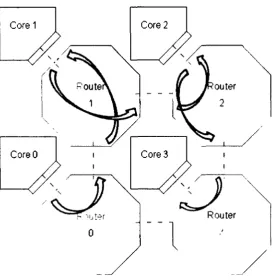
Figure 4.7: Example of a Test Scenario
Each configuration control word is 18 bits which is divided into 6 fields of 3 bits
each, depicted in Figure 4.6. Each field is designated for a partial crossbar, containing an
ID port to instruct the partial crossbar as to which input and output ports to use.
For a better understanding of how the configuration control word is determined,
an example, illustrated in Figure 4.7. is used to demonstrate this process. In this example,
data needs to be transmitted from Core 0 to Core 1. Data from Core I needs to travel to
Core 2 and data from Core 2 travels to Core 3. This example will help us show how the
configuration bit values are determined.
Table 4.3 shows the operations that are taking place in each router. A white arrow
represents the path the data needs to travel while a solid black arrow represents the
Table 4.3: Configuration Bits Value for Test Scenario
Router Scenario Configuration Bits Value
North In I Out
J:
* 5 = T ,
V
Out ' In South
i yj
rs<
• ! S
X X
K : I
•; X '55.1. | 1 j I 9 * ' III ' 1 i • a ;.3 :» ' 118 T -i 9 » •••JTf
* ^ A
1
X
I
• t !
:
X
Cri
Cse
"••J
"-%s
I
Take the first scenario; data from Core 0 needs to travel to Core 1 which has to go
through the north port. In the sub-packet for the north partial crossbar, the port ID for
core ("100") is placed while the other ports service is not needed so we placed an "X" for
don't care. Core 0 will be expecting communication signals from Core 1, so in the
reserve channel sub-packet, a port ID of "000" is placed because the communication
signals coming from Core 1 have to go through the north port.
In the second scenario, more operations are taking place. First, data coming from
Core 0 needs to go to Core I and data coming out of Core I need to travel to Core 2. A
binary representation of "010" is placed in the Core sub-packet to establish a connection
between the south input port to the core output port. Second, Core I will need to
communication with Core 0 in the south direction through the south port. Then, the core
ID is placed in the south partial crossbar sub-packet. Third, data from Core 1 need to be
route to Core 2 in an east direction. The core ID is placed in the east partial crossbar
sub-packet. Lastly, a communication channel is reserved for the east port since the
communication signals from Core 2 is coming from the east port and the rest is left
unused.
In the third scenario, incoming data from Core 1 is coming from the west port will
need to be routed to Core 2 and also data from Core 2 will need to be travel to Core 3
through the south port. Thus, west ID and core ID is placed in the core sub-packet and
south sub-packet respectively. Core 2 will be sending communication signals to Core 1,
so the core ID is place in the west sub-packet. Lastly, the reserve channel will reserved
the communication signals coming from Core 3 from the south port.
Finally, data from Core 2 comes in from the north port and the communication
signals from Core 3 will also be going through the north port. Therefore, north ID is
placed in core sub-packet and the core ID is place in the north sub-packet. This
4-2 Configuration Block
The configuration block passes the configuration information it received from the PC host
to the router. Using a handshake protocol, the PC host will signal the configuration block
for a new configuration. The configuration block recognize this by stopping all operations
by sending a low Ready signal to the router and send a request to the PC host for the
configuration bits. NoC can only resume its operation only after all routers are
configured.
From PC Host
Configuration Bits Request <— Write 1
Cros€.b:ir 2 Configuration
> 3
Configuration Bits
Ready
To Router
Figure 4.8: Crossbar Configuration Block
Table 4.4: Connection Assignment for Configuration Block
Connections Number 1 2 3 4 5 Description
Write signal from PC host to signal write operation Request signal to PC host to request a write operation Configuration Bits \ alue send by the PC host
Ready signal to signal router configuration is complete Configuration Bits value send by the configuration block
4.2.1 Primary latency
As discussed in chapter 2, the disadvantage of implementing a circuit switched protocol is
the initial latency incurred for establishing the virtual circuit. This causes the blocking of
all routers because the physical link is now reserved for setting up the new connection.
Core
Network Adaptor
Router
Figure 4.9: Block Diagram of Network Adaptor
initial latency becomes insignificant. Our proposed NoC system have nine routers that
need to be configure and the execution time to configure all nine routers is 10.8
milliseconds, at a clock speed of 50 MHz.
4.3 Network Adaptor
The task of a network adaptor is to integrate the core computational hardware block into
the NoC system. The network adaptor is responsible for communicating with the router
to receive data as input to the core and to transmit data as output from the core.
4.4 Links
Links are physical wires that transfer data from one node to another. Links are very
susceptible to the degradation of signal integrity caused by intrinsic and extrinsic noise
from the circuit, when driving the signals on a long wire. Although they may not be a
major component, links are the backbone of the infrastructure that need to be optimized
for signal integrity. Therefore, the protection of physical wires from noise and
minimizing power consumption are important design goals that should be considered at
the physical level. These issues are more important when developing NoC for ASIC
4.5 Summary
In this chapter, detailed descriptions of the functionality of each NoC blocks are given.
The implementation and functionality of the router was described and examples were
used to illustrate the operation of the router. Lastly the important functions of the
network adaptor and physical links were described. In chapter 5, the design methodology
for the proposed NoC implementation is described. We also describe the application
Chapter 5
Experimental Evaluation Framework
This chapter starts with a discussion of the design methodology for implementing an
Network-on-Chip (NoC) system. This methodology also facilitates rapid prototyping and
exploration of various aspects of NoC implementation. This is followed by a description
the Celoxica DK tool, used for NoC implementation. Then, we describe how a
Microblaze-based system is specified using the Celoxica Handel-C hardware description
language. Lastly, the applications mapping process for mapping two test applications into
the target systems, bus-based system and NoC-based system is presented.
5.1 NoC Specification and Implementation Methodology
For this research, it is important to define a framework that helps guide this research for
exploring the design space for NoC implementation. As discussed earlier in Chapter 3,
any NoC architecture implementation can be described at several layers of abstraction.
C Tmumcation Infraslnjiure
Communication Paradigm
Application Mappin g
Hard F rm
» Floor plan
1 • t
Switching Tecnniq-''
Routing Strategy
Communication & Task Scheduling
»
*
Soft
V
Topology 3 /r i-e-sts
i »r iel * ' i ! h *~ zi-i<3
Ar|p nation Mapping
Figure 5.1: Design Space for NoC Architectures [2]
5.1.1 Communication Infrastructure
Communication infrastructure determines the communication architecture for providing
optimal performance, with particular attention to design trades-offs to meet the
performance needs of the chosen application. Although customized NoC is highly
desirable for great improved performance, they bring other issues into focus such as
physical links optimization (driving uneven wire length) and low scalability (irregular
floor planning) [2]. While low complexity architecture such as the mesh can provides an
excellent platform for rapid prototyping for many applications, its performance may not
be adequate for some higher end applications. Also, communication infrastructure is
involved with network floor planning, the placement of various NoC components for
![Figure 2.4: Indirect Networks (adapted from [1])](https://thumb-us.123doks.com/thumbv2/123dok_us/1460642.1178964/24.611.140.474.70.330/figure-indirect-networks-adapted-from.webp)
![Figure 2.5: Schematic for a Generic FPGA Logic Element (LE) [14]](https://thumb-us.123doks.com/thumbv2/123dok_us/1460642.1178964/26.611.105.508.66.280/figure-schematic-for-generic-fpga-logic-element.webp)
![Figure 2.6: Schematic of a Lookup Table (LUT) [3]](https://thumb-us.123doks.com/thumbv2/123dok_us/1460642.1178964/27.614.172.443.75.293/figure-schematic-lookup-table-lut.webp)
![Figure 5 2: Design Choices for Communication Paradigm [2]](https://thumb-us.123doks.com/thumbv2/123dok_us/1460642.1178964/55.611.98.518.76.323/figure-design-choices-communication-paradigm.webp)
