ISSN (Print) : 2347 - 6710
I
nternationalJ
ournal ofI
nnovativeR
esearch inS
cience,E
ngineering andT
echnologyVolume 3, Special Issue 3, March 2014
2014 International Conference on Innovations in Engineering and Technology (ICIET’14)
On 21st & 22nd March Organized by
K.L.N. College of Engineering, Madurai, Tamil Nadu, India
ABSTRACT— This paper presents a high efficiency converter with input power source from a low voltage, high current DC source solar PV system. Therefore, it is desirable to create a power converter with a topology suited to the attributes. This converter has a coupled inductor with high transformation ratio and a voltage multiplier is adapted to step-up the input voltage with high conversion ratio. In step up mode, the primary and secondary windings of the coupled inductor are operated in parallel for charging and series for discharging to achieve high step up voltage gain. It is also proposed fuzzy logic controller (FLC) for significantly improving the performance of DC-DC converter, FLC improves the efficiency of converter by control the output voltage.
KEYWORDS— Boost converter, coupled inductor, voltage multiplier, FLC.
I. INTRODUCTION
In order to protect the natural environment on the earth, the development of clean energy without pollution has the major representative role in the last decade. By accompanying the permission of Kyoto Protocol, clean energies, such as fuel cell (FC), photovoltaic (PV), wind energy, etc., have been rapidly promote. Batteries or super capacitors are usually taken as storage mechanisms for smoothing output power, start-up transition, and various load conditions .The corresponding installed capacity of clean energies can be further reduced to save the cost of system purchasing and power supply. Solar energy is abundantly available that has made it possible to harvest it and utilize it properly.
Due to the electric characteristics of clean energies, the generated power is critically affected by the climate or has slow transient responses, and the output voltage is easily influenced by load variations.
Figure1. General block diagram of proposed system.
Solar energy can be a standalone generating unit or can be a grid connected generating unit depending on the availability of a grid nearby. Thus it can be used to power rural areas where the availability of grids is very low. Another advantage of using solar energy is the portable operation whenever necessary. The proposed dc-dc converter has an input dc-dc voltage from a solar PV systems [19].This circuit is given a closed loop through FLC from output to input by an feedback voltage with comparison of error and respective change in error from the output of the DC-DC converter [17], such that the dc-dc converter act as a boost converter which steps up the voltage from solar PV system .MOSFET switch is used due to its high switching speed and efficiency. FLC have some advantages compared to other classical controller such as simplicity of control, low cost and the possibility to design without knowing the exact mathematical model of the process. Fuzzy logic is flexible. With any given system, it is easy to layer on more functionality without starting again from scratch. Fuzzy logic is conceptually easy to understand and control the output voltage and increase the efficiency.
A converter may be designed to operate in continuous mode at high power there have been various techniques used to create high step-up converters that maintain high efficiency. Converters utilizing repeated
Solar PV
DC-DC Converter
Load
FLC Feedback
Voltage
A High Efficiency DC-DC Converter with
FLC for Solar PV
A.Ravijoney1, Mr. B.Meenakshi Sundaram
component networks, such as multiplier capacitors or voltage doublers, are described.
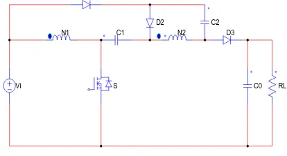
This paper presents a high efficiency Boost Converter, which uses the coupling inductor and voltage Multiplier technique .The circuit diagram of proposed converter is shown if fig.2. and the features of this converter are as follows: 1) High Efficiency 2) Duty ratio can be designed to 0.66 by adjusting the turns ratio of the coupled inductor. Thus the proposed converter can be operated under Continuous conduction mode. 3) The energy stored in the leakage inductance of the transformer is recover, thus increasing the efficiency. 4) The voltage is clamped on the switch and enabling the power switch to be selected with a low voltage rating and low conduction resistance. 5) The converter uses low –rating switch and diodes to minimize the cost.
The conventional Boost converters cannot provide such a high dc voltage gain, even for an extreme duty cycle. As a result, the conversion efficiency is degraded and the electromagnetic interference (EMI) problem is severe under this situation [1]. In order to increase the conversion efficiency and voltage gain, many modified boost converter topologies have been investigated in the past decade [4]-[14].
D1
S C1 N1
Vi
C2
C0 RL
N2 D2
D3
Figure 2.Circuit Diagram for high step-up gain converter.
II. PROPOSED CONVERTER AND OPERATION PRINCIPLE
The Fig 3 shows the circuit configuration of the proposed converter, a boost converter with a voltage multiplier and coupled inductor techniques [18]. The model of coupled inductor includes leakage inductance Lk
and a magnetizing inductance Lm and an ideal transformer.
This converter consist of a DC input supply Vi , one
coupled inductor , three diodes , one power switch and three capacitors. The most basic implementation of this principle, which is seen in[10] a Interleaved version. Which involves the capacitor is being charged by a winding of the coupled inductor when switch S is ON, and then discharging in series with both winding into the respective load such the voltage across the three components combine together to boost up the output voltage and same principle is adopted to utilize the multiple capacitors such that they charge independently at the time of switch S is ON and discharge during OFF state condition. For that the components are arranged so that during ON state, one capacitor along with the both windings discharges to another capacitor and thus boost up the output voltage even higher. During OFF state the
higher voltage capacitor can discharge, in the series with the windings into the respective load, while the other capacitor is recharged.
D1
S C1 N1
Lm
Vi
C2
C0 RL
N2 D2
D3 Lk Ii
Io
Figure 3.Equivalent circuit For Proposed Converter.
In order to realize this concept, the switch ON and OFF states of converter are treated for various arrangements of components in order to find the combination that result in desirable gain function [22]. During ON state capacitor C2 is placed in series with both
primary and secondary windings of the coupled inductor so that it discharges into and boost the voltage of C1.whereas during OFF state, C1 discharges in series with
both windings and into the load, where C2 get recharged
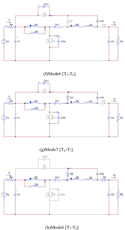
by high voltage secondary winding respectively. Here the circuit operates at four different stages according to the parameters, the main difference among the four stages are duration of conduction of three diodes D1, D2 and D3.
Stage1 is a continuous conduction mode (CCM), where switch and diode D1 conduct for a switching cycle
followed by the diode D2, D3 conducting for the
remainder. Stage 2 is same as Stage 1 except the current in D1 which reduces to zero before the switch S is turned
OFF. Stage 3 begins as Stage 1 action; where D2, D3 both
simultaneously reduced to zero before the switch S is turn ON so thus put the converter into discontinuous conduction mode (DCM).In Stage 4 all three diodes D1,
D2 and D3 reduced to zero according to their respective
operation interval. Therefore whereas Stage 1 has two main switching modes, Stage 2 and 3 have three modes, Stage 4 has four modes. This paper is focus on the main operating modes of Stage 2.
The switching modes of proposed converter as follows, the coupled inductor are modeled as an ideal transformer with magnetizing inductance and secondary series leakage inductances. The switch S and diode D1both have parasitic capacitance placed in parallel with
them. Let capacitors Ci, C0, C1 and C2 are assumed to
D1 S N1 Lm C0 RL N2 D2 D3 CDs Vi Vs Rs CD1 Lk Ii Io Vc1 Vc2
(a)Mode1[T0-T1]
D1 S N1 Lm C0 RL N2 D2 D3 CDs Vi Vs Rs CD1 Lk Ii Io Vc2 Vc1
(b)Mode2 [T1-T2]
D1 S N1 Lm C0 RL N2 D2 D3 CDs Vi Vs Rs CD1 Lk Ii Io Vc2 Vc1
(c)Mode3 [T2-T3]
D1 S N1 Lm C0 RL N2 D2 D3 CDs Vi Vs Rs CD1 Lk Ii Io Vc2 Vc1
(d)Mode4 [T3-T4]
D1 S N1 Lm C0 RL N2 D2 D3 CDs Vi Vs Rs CD1 Lk Ii Io Vc2 Vc1
(e)Mode5 [T4-T5]
D1 S N1 Lm C0 RL N2 D2 D3 CDs Vi Vs Rs CD1 Lk Ii Io Vc2 Vc1
(f)Mode6 [T5-T6]
D1 S N1 Lm C0 RL N2 D2 D3 CDs Vi Vs Rs CD1 Lk Ii Io Vc2 Vc1
(g)Mode7 [T6-T7]
D1 S N1 Lm C0 RL N2 D2 D3 CDs Vi Vs Rs CD1 Lk Ii Io Vc2 Vc1
(h)Mode8 [T7-T8]
Figure 4.Proposed converter Modes of operation for Stage 2.
(a)Mode1 [T0-T1] [see fig 4(a)]: Switch S turn ON at T0
and the capacitance CDS start discharge thro the internal
resistance of switch. Therefore D3 will stop conducting
and blocking voltage will start to rise.CD1, parasitic
capacitance will also discharge as a result voltage on CDS
dropping. Leakage inductance LK discharge through D2.
(b)Mode2 [T1-T2] [see fig 4(b)]: At T1, CDS fully
discharged. As a result, CD1 stops discharging and holds a
constant voltage for the duration of mode .LK
continuously discharges through D2.
(c)Mode3 [T2-T3] [see fig 4(c)]: At T2, LK fully
discharged and D2 gets turn OFF. Now current begins to
flow across LK in reverse direction and cause it to charge
but in reverse polarity. This reverse current also causes CD1 to discharge.
(d)Mode4 [T3-T4] [see fig 4(d)]: At T3, CD1 fully
discharged thus D1 turned ON. Then the energy is
transferred from Vi, LK C2 into Lm and C1, thus causing the
current in Lm to increase and LK to decrease. The current
slope in the L1 can either positive or negative as it is sum
(e)Mode5 [T4-T5] [see fig 4(e)]: At T4, current in leakage
inductance LK has returned to zero and D1 gets turn OFF
.Lm Continuously charges from Vi and thus, its current
increases.
(f)Mode6 [T5-T6] [see fig 4(f)]: At T5, switch S gets turn
OFF.CDS begins to charge .Thus in turn causes CD1 also
charge, as a result D2 and D3 begin to reduce. Current draw
at CD1 causes LK to charge.
(g)Mode7 [T6-T7] [see fig 4(g)]: At T6, Voltage across D2
reduces to zero and begins to conduct. The blocking D2
continues to decrease.
(h)Mode8 [T7-T8] [see fig 4(h)]: At T7, Voltage across D3
reduces to zero and begins to conduct. Lm , LK , C1
discharges their energy to C2 and to the load.
III. CONVERTER ANALYSIS A).Converter Gain:
The converter gain can be determined by modes 4,5 and 8.Where there energy transfer between the source, energy storage elements and load is shown fig 4(d),4(e) and 4(h).The voltage across Lm can be written in two ways
,from mode 4
(1)
From mode 8,
(2) Or
Similarly, equation (2) can be written as
(3)
By using voltage second balance principle on Lm of the
coupled inductor for these three stages is
(4)
By solving equations (1) – (4), the voltage gain is,
(5)
B). Efficiency analysis
The overall efficiency can be analyzed with the ratio output power and input power of the proposed converter respectively.
(6)
(7)
From the equation (6), the efficiency is calculated to be 88.2% respectively.
C). Designing of coupled inductor:
Here coupled inductor is modeled as an ideal transformer, the magnetizing inductor (Lm) and a leakage
inductor (Lk) ,the turns ratio (n) and the coupling
coefficient (k) of ideal transformer is defined
(8)
From equation (1), L1 is defined
(9)
(10)
(11)
Duty cycle is defined from the equation (5)
(12)
IV.FUZZYLOGIC CONTROLLER
Fuzzy logic starts with the concept of a fuzzy set. It can contain elements with only a partial degree of membership. A membership function is a curve that defines how each point in the input space is mapped to a membership value (or degree of membership) between 0 and 1. The input space is sometimes referred to as the universe of discourse. The degree an object belongs to a fuzzy set is denoted by a membership value between 0 and 1.
positive small, positive medium, and positive large[17]. Error and Change in error consists of these six membership functions. Output also consists of six membership function. With consideration of the inputs, output could be framed and it is controlled in it.
Figure 5. FLC simulink block.
The fuzzy logic controller block is shown in figure (5), which is implemented to stabilize the output by designing the rules in is done with the help of FAM table respectively [3].
Figure 6. Membership function plots of error.
Figure 7. Membership function plots of change error.
100 to 230
Discrete, Ts = 5e-005 s.
powergui
v + -v
+
-v +
-z 1
Out1
Temperature
Scope3
Scope2
Scope1
<= Ref Ramp
T
G +
-PV model subsystem
g
m
D
S
1 2
Fuzzy Logic Controller
Diode
i
+
-i
+
-181
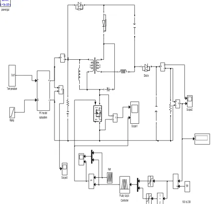
Figure 8.Simulation diagram of proposed converter.
TABLE I
FAM TABLE WITH RULES FOR ERROR AND CHANGE OF ERROR
de e
MF1 MF2 MF3
N1 P2 P1 P
N2 P3 P2 P3
N3 P1 P2 P1
N4 P5 P4 P2
N5 P6 P5 Pm8
N6 P7 P6 Pm8
N7 P1 P7 Pm8
N8 P1 Pm0 Pm3
P1 Pm2 P8 P8
P2 Pm3 Pm2 Pm8
P3 Pm4 Pm3 Pm1
P4 Pm3 Pm4 Pm1
P5 Pm6 Pm5 Pm3
P6 Pm7 Pm6 Pm5
P7 Pm8 Pm7 Pm6
P8 Pm8 Pm8 Pm7
Figure 9.Simulation result for output current.
Figure 10. Simulation result for output voltage.
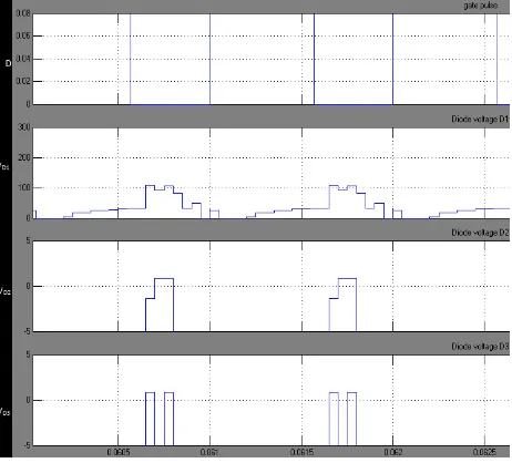
Figure 11.Simulation result of VD1,VD2 and VD3.
Thus the proposed converter high efficiency conversion is shown in the figure (10), Vo=180V, which is higher than the conventional converter.
TABLE II
PERFORMANCE COMPARISON
S.NO CONVERTERS OUTPUT
VOLTAGE EFFICIENY (%)
1 PROPOSED CONVERTER
WITH OPEN LOOP
175.5 73.7
2 PROPOSED CONVERTER WITH FLC
180.1 88.2
V. CONCLUSIONS
REFERENCES
[1] N. Mohan, T. M. Undeland, and W. P. Robbins, Power Electronics: Converters, Applications, and Design. New York:Wiley, 1995.
[2] Y. Deng, Q. Rong, W. Li, Y. Zhao, J. Shi, and X. He, “Single- switch high step-up converters with built-in transformer voltage multiplier cell,” IEEETrans. Power Electron, vol. 27, no. 8, pp. 3557–3567, Aug. 2012.
[3] K.Gopaiah,Ch.Rambabu2, “Fuzzy logic controlled bidirectional dc-dc converter applied to dc drive” IJESR/Sept 2012/Volume-2/Issue-9/Article No-38/1279-1294 ISSN 2277-2685
[4] Tsai-Fu,Yu-Sheng Lai,Jin-Chyuan Hung.and Yaow-Ming Chen,“Boost Converter With Coupled Inductors and Buck-BoostType of Active Clamp” IEEE Tran.on Industrial Electronics,VOL.55,N0.1,JANUARY 2008.
[5] Ching-Tsai Pan,and Ching-Ming Lai, “A High Efficiency High Step-Up Converter With Low Switch Stress for Fuel Cell System Application” IEEETran.on Industrial
Electronics,VOL.57,NO.6,JUNE 2010 [6] Rong-Jong Wai,and Rou-Yong Duan, “High Step-Up Converter
with Coupled Inductor” “ IEEE Trans. On Power Electron.,VOL. 20, NO. 5, SEPTEMBER 2005.
[7] Rong-Jong Wai,Chung-You Lin,Rou-Yong Duan,an Yung- Ruei Chang, “High Efficiency DC-DC Converter with High Voltage
Gain and
ReducedSwitchStress”IEEETran.onIndustrialElectronics,VOL.54, N0.1,FEBRUARY 2007
[8] Hyun-Lark Do, “A Zero-Voltage-Switching DC–DC Converter With High Voltage Gain” IEEE Trans. On Power Electron.,VOL. 26, NO. 5, MAY 2011.
[9] Yi-Ping,H,J-FChen,T-JLiang and Lung- S Yang,“A Novel High Step-Up DC–DC Converter for a Microgrid System” IEEE Trans. On Power Electron., VOL. 26, NO. 4, APRIL 2011.
[10] Hyun-Lark Do, “Nonisolated Bidirectional Zero-Voltage-Switching DC-DC Converter” IEEE Trans
PowerElectron..VOL.26,NO.9,SEPTEMBER 2011
[11] Ahmad Mousavi, Pritam Das, and Gerry Moschopoulos,“A Comparative Study of a New ZCS DC–DC Full-Bridge Boost Converter With a ZVS Active-Clamp Converter” IEEE Trans On Power Electron. VOL. 27, NO. 3, MARCH 2012..
[12] Tsai-Fu Wu, Yong-Dong Chang, Chih-Hao Chang, and Jeng- Gung Yang, “Soft-Switching Boost Converter With a Flyback Snubber for High Power Applications” IEEE Trans. OnPower Electron. VOL. 27, NO. 3 MARCH 2012.
[13] Giorgio Spiazzi, Paolo Mattavelli, and Alessandro Costabeber, “High Step-Up Ratio Flyback Converter With Active Clamp and Voltage Multiplier” IEEE Trans. On Power Electron., VOL. 26, NO. 11, NOVEMBER 2011.
[14] i-Ping Hsieh, Jiann-Fuh Chen,Tsorng-Juu (Peter) Liang, andLung-Sheng Yang, “Novel High Step-Up DC–DC ConverterWith Coupled-Inductor and Switched-Capacitor Techniques for a Sustainable Energy System” IEEE Trans. On PowerElectron. VOL. 26, NO. 12, DECEMBER 2011.
[15] F. Tofoli, D.d.s. Oliveira, R.T-Bascop´e, and Y. Alcazar,“Novel nonisolated high-voltage gain dc-dc converters based on3SSC and VMC,” IEEE Trans. PowerElectron., vol.27, no. 9, pp. 3897– 3907, Sep. 2012.
[16] R. Guo, Z. Liang, and A. Huang, “A family of multimodes charge pumpbased dc-dc converter with high efficiency wide input and outputrange,” IEEE Trans.Power Electron vol. 27, no. 11, pp. 4788–4798,Nov. 2012.
[17] B.L.Narasimharaju,SatyaPrakashDubey,S.PSingh“Performance Evaluation of Fuzzy LogicControlled Bidirectional DC to DC Converter” TECHNIA VOL. 3, NO. 2, Jan. 2011. (ISSN 0974-3375)
[18] W. Li, Y. Zhao, Y. Deng, and X. He, “Interleaved converter with voltage multiplier cell for high step-up and high-efficiency conversion,” IEEE Trans. Power Electron., vol. 25, no. 9, pp. 2397–2408, Sep. 2010.
[19] A.Pradeepkumaryadav,S.Thirumaliah,G.Haritha“Comparison of MPPT Algorithms for DC-DC Converters Based PV Systems” Vol. 1, Issue 1, July 2012.
[20] E. Carlson, K. Strunz, and B. Otis, “A 20 mV input boost converter with efficient digital control for thermoelectric energy harvesting” IEEE J.Solid-State Circuits, vol. 45, no. 4, pp. 741– 750, Apr. 2010.