A Real Time Wireless Network on Chip
Architecture with an Efficient Gals
Implementation
P.Vinothini1, Dr. K.A.Dattatreya2
PG Scholar [VLSI Design], Adhiyamaan College of Engineering, Hosur, TN, India1
Professor, Department of ECE, Adhiyamaan College of Engineering, Hosur, TN, India2
ABSTRACT: The NOC implements message passing communication through processor cores. It uses statically scheduled time-division multiplexing (TDM) to control the communication over a structure of links and network interfaces (NIs)to real-time guarantees. The area-efficient design is the result of two contributions: 1) asynchronous routers combined with TDM scheduling and 2) A novel NI micro architecture. In the result in a output in which data are transferred to the local memory of the sending core to the local memory of the receiving core, without any dynamic arbitration, buffering, andlock synchronization. In the proposed methodology wireless network on chip architecture incorporating necessary multicast Integration of WNoC (Wireless Network on Chip) architecture with Classical Bus based systems to overcome the disadvantages of both Classical and Network based methodologies. The efficiency of the proposed methodology is shown by comparing with existing method, directly into the consideration the resource requirement target is FPGA device.
I. INTRODUCTION
Design of algorithms and protocols for Network on Chip (NoC) interconnection systems investigate the following research issues: (i) Architecture analysis, intend to evaluate the main NoC architectures (ii) protocol design: investigation and proposal of novel transport and routing algorithms for the Spidergon Network on Chip. (iii) Network design: investigate the major issues in the actual NoC implementation and interconnection. The analysis and the characterization of protocols and architectures for NoC systems they propose throughout thesis have been obtained towards computer-based simulation. According to the International Technology Roadmap for decade complex systems, called Multi Processor System-on Chip (MPSoC), will contain billions of transistors running at a frequency of many Giga Hz.
The technology of semiconductors keeps on scaling down allowing more and more components to be installed within the same area of a chip. As a consequence complex systems that once required many microchips for being built, now can be fixed on a single microchip containing all the system and the interconnection channels connecting them. Examples of these capabilities are the recent eight-cores IBM’s Cell processor installed on the Sony’s Playstation III and the more futuristic eighty cores Intel’s Teraflop processors.
II. RELATED WORK
MPSOC (MULTIPROCESSOR SYSTEM ON CHIP)
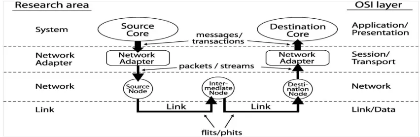
A central and key element in future complex MPSoC is the global On–chip Communication Architecture (OCCA) or On Chip Interconnect (OCIN): the infrastructure that interconnects the components of a MPSoC and provides the means necessary for distributed computation among different processing elements. The natural evolution of the bus-based solution reported and the poorly scalable point to point networks are the new generation architectures called Network on-Chip (NoC) represented NoC are packet-switched communication networks derived from the parallel computing domain. They are based on a well-defined protocol stack same to the ISO/OSI seen in the network on computers. A layered-stack approach to the design of the on-chip inter-core communications can be defined accordingly with the communication-based methodology that community, the global on-chip communication is decomposed into layers similar to the ISO-OSI Reference Model. The protocol stack enables different services, providing to the programmer an abstraction of the communication framework. Layers through well-defined interfaces and they hide the low level.
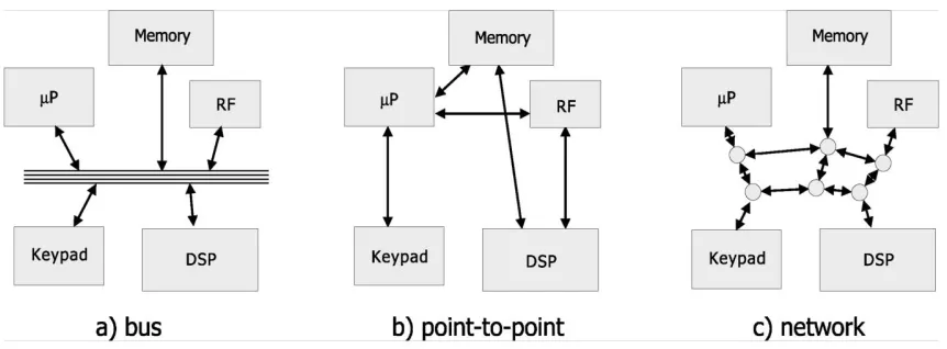
Fig 2: Examples of communication structures in Systems-on-Chip
• Network level: handles issues related to the topology and the consequent routing scheme. • Transport layer manages the end-to-end services and the packet segmentation/reassembly.
Upper levels can be viewed merged up to the Application as a sort of adaptation layer that implements (in HW or through part of an OS) services and ISO-OSI Reference Model exposes the NoC infrastructure according to a Message Passing (MP) programming paradigm. Despite the similarity discussed above, it is clear that the micro-network in the single chip domain differs from the wide-area micro-networks under many different aspects.
ISO-OSI REFERENCE MODEL
or battery-powered systems. Controlling and minimizing the need of power is a vital aspect especially for portable systems such as phones and multimedia devices that will heavily relay on NoC interconnects; need of low cost and low complexity solutions: NoC interconnects will be extensively used in many commercial-oriented electronic devices.
The minimization of costs of all sort is an important aspect of for the development of these systems; reusability: by providing standard Network Interfaces the same network cabe used to interconnect heterogeneous components that implement different tasks or algorithms and that are designed by third party companies.
CHIP MULTI PROCESSOR
(CMP) are networks designed to support any kindof traffic. At the network’s design time no knowledge about the traffic is available. CMP hence are built to offer best effort services. Quality of services (QoSs) capabilities can be granted by differentiating the traffic into classes of priorities each one assigned to a specific virtual channel (VC) or by providing guaranteed service levels on dedicated connection. CMP systems are mainly composed by similar components grouped such as sets of processors and memories. This allows the use of regular topologies often borrowed from the parallel computing world such as 2D Mesh, Torus, Ring etc...
SYSTEM ON CHIP
(SoC) are systems integrating heterogeneous components, often developed by third party companies at the purpose of building an application specific systems. In SoC often the traffic patterns are known since the design time hence the interconnection networks can be built to exactly match the application requirement. In SoC for embedded applications designers use standard industrial CAD-tool flows for the synthesis of a platform-specific NoC and must cope with an increasing
Fig 3: ISO-OSI Reference Model
III. EXISTING SYSTEM
schedule, such that each channel has one bandwidth guarantees. DMA transfers have to be interleaved correspondingly, with one DMA controller per outgoing channel. On the other hand, the NI can only inject one packet at a time into the NoC, Fig. Block diagram showing the micro architecture of the Argo asynchronous router and the packet format. For clarity, the request and acknowledge handshake signals are not shown. And consequently, only one DMA controller can be active at a time. This allows a single table-based implementation of all the DMA controllers, where each entry of the table refers to one DMA controller, i.e., one outgoing channel. In addition, the dual-ported SPMs can be used for clock domain crossing. In this way, explicit clock domain crossings are needed only to program the DMA controllers; the actual transfer of message data does not require any synchronization.
The combination of interleaved DMAs and dual-ported SPMs creates a direct path from the SPM to the network of routers, avoiding the need for flow control and buffering in the NIs as well as latency for clock domain crossing for the message data. Flow control between NIs can be omitted, since the receiving SPMs always accept incoming transactions, i.e., offer a consumption guaranteed data are transferred from the source SPM across the NoC and intothe destination SPM without any buffering, flow control, or clock domain crossings. The result is a very small and efficient NI implementation. Since NIs has the responsibility of enforcing the TDM schedule, we have chosen a clocked implementation. In contrast to an asynchronous implementation, a clocked one simplifies the synthesis process and the task of evaluating WCETs.
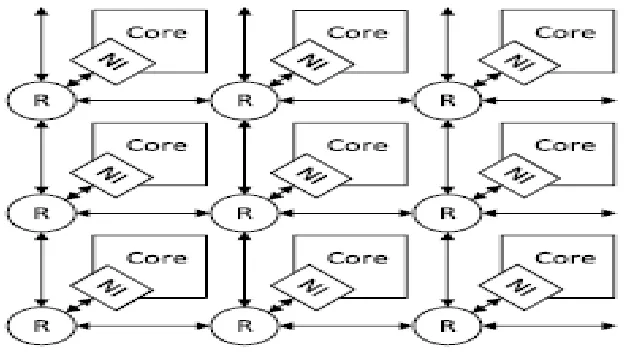
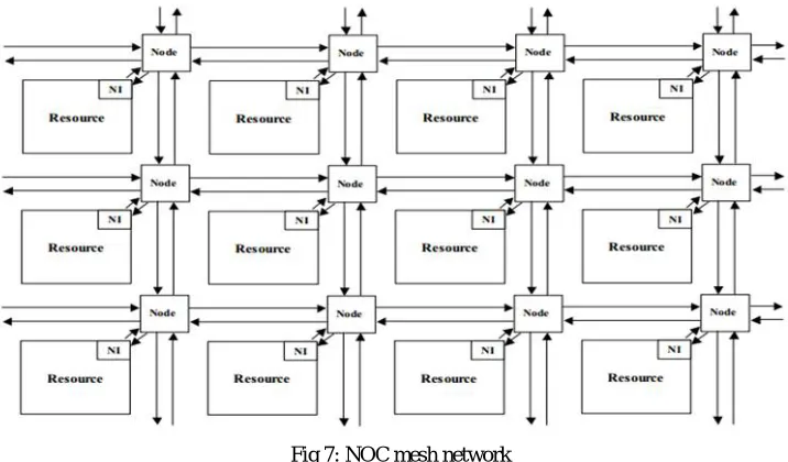
Fig 4: multiprocessor 2-D mesh NoC topology
ASYNCHRONOUSARGOROUTER
Fig 5: A Processor wireless Noc
The router is a three-stage pipeline: 1) link traversal; 2) header parsing unit (HPU); and 3) traversal of theXbar switch. A router typically has five ports, and this allows the construction of mesh-type topologies.
Fig 6: Existing system topology
DISADVANTAGES
IV. PROPOSED SYSTEM
In this proposed methodology NOC architecture for classical bus based systems to overcome the limitations of GALS implementation by reducing routers and network interfaces.
In this proposed method only 2 routers and 2 network interfaces are used to give less area, power and fast latency.
ADVANTAGES
The proposed classical bus based NoC architecture design will make less area when compared to the existing GALS architecture which occupies less digital components.
The less no of digital components makes the gate-level counts in less number, which leads to increase the speed of the circuit and consumes less amount of power in the soc level integration.
V. LITERATURE SURVEY
An Asynchronous NOC Architecture Providing Low LatencyService and its Multi-level Design Framework.
such as bus hierarchy, point-to-point links, crossbars, still face the same issues: difficulties in timing validation and in connecting blocks running at different speeds, limited throughput versus power efficiency. Since three years, the term “Network-on-Chip” (NOC) has appeared.
The advantages of a NOC based architecture are numerous: high scalability and versatility, high throughput with good power efficiency. For very large scale integration, NOC are fully scalable, because the number of nodes can be increased to provide higher global throughput, without degrading local network linkperformances. NOC based architecture and packet switching provide dynamic communication possibilities, which lead to versatility. At chip level, the longest wires are only connected to two nodes which is good for localthroughput. Finally, data communication and its associated power consumption can be reduced to only active network links. NOC protocols are commonly based on packet switching and cannot easily guarantee low latency.
Some NOC architectures based on “Quality of Service” have been proposed to solve communication latency and real time constraints.If previous inherent NOC properties solve most of current bus-based limitations, clock management ofaNOC-based chip is still an issue when multi-clock synchronization is required. These NOC architectures should be implemented using Globally AsynchronousLocally Synchronous techniques (GALS), since interfacing synchronous and self-timed circuits is known to be feasible. Delay Insensitive (DI) asynchronous communication will moreover provide chip level communication robustness, ensuring functionality in a large voltage and process range. With DI encoding, delay variations, due to physical constraints such as crosstalk, are no longer an issue. Wire pipelining is easy to achieve at chip level by adding asynchronous latches, in order to re-power the signals while cutting-off the wire cycle time.Some asynchronous packet-switching interconnects have been previously proposed to address synchronous implementation issues. In a Delay Insensitive asynchronous interconnect using one-hot DI data encoding provides robustness.
Fig 7: NOC mesh network
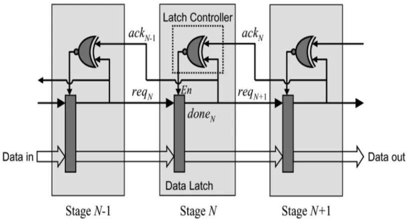
MOUSETRAP: HIGH-SPEED TRANSITION-SIGNALING ASYNCHRONOUS PIPELINES
Montek Singh and Steven M. Nowick
synchronous designers are currently capable of achieving multi-gigahertz clock distributions,the task involves the ever-increasing challenges of design time, verification effort, clock skew, and power management, and interfacing with different timing domains. Second, since an asynchronous pipeline has no global clock, it has a natural elasticity: the number of data items in the pipeline, and the speeds of the external interfaces, can vary dynamically. As a result, the pipeline can gracefully interface with environments operating at different rates, including those subject to dynamic voltage scaling, thus facilitating modular and reusable design. Finally, the localized control of asynchronous pipelines is an excellent match for very high throughput fine-grain data path. The new pipeline is characterized by the simplicity of its structure and operation, as well as by ease of design. The data path uses standard transparent latches which are small and fast, and, for a basic linear pipeline, the asynchronous control consists of only a single gate per pipeline stage. Pipeline stages communicate only with immediate neighbour stages, and the timing constraints are all local, simple, and one-sided. While the proposed pipeline style has general applicability, a special focus of this paper is to target extremely high throughput. In particular, fine-grain, or “gate-level,” pipelines are proposed, where the function logic in each stage is only one gate deep. In each case, a new, highly-concurrent protocol is used; as a result, a basic MOUSETRAP pipeline without logic has a cycle time of only 5–6 CMOS gate delays (three components).
When a pipeline stage is waiting for data, its latch remains transparent; as soon as data enters the stage, it is captured by closing the latch behind it. While there have been other asynchronous pipelines that have used this kind of latching action each has its own limitations. In effect, our goal in this paper has been to build a “better mousetrap.” Post-layout simulations using SPICE are quite encouraging: a 2.10–2.38 GHz1 throughput in a TSMC 0.18- m process. The paper is organized as follows. Section II introduces the new pipeline, including its structure and operation, some performance-oriented optimizations, and extensions to handle forks and joins. Section III presents previous work on synchronous 1Strictly speaking, when referring to the throughput of asynchronous designs, the unit “gigahertz” should actually be interpreted as
APPLICATIONOF NETWORKCALCULUS TO GUARANTEED SERVICE NETWORKS
Jean-Yves Le Boudec, Member, IEEE
They call network calculus a set of rules and results that can be used for computing tight bounds on delays, backlogs, and arrival envelopes in a lossless setting applicable to packet networks. Fundamental work has been pioneered by Parekh and Gallagher and Cruz, where general bounds based on the concepts of arrival and service curves are derived. Other fundamental work for specific or general scheduling policies is described .Recently; this work has been extended and simplified independently and simultaneously under equivalent forms by Saroyan who gives a formal and general treatment of the concepts of arrival and service curves, two fundamental network calculus tools. The mathematics involved in network calculus uses min-plus algebra, as described. In this paper, we show how these results can be applied to derive general concepts for packetnetworks with guaranteed service.
They also provide a simple proof that shaping a traffic stream to conform with a burrstones constraint preserves the original constraints satisfied by the traffic stream. The Internet Engineering Task Force (IETF) is developing a framework for packet networks offering guaranteed quality of service. We show how the network calculus results mentioned above can be applied to derive general concepts for packet networks with guaranteed service. First, in Section IV, we show how rate-based schedulers can be modeled simply in a way that fits with the IETF framework. Secondly, in Section V, we introduce the general concept of deterministic effective bandwidth, which was introduced in a narrower context. We give a simple, general definition, and show that it is a convex function of the arrival curve. We also define similarly the deterministic equivalent capacity, by analogy to the work Third, and this was our initial motivation, we consider a connection admission control (CAC) method, for the case where connections are admitted onto an Asynchronous Transfer Mode (ATM) variable bit rate (VBR) trunk, or tunnel.
Fig 9: Input and output functions for GR scheduling
VI. EXPERIMENTAL RESULT
MASTER
SLAVE 11 - SIMULATION OUTPUT
SLAVE 01 - SIMULATION OUTPUT
IV.CONCLUSION AND FUTURE SCOPE
The proposed integrated NoC architecture design will make less area when compared to the existing network bus architecture which occupies less digital components. The less no of digital components makes the gate-level counts in less number, which leads to increase the speed of the circuit and consumes less amount of power in the soc level intregration. GALS based NOC architecture have been studied with literature papers. In Existing system number of routers and network interface cards are high to transfer data’s between ip cores.Master output is discussed here. Reduced NI’s & Routers will be discussed in Phase 2.
REFERENCES
[1] W. J. Dally and B. Towles, “Route packets, not wires: On-chip interconnection networks,” in Proc. Design Autom. Conf., Jun. 2001, pp. 684–689.
[2] L. Benini and G. De Micheli, “Networks on chips: A new SoC paradigm,” Computer, vol. 35, no. 1, pp. 70–78, Jan. 2002. This article has been accepted for inclusion in a future issue of this journal. Content is final as presented, with the exception of pagination. KASAPAKI et al.: ARGO: REAL-TIME NoC ARCHITECTURE WITH AN EFFICIENT GALS IMPLEMENTATION 13
[3] F. Clermidy et al., “A 477 mWNoC-based digital baseband for MIMO 4G SDR,” in IEEE Int. Solid-State Circuits Conf. Dig. Tech. Papers, Feb. 2010, pp. 278–279.
[4] J. Howard et al., “A 48-core IA-32 processor in 45 nm CMOS using on-die message-passing and DVFS for performance and power scaling,” IEEE J. Solid-State Circuits, vol. 46, no. 1, pp. 173–183, Jan. 2011.
[5] L. A. Plana et al., “SpiNNaker: Design and implementation of a GALS multicore system-on-chip,” ACM J. Emerg. Technol. Comput. Syst., vol. 7, no. 4, 2011, Art. ID 17.
[6] L. Benini, E. Flamand, D. Fuin, and D. Melpignano, “P2012: Building an ecosystem for a scalable, modular and high-efficiency embedded computing accelerator,” in Proc. Design, Autom. Test Eur. (DATE),Mar. 2012, pp. 983–987.