Modeling and Optimization Techniques
of Electronic Devices Using Genetic
Algorithm
Sherif Michael
Department of Electrical and Computer Engineering, Naval Postgraduate School, Monterey, California, USA
A new method for developing a realistic physical model of any type of solid state device is presented. Application to model advanced multi-junction solar cells; Thermo-photovoltaics; sensors; as well as other novel solid state devices are introduced in this presentation. The primary goal of multijunction solar cell design is to maximize the output power for a given solar spectrum[1-4]. The construction of multijunction cells places the individual junction layers in series, thereby limiting the overall output current to that of the junction layer producing the lowest current [5-7]. The solution to optimizing a multijunction design involves both the design of individ-ual junction layers which produce an optimum output power and the design of a series-stacked configuration of these junction layers which yields the highest possible overall output current. This paper demonstrates the use of Genetic Algorithm in a two-part process to refine a given multijunction solar cell design for near-optimal output power for a desired light spectrum. This approach can similarly be utilized to optimize the parameters of any Solid state device to yield any desired performance.
Keywords: modeling, solar cells, photovoltaics, opti-mizations, genetic algorithm
1. Introduction
The optimization routines described in this pa-per use a solar cell model developed earlier at the Naval Postgraduate School(NPS)using the ATLAS device simulator by SILVACO Interna-tional [8]. This model accurately predicts the electrical characteristics of a solar cell based on virtual fabrication of its physical structure. As an example, an InGaP/GaAs/Ge triple-jun-ction solar cell is modeled, and the device light-induced photogeneration, along with the corre-sponding spectral response of each layer, are illustrated in Figures 1 and 2.
Figure 1.ATLAS photogeneration rate output for a multi-junction solar cell for different light wavelengths.
Figure 2.Spectral response of the individual cells
(dashed)and of the stacked cell(continuous).
2. The Genetic Search Algorithm
The first step in the optimization process is to maximize the output power of each junction layer individually for several layer thicknesses. These optimum configurations will be used to ensure maximum junction layer output power as junction layer thicknesses are changed dur-ing the current-matchdur-ing process. The junction layer optimization process accepts known ma-terials for the window, emitter, base and back surface field (BSF) and determines the ideal thicknesses and doping levels for each region. The base thickness was chosen to be a depen-dent variable to achieve a constant overall junc-tion layer thickness. Thus, seven independent variables remain for each overall junction layer thickness. To search all possible solutions rig-orously would require an enormous amount of computational time.
Instead, a genetic algorithm [11] was used to search the solution space for the junction layer configuration producing the highest output power.
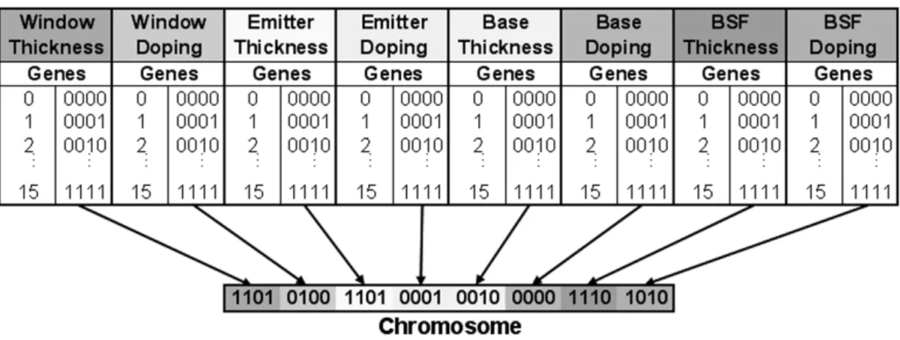
To enact a genetic algorithm for junction layer optimization, each of the eight variable junc-tion layer parameters was encoded into a four-bit binary string. The encoded binary strings, referred to as genes, were then assembled into 32-bit binary chromosomes.
Figure 3 illustrates the construction of 32-bit bi-nary chromosome from a gene sequence. Each chromosome fully encoded the eight variable properties of a junction layer. A set of 35
ran-domly selected binary strings made up the ini-tial generation of chromosomes. The encoded properties in each of these chromosomes were used to construct and simulate a junction layer ATLAS under AM0 illumination. After the sim-ulation of an entire generation of chromosomes, child chromosomes (to make up the next gen-eration)were formed from a mix of the genes from the best performing parent chromosomes. In addition, the best performing chromosome of each generation was passed unchanged into the next generation.
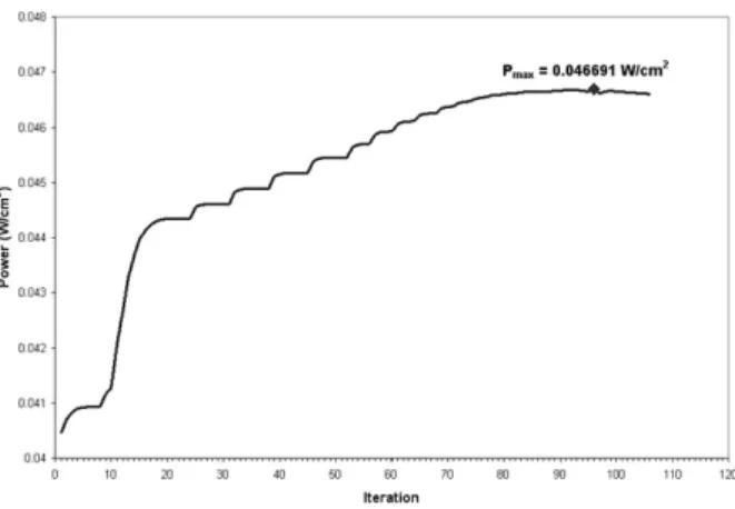
The genetic search algorithm was allowed to progress for a maximum of 20 generations. This scheme allowed a solution space of over 268 million junction layer designs to be searched to arrive near an optimal junction layer configura-tion for a specific thickness. Figure 4 demon-strate the improvement in the cell output power.
Figure 4.Improving the GaAs junction layer output power.
3. Iterative Current Matching Routine
To achieve a maximum overall output current from the full multijunction cell, the current produced by each junction layer needed to be matched to the fullest extent possible. To ac-complish this, we used an iterative current-matching routine beginning with an ATLAS simulation of the full multijunction cell with each junction layer thickness larger than its es-timated final thickness. In this initial state, each junction layer absorbed a large amount of light and little light energy was able to penetrate to each lower junction layer successively.
To match short-circuit currents, junction layers were grouped into pairs from the top junction to the substrate junction(Figure 5). Short-circuit currents were matched within the pairs by ei-ther increasing or decreasing the thickness of the upper junction layer.
Figure 5.Progress of iterative current matching routine.
Then the junction layers were re-grouped with the other adjacent junction layer and the process repeated iteratively until the short-circuit cur-rents of all junction layers were within 99.6% of each other. At this point, the routine changed focus to attempt to match the maximum-power currents of the individual junction layers. The routine ceased when all junction layer maxi-mum-power currents were matched. The op-timum cell configuration could then be deter-mined by a review of the output file for the cell with the highest overall maximum power( Fig-ures 6 and 7).
Figure 6.Optimum triple-junction cell output power.
Figure 7.Optimum quad-junction cell output power.
It was necessary to ensure that each junction layer performed optimally at each of the many thicknesses used in the iterative current-match-ing routine. This was accomplished by us-ing the optimized parameters from the genetic search algorithm for each junction layer. When a junction layer thickness was required that had not been specifically solved for during junc-tion layer optimizajunc-tion, interpolajunc-tion between known optimum values was used.
4. Results
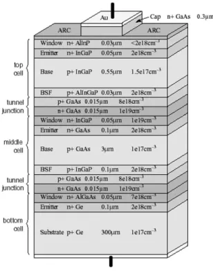
Figure 8.The new optimized triple-junction cell structure.
Figure 9.I-V curve for optimized 3-junction.
Figure 10. I-V curve for optimized 4-junction.
The advantage of this technique is therefore demonstrated using unpublished three- and four-junction solar cell designs that have been real-ized using ATLAS. Figures 8 and 9 illustrate the optimized triple-junction cell structure and itsI−V output.
Characteristics of the novel optimized quad-junctionI−Vare presented in Figure 10, which clearly shows the unprecedented output power achieved using these optimization efforts. The successful efforts presented here using ad-vanced multi-junction solar cell designs, which achieved devices with record conversion effi-ciencies, can be similarly used to optimize many solid state devices at a very moderate cost.
References
[1] R. R. KING, N. H. KARAM, J. H. ERMER, N. HAD -DAD, P. COLTER, T. ISSHIKI, H. YOON, H. L. COTAL, D. E. JOSLIN, D. D. KRUT, R. SUDHARSANAN, K.
EDMONDSON, B. T. CAVICCHI ANDD. R. LILLING -TON, “Next-generation, high-efficiency III-V
mul-tijunction solar cells”, Proc.Twenty-Eighth IEEE Photovoltaic Specialists Conference, pp. 998–1001, 2000.
[2] T. AGUI, T. TAKAMOTO, E. IKEDA, H. KURITA,
“High-efficient dual-junction InGaP/GaAs solar cells with improved tunnel interconnect”, Proceed-ings of the International Conference on Indium Phosphide and Related Materials, pp. 203–206, 1998.
[3] S. KURTZ, J. F. GEISZ, D. J. FRIEDMAN, J. M. OLSON,
A. DUDA, N. H. KARAM, R. R. KING, J. H. ERMER ANDD. E. JOSLIN, “Modeling of electron diffusion
length in GaInAsN solar cells”,Conf. Record of the Twentyeighth IEEE Photovoltaic Specialists Con-ference, pp. 1210–1213, IEEE Press, New York, 2000.
[4] I. VURGAFTMAN, J. R. MEYER AND L. R. RAM
-MOHAN,, “Band parameters for III–V compound
semiconductors and their alloys”, Applied Physics Review, J. of Applied Physics, Vol. 89, No. 11, pp. 5815–5875, 1 June 2001.
[5] KINSEY, G. S., KING, R. R., EDMONDSON, K.
M., STAVRIDES, A. P., YOON, H., FETZER, C. M.,
COLTER, P. C., ERMER, J. H., GILLANDERS, M. S.,
HEBERT, P., GRANATA, J. E. ANDKARAM, N. H., "Ultra Triple-junction High-efficiency Solar Cells",
IEEE AESS Systems Magazine, pp. 8–10, March 2003.
[6] N. H. KARAM, R. R. KING, M. HADDAD, J. H. ER -MER, H. YOON, H. L. COTAL, R. SUDHARSANAN, J.
W. ELDREDGE, K. EDMONDSON, D. E. JOSLIN, D. D. KRUT, M. TAKAHASHI, W. NISHIKAWA, M. GILLAN
in high-efficiency Ga0.5In0.5/GaAs/Ge dual- and triple-junction solar cells: steps to next-generation PV cells,” Solar Energy Materials & Solar Cells, Vol. 66, pp. 453–466, 2001.
[7] H. L. COTAL, D. R. LILLINGTON, J. H. ERMER, R. R.
KING, N. H. KARAM, S. R. KURTZ, D. J. FRIEDMAN,
J. M. OLSEN, J. S. WARD, A. DUDA, K. A. EMERY ANDT. MORIARTY,, “Triple-junction Solar Cell Effi-ciencies Above 32%: The Promise and Challenges of Their Application in High-Concentration-Ratio PV Systems”, Conf. Record of the Twentyeighth IEEE Photovoltaic Specialists Conference, pp. 955– 960, IEEE Press, New York, 2000.
[8] ATLAS User’s Manual, Vols. 1-2, software ver-sion 5.6.0.R, Silvaco International, Sunnyvale, CA, 2003.
[9] S. MICHAEL AND P. MICHALOPOULOS. “A New
Technique for the Development of State-of-the-Art Photovoltaic Devices using Silvaco Software,” Proceedings of the6th WSEAS International Mul-ticonference on Circuits, Systems, Communications and Computers(CSCC 2002), Crete, Greece, July 7-14, 2002. pp. 4121–4125.
[10] S. MICHAEL, A. BATES ANDM. GREEN, “SILVACO
ATLAS as a Solar Cell Modeling Tool,” Proceedings of the 31st IEEE Photovoltaic Specialists
Confer-ence, Jan. 3–7, 2005, Orlando, FL, pp. 719–721.
[11] K. F. MAN, K. S. TANG ANDS. KWONG, “Genetic
Algorithms: Concepts and Applications”, IEEE Transactions on Industrial Electronics, Vol. 43, No. 5, pp. 519–534, 1996.
Received:June, 2008
Accepted:September, 2008
Contact address:
Sherif Michael Department of Elec. & Comp. Engr. Space Systems Academic Group Naval Postgraduate School Monterey, CA 93943, USA e-mail:[email protected]
SHERIFMICHAEL(IEEE: S’78-M’83-SM’89)received his B.S.E.E. in
1974, the M.S.I.E. & Ph.D. degrees in 1980 and 1983, respectively, from West Virginia University, Morgantown, WV. He joined the De-partment of Electrical and Computer Engineering at the Naval Post-graduate School, Monterey CA, in 1983, where he is now a Professor. He is also one of the founding members of the Space System Academic Group since its initiation in 1985. His present research interests are in the following areas: modeling design and optimization of multi-junction solar cells; radiation and space effects on photovoltaic devices, multi-junction, gallium arsenide(GaAs)and indium phosphide(InP)
solar cells, and spacecraft power system design; radiation effects on hardened, mil. spec. devices and design of radiation tolerant ASIC; gallium arsenide(GaAs)and BiCMOS VLSI design; analog circuits design; high speed, high accuracy op amps and applications in A/D. converters; digitally controlled programmable active filters; signal pro-cessing: switched capacitor filters; minority carrier and laser annealing of GaAs and InP solar cells; digital circuit design and microprocessor applications.
In over 25 years as a faculty member at NPS, he has served as thesis advisor for more than 90 ECE/Space students. He has more than 100 technical publications in professional journals and international confer-ence proceedings. He organized and chaired the 1998 IEEE Interna-tional Symposium on Circuits and Systems, in Monterey, CA. He also organized and chaired the 34thMidwest Symposium on Circuits and