Study of Structural, Morphological and Electrical
Properties of WO
3Thin Films by e-beam Technique
Madhukar P1, Shanmukhi Jyothi D.2, Jayababu N.3 and Ramana Reddy M.V.4
1,3,4Thin Films laboratory, Department of Physics,
Osmania University. Hyderabad, INDIA 2Associate Professor of Physics,
Sardar Patel College, Secunderabad, INDIA.
(Received on: October 29, Accepted: November 8, 2017)
ABSTRACT
Amid transition metal oxides, tungsten trioxide (WO3) is one of the utmost
stimulating material exhibiting a wide range of novel properties predominantly in thin film form.The paper studies the variations on structural and dielectric properties of WO3 thin films deposited by using e-beam technique.The WO3 films were annealed
at the temperatures 400oC-600oC which represented the orthorhombic phase of
WO3.Structural properties of as deposited and annealed WO3 thin films were
characterized by XRD. The micro structural and compositional studies were performed by SEM and EDAX respectively. DC resistivity measurements were taken using Keitheley 2000 source meter.
Keywords: Structure, Morphology, WO3, Thin films, dielectric constant.
1. INTRODUCTION
temperature on the structural and dielectric properties of WO3 thin films prepared by electron beam evaporation technique.
2. EXPERIMENTAL
The WO3 powder of purity 99.999% was procured from Sigma Aldrich. Commercially available quartz glass slides were washed using detergent and deionized water followed by ultrasonic bath for 15 minutes and dried in argon gas atmosphere. The WO3thin films of thickness 200 nm were deposited onto the substrates employing electron beam evaporation technique at a substrate temperature of 200oC. Total pressure in the chamber was kept at 2X10 -5mbar and the distance between source and substrate was 12 cm. These deposited WO
3 thin films were subjected to air annealing at temperatures 400oC, 500oC and 600oC for one hour in a furnace.
The structural properties of as deposited and annealed WO3 thin films were characterized employing Grazing Incidence X-ray diffractometer using CuKα (λ=1.54 𝑨̇) in the 2Ѳ range from 20o to 70o. The micro structural and compositional studies were performed by SEM and EDAX respectively. DC resistivity measurements were taken using Keitheley 2000 source meter.
3. RESULTS AND DISCUSSIONS
3.1 Structural Studies of WO3 Thin Films by XRD
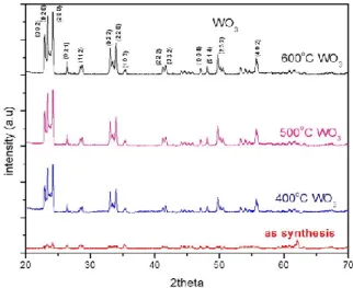
The structure of WO3 films was analyzed using a Grazing Incidence X-ray diffractometer with Cu Kα (λ = 1.5418 Ao) target. The X-ray diffraction profiles were recorded in the scanning angle range20o – 70o with a scanning speed of 1 deg /min. The X-ray diffraction spectra of as deposited and annealed WO3thin films are shown in Figure 1, which are consistent with the values in the standard card (JCPDS 71-0131).The WO3 films annealed at the temperatures 400oC-600oC showed characteristic (020), (021), (002) orientations representing the orthorhombic phase of WO3.
The average size of the crystalline grains of the samples was calculated using Debye Scherrer formula given by:
Dhkl= 0.89λ
βcosθ (1)
Figure 1: XRD patterns of as deposited and annealed WO3 thin films.
Table.1. Average grain size and strain of as prepapred and annealed WO3 thin flims from XRD.
S.No Annealing temperature(oC) Average grain size(nm) Strain ɛ(%)
1 400 40.32 1.7
2 500 51.93 2.9
3 600 56.19 15.4
3.2 Scanning Electron Microscopy (SEM), and Energy Dispersive X-Ray (EDX) of Thin Films
Figure 2.displays the surface SEM images of the as deposited and annealed thin films. All the sample films are very compact. The sizes of the electron beam evaporated tungsten oxide grains look very uniform and are a little less than 100 nm. The grain boundaries become more and more discernable after annealing at the temperature of 500oC and become very indistinct owing to the growth of the grains after post deposition heat treatment. This process indicates the structure transformation of the sample films from the complete amorphous nature to crystallization and is in complete agreement with the results confirmed by XRD (Figure 1). The surfaces of the deposited films become rougher as the annealing temperatures rise.
It is well known that during the deposition of thin films by electron beam evaporation method, a large number of oxygen vacancies and defects, which can reduce the tungsten ions from W6+ to W5+ or W4+, would be produced in the deposited films. This is responsible for the amorphous nature of the as deposited WO3 films.
Figure 2: SEM images of WO3 thin films A)& C) As deposited, B)&D) Annealed at 500oC
Figure 3: EDAX spectra ofWO3 thin films A) As deposited and B) Annealed at 500oC
the real part of the dielectric constant. The complex dielectric constant εc is given by the relation:
εc = εr +εi = (n+ik)2 (5)
Where real part εris the normal dielectric constant, and imaginary part εi represents the absorption associated with free carriers. The spectral variation of the real and imaginary part of the dielectric constant for the films annealed at 500oC and 600oCis shown in Figure4 and Figure5 respectively. The behavior of both the plots are same, but the values are different for the films annealed at 500oc and 600oc.
3.3 Dielectric Properties
To determine the effect of temperature and frequency on impedance, dielectric constant, dielectric loss and AC conductivity, frequency dependent impedance spectroscopy measurements were carried out at different temperatures. The value of dielectric constant (ε’) was calculated using the formula:
ε′=Cp X d
ε0A (6)
Where εo is the permittivity of free space, d is the thickness of thin film, A is the cross sectional area of the flat surface of the thin film and Cp is the capacitance of the specimen in Farad (F).
Figure 4: Wavelength dependence of real and imaginary parts of dielectric constant of WO3 thin films
Figure 5: Wavelength dependence of real and imaginary parts of dielectric constant of WO3 thin films
annealed at 600oC
The complex dielectric constant ε11 of the samples was calculated using the relation
𝜀′′ =ε′tanδ (7)
Where tanδ is the dielectric loss tangent which is proportional to the loss of energy from the applied field into the sample (this energy is dissipated as heat) and therefore denoted as dielectric loss. The AC conductivity of the samples was determined using the relation: 𝜎𝑎𝑐= 𝜀′εoωtanδ (8) Where ω is the angular frequency.
Figure 6. Shows the variation of dielectric constant of WO3 thin films as a function frequency at different temperatures. It was observed that dielectric constant decreases with increase in frequency for all the temperatures. The dielectric constant decreases with frequencies and remains nearly constant at higher frequencies, showing the dispersion of dielectric constant at lower frequencies. Decrease in dielectric constant takes place when jumping frequency of electric charge cannot follow the alternations of applied electric field beyond a certain critical frequency. At higher frequencies, the losses are reduced and the dipoles contribute to the polarization. The large value of dielectric constant is associated with space charge polarization and in homogeneities like voids due to wire-like structure.
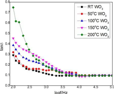
Loss factor (tanδ=ε11/ε 1) which means the phase difference due to the loss of energy within the sample at a particular frequency, is shown in Figure 7. If the electric polarization in a dielectric is unable to follow the varying electric field, dielectric loss occurs. This dependency can be explained as the average time spent by the carrier traps and depends on the energy difference between the two states. An applied field will alter this energy difference and will therefore produce a net polarization, which lags behind the applied field because the tunneling transition rates are finite. This part of the polarization, which is not in phase with the applied field, is termed as dielectric loss of the AC conductivity.
Figure 7. Variation of dielectric loss of WO3 thin film with frequency at different temperatures
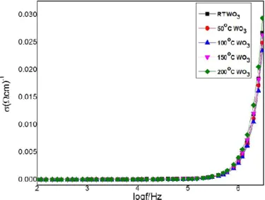
Figure 8. Variation of AC conductivity with frequency for WO3 thin films at different temperatures
Figure 8.Shows the variation of AC conductivity of WO3 thin film as a function of frequencies at various temperatures. It is evident that the AC conductivity increases with the increase in frequency, indicating the mobility of charge carriers responsible for hopping. As the frequency increases, mobility of hopping ions increases, causing an increase in the conductivity. AC conductivity increases with increase in temperature, indicating the mobility of charge carriers responsible for hopping. As the temperature increases, the mobility of hopping ions increases, causing an increase in conductivity.
CONCLUSIONS
The investigations so far carried out by us show that WO3 thin films prepared by physical vapour deposition method using e-beam present good adhesion to glass at a substrate temperature of 2000C. Post growth annealed samples have been characterized by XRD, SEM, EDAX. The XRD results show that there is an increase in grain size with temperature which can be attributed to atomic diffusion. EDAX results show that there is perfect stoichiometry of WO3. The dielectric constant decreases with frequencies and remains nearly constant at higher frequencies. At these frequencies the losses are reduced and the dipoles contribute to polarization.
ACKNOWLEDGMENTS
REFERENCES
1. Manno D, Serra A, Di Giulio M, Micocci G, Tepore A., Physical and structural characterization of tungsten oxide thin films for NO gas detection, Thin Solid Films
324:44-51; (1998).
2. Sivakumar R, Gopalakrishnan R, Jayachandran M, Sanjeeviraja C. Preparation and characterization of electron beam evaporated WO3 thin films. Opt Mater (Amst) 29:679-87; (2007).
3. Liu X, Wang F, Wang Q. Nanostructure-based WO3 photoanodes for photo-electrochemical water splitting. Chem Phys 14:7894-911; (2012).
4. Wei S, Ma Y, Chen Y, Liu L, Liu Y, Shao Z. Fabrication of WO3/Cu2O composite films and their photocatalytic activity. J Hazard. Mater 194:243-9; (2011).
5. Han S, Li J, Chen X, Huang Y, Liu C, Yang Y, et al. Enhancing photoelectrochemical activity of nanocrystalline WO3 electrodes by surface tuning with Fe(III). Int J Hydrog
Energy 37:16810-6; (2012).
6. Fardindoost S, Iraji Zad A, Rahimi F, Ghasempour R. Pd doped WO3 films prepared by sol-gel process for hydrogen sensing. Int J Hydrog Energy; 35:854-60 (2010).
7. Zhang C, Kanta AF, Yin H, Boudiba A, D'Haen J, Olivier MG, et al. H2 sensors based on WO3 thin films activated by platinum nanoparticles synthesized by electroless process. Int J Hydrog Energy; 38:2929-35 (2013).
8. Galatsis K, Li Y, Wlodarski W, Kalantar-Zadeh K. Solegel prepared MoO3e WO3 thin-films for O2 gas sensing. Sensors Actuators B Chem; 77:478-83 (2001).