48 All Rights Reserved © 2012 IJARCSEE
Implementation of Low Area and High Data
Throughput CRC Design on FPGA
1
Hesham F. A. Hamed,2F.A. Elmisery,3Ahmed A. H. A.Elkader 1
Electrical EngineeringDepartment, Faculty of Engineering, Minia University, El‐Minia, Egypt.
2
Electronic technologyDepartment,Fac. of Ind. Educ., Beni Suef Univ., Beni Suef, Egypt. 3
Qussier Exchange, Telecom Egypt, Qussier,Red-Sea, Egypt.
Abstract—This paper introduces an alternative way to implement CRC hardware on FPGA to speed up the CRC calculation while maintaining a verylow area. The traditional implementations with high data throughput have very large area. In Ourdesign weused the CRC Reduced Table Lookup Algorithm (RTLA) for achieving very low area, while using pipelined architecture for having high data throughput.In our implementation we have reached a data throughput of more than 100 Gbps when the data input width is 200 bits or more, and relatively fixed maximum frequency which make doubling the data width approximately doubles the data throughput. The proposed design will be suitable candidate for manycommunication protocols such as 100 Gbps Ethernet.
Keywords—CRC, RTLA, Pipeline, FPGA, Data Throughput.
I.INTRODUCTION
The reliable transmission and storing of digital data over noisy (error-introducing) channel can be achieved using means of codes for data error detection. The aim of error detection codes is to enable the receiver to determine whether the received message has been corrupted. To do this, the transmitter constructs a value (called a checksum) that is a function of the message, and appends it to the message. The receiver can then use the same function to calculate the checksum of the received message and compare it with the appended checksum to see if the message was correctly received. A widely usederror detection code is the cyclic redundancy checksum (CRC), which first introduced by Peterson and Brown in 1961 [1].
A CRC [2-4] is a popular error detecting code in digital data that capable of detecting single errors as well as have the benefit of being particularly well suited for the detection of burst errors, but not for making corrections when errors are detected. To generate a CRC, the sender treats binary data as a binary polynomial and performs the modulo-2 division of the polynomial by a standard generator. The remainder of this division becomes the CRC of the data, and it is appended to the original message and transmitted to the receiver. The receiver also performs the modulo-2 division with the received messageby same generator polynomial. Errors are detected by comparing the computed CRC with the received one, If an error occurred, the receiver sends a “NegativeAcknowledgement” (NAK) back to the sender, requesting that the message be retransmitted[4,5].
Because the CRC algorithm is good at detecting errors and is simple to implement in hardware, CRCs are widely used recently for detecting corruption in digital data that may have occurred during production, transmission, or storage. CRC has been effectively employed in many communication protocols such as Ethernet, fibre distributed data interface (FDDI), asynchronous transfer mode (ATM), and various digital subscriber line technologies such as ADSL/VDSL, moreover sometimes applied to data storage devices, such as a disk drive.
Traditionally, the LFSR (Linear Feedback Shift Register)circuit was implemented in VLSI (Very-Large-Scale Integration) to perform CRC calculation that can only process one bit per cycle,recently parallelism in the CRC calculation becomes popular, and one byte or multiple bytes can be processed in parallel.CRC is used in most communication protocols as an efficient way to detect transmission errors ,there are now new Ethernet protocols with much higher throughput requirement; for example, IEEE 802.3aq 10 Gbps which was standardized in 2006 and the IEEE 803.2ba 40 and 100 Gbps which was standardized in 2010, and thus high-speed CRC calculation is demanded. In some applications, the area required for storage of design is too small, which needs a small area for CRC circuit. Therefore, how to meet these requirements becomes a more important issue. This paper introduces an alternative way to implement CRC hardware to speed up the CRC calculation while maintaining a low area. The proposed design of this paper usesRTLA to maintain a low hardware area, and in order to support this high throughput CRC at a reasonable frequency, the processing of multiple bits in parallel and pipelining the processing path was used in this design, which can be implemented on FPGA (Field Programmable Gate Array); as it allows low-cost designs, by using VHDL.
49 All Rights Reserved © 2012 IJARCSEE
II. CRCMATHEMATICS
The detail description of CRC mathematics can found in [2, 3].The CRC is based on polynomial arithmetic, in particular, on computing theremainder of dividing one polynomial in GF(2)(Galois field with two elements) by another to produce the FCS (Frame Check Sequence).A polynomial in GF (2) is a polynomial in a single variable x
whose coefficientsare 0 or 1. Addition and subtraction are done in modulo-2; thus, polynomial arithmetic mod 2 is just binary arithmetic mod 2 with no carries,that is, they areboth the same as the XOR operation of two binary numbers. We see that XOR gate is all we need to perform addition or subtraction of two binary numbers in CRC mathematics. Multiplication of such polynomials is straightforward, the product of onecoefficient by another is the same as their combination by the logical ANDoperatorand the partial products are summed using XOR operator.Division of polynomials over GF(2) can be done in much the same way aslong division of polynomials over the integers.
In CRC mathematics binary data can be represented as a polynomial where thebit values are the coefficients of various powers of 𝑥.
The message 𝐴(𝑥) polynomial withkdegree andK+1bits:
𝐴 𝑥 = 𝑎𝑘𝑥𝑘+ 𝑎𝑘−1𝑥𝑘−1+ ⋯ + 𝑎0 (1)
Where 𝑎𝑘 is the MSB (Most Significant Bit) and 𝑎0 is the LSB (Least Significant Bit).
The polynomial generator G(𝑥)with 𝑚 degree and 𝑚 +
1 bits:
𝐺 𝑥 = 𝑔𝑚𝑥𝑚+ 𝑔𝑚−1𝑥𝑚−1+ ⋯ + 𝑔0 (2)
Where 𝑔𝑚the MSB and 𝑔0 is the LSB, moreover, the error
detection capabilities of CRCs depend greatly on the polynomial used [6-8].
Before we calculate CRC of certain input message we append m of zero bits to it in its binary form that is equivalent tomultiply 𝑥𝑚with the original message polynomial; so the input message willbe:
𝐴 𝑥 𝑥𝑚 = 𝑎
𝑘𝑥𝑘+𝑚+ 𝑎𝑘−1𝑥𝑘−1+𝑚+ ⋯ + 𝑎0𝑥𝑚 3
The CRC[A(𝑥)] is the reminder of the division in GF(2) of the input message A(𝑥) with appended m of binary zeros by the generator polynomial G(𝑥) :
𝐶𝑅𝐶 𝐴 𝑥 = 𝐴 𝑥 𝑥𝑚 𝑚𝑜𝑑 𝐺 𝑥 (4)
III.RELATEDWORKS
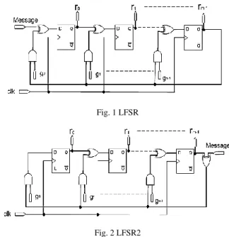
The CRC calculation was realized traditionally in hardware with an LFSR in GF2 configuration as shown in Fig. 1. The polynomial generatordetermines the size and the taps of the shift register [2, 3]. In order to obtain the CRC, the register needs to be cleared in a first step. Then, after injecting the message and 𝑚 additional zeros, by inputting one bit per cycle, the register will hold the desired CRC.A receiver can verify the received message with its appended CRC by simply applying the same procedure, without appended zeros. If there are no errors; the registers finally will hold zeros.
The circuit has been modified according to Fig. 2, which so called LFSR2 in contrast to the first version, which is referred to simply as LFSR,in LFSR2 the message is combined with the most significant register bit to form the feedback,an advantage arises, as no zeros need to be shifted in at the end; that is we multiplying the input polynomial
message with 𝑥𝑚and thus the CRC can be obtained 𝑚 clock cycles earlier [9, 10].
Fig. 1 LFSR
Fig. 2 LFSR2
The generic hardware approach uses an inexpensive linear feedback shift register (LFSR), which assumes serial data input. In the presence of wide data buses, the serial computation has been extended to parallel versions that process whole data words based on derived equations. The fundamental work on parallel CRC computation was introduced by Pei in 1992 [11]. Braun [12] addressed the hardware mapping problem of the parallel CRC algorithm by introducing a slightly different matrix computation technique than Pei.Cheng and Parhi [13]discussed unfolding the serial implementation andcombined it with pipelining and retiming algorithms to increase the speed. [14] Proposed a scheme to calculate CRC in parallel.Walma [15] designed a hardware-based approach, which focus on the pipelining of the CRC calculation to increase the throughput.
Table Lookup Algorithm (TLA) was presented in details in [2]. The main idea of TLA is to calculate CRC by processing the message in units larger than one bit. Candidate quantities are nibbles (4 bits), bytes (8 bits), words(16 bits) and longwords (32 bits) and higher if we can achieve it; ofthese, 4 bits is best avoided because it does not correspond to a byte boundary, at the very least, any speedup should allow us to operate atbyte boundaries, and in fact most of the table driven algorithmsoperate a byte at a time [3]. By comparing TLA with bit wise algorithm in LFSR; we found that TLA has a considerable speed advantage, but TLA need more area than any other algorithm, where every TLA has 256 (28) entries for units of one byte ; each of which is 𝑚 bits, which will increase if the used unit is more than one byte; 65536 (216) entries for two bytes and so on, which won‟t be suitable for applications which need small area for CRC circuits.
50 All Rights Reserved © 2012 IJARCSEE
A number of software-based algorithms have also been proposed [17-21].
IV. PROPOSEDCRCALGORITHM
The proposed CRC algorithm that will be used in the design is Reduced Table Lookup Algorithm (RTLA). Our proposed algorithm is based on the one described by[2] and [8].In our design we used RTLA entries for each bit of input message and calculate CRC of it concurrently.
A. Generating RTLA Table
For calculating CRC in parallel there are two important properties of CRC mathematics must be used; from linearity properties of CRC we can prove the following properties of CRC mathematics:
1. 𝐶𝑅𝐶 𝐴 𝑥 + 𝐵 𝑥 = 𝐶𝑅𝐶 𝐴 𝑥 + 𝐶𝑅𝐶[𝐵 𝑥 ] 2. 𝐶𝑅𝐶 𝑥𝑏 𝐴 𝑥 = 𝐶𝑅𝐶[ 𝑥𝑏 𝐶𝑅𝐶 𝐴 𝑥 ]
From eq. (3) and eq. (4), we can deduce that:
𝐶𝑅𝐶 𝐴 𝑥 = 𝐶𝑅𝐶 𝑎𝑘𝑥𝑘 + 𝐶𝑅𝐶 𝑎𝑘−1𝑥𝑘−1 + ⋯
+ 𝐶𝑅𝐶 𝑎0𝑥0 5
From the last equation, we can drive RTLA, which has𝑘 elements; each of it is the CRC of input bits according to its position in the input message, the CRC of input message will be the result of XOR of CRC of each input binary „1‟ bit.By using the propriety no.2 to deduce the algorithm that will be used for generating RTLA
𝐶𝑅𝐶 𝑎𝑥𝑏 = 𝐶𝑅𝐶 𝑥. 𝑎𝑥𝑏−1 = 𝐶𝑅𝐶[𝑥 𝐶𝑅𝐶 𝑎𝑥𝑏−1 ] (6)
Whereb equalsthe input message degree and the width of that message is (b + 1) bits.
For example if the input width is b+1 = 4 bits we can produce RTLA with 4 elements when the input 𝐴 𝑥 = 𝑥3; in its polynomial form or input 𝐴 𝑥 =1000 in its binary form, we can use eq. (6) to calculate the 4 elements of RTLA:
1) 𝐶𝑅𝐶 𝑎𝑥0
2) 𝐶𝑅𝐶 𝑎𝑥1 = 𝐶𝑅𝐶 𝑥 𝐶𝑅𝐶 𝑎 𝑥0 3) 𝐶𝑅𝐶 𝑎𝑥2 = 𝐶𝑅𝐶 𝑥 𝐶𝑅𝐶 𝑎 𝑥1
= 𝐶𝑅𝐶 𝑥 𝐶𝑅𝐶 𝑥 𝐶𝑅𝐶 𝑎 𝑥0
4) 𝐶𝑅𝐶 𝑎𝑥3 = 𝐶𝑅𝐶 𝑥 𝐶𝑅𝐶 𝑎 𝑥2
= 𝐶𝑅𝐶 𝑥 𝐶𝑅𝐶 𝑥 𝐶𝑅𝐶 𝑥 𝐶𝑅𝐶 𝑎𝑥0
The equation for generating RTLA in general form is:
𝐶𝑅𝐶 𝑎𝑥𝑏 = 𝐶𝑅𝐶[𝑥 𝐶𝑅𝐶[𝑥 … 𝐶𝑅𝐶 𝑎𝑥0 … ]] (7)
So for calculating (b+1) elements of RTLA the following steps will be taken:
1. First we calculate 𝐶𝑅𝐶 𝑎𝑥0 when 𝑎 is binary 1 bit and we store it as 𝐶𝑅𝐶[𝑎0𝑥0].
2. Multiplying previous calculated 𝐶𝑅𝐶by 𝑥; or in other meaning appending binary zero to previous CRC, and eliminate the MSB; then calculate the
current 𝐶𝑅𝐶 and store it as 𝐶𝑅𝐶[𝑎𝑗𝑥𝑗]; where j has a value from 1to b.
3. j in previous step equals 1; so this step will be repeatedb-1timesby increment 𝑗 with one. 4. Store all pervious calculated
b+1elementsinRTLA table.
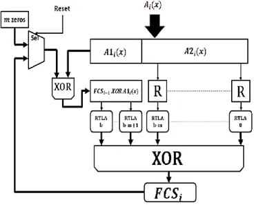
B. Calculating CRC of Two Input Blocks
It will be hard to treat hundreds of bytesof the entire message at once for one cycle, so the proposed design will have one block input with (𝑏+1) bits for one cycle and we will use the same RTLA for all next inputs.
As shown in Fig. 3 if the entire message A(𝑥) consists of two blocks 𝐴1 𝑥 and 𝐴2 𝑥 ; the width of both of them are𝑏 + 1bits ,we will input block 𝐴1 𝑥 then block 𝐴2 𝑥 to calculate CRC[A(𝑥)] .
𝐴 𝑥 = 𝐴1 𝑥 𝑥𝑏+1+ 𝐴2 𝑥 (8)
We will express 𝐴1 𝑥 𝑥𝑏+1 as following:
𝐴1 𝑥 𝑥𝑏+1= 𝐴1 𝑥 𝑥𝑚 𝑥𝑏+1−𝑚 (9)
After adding 𝑚 of binary zeros to 𝐴1 𝑥 ; we can calculate CRC of 𝐴1 𝑥 using (𝑏 + 1) RLTA elements; as shown in Fig. 3:
𝐶𝑅𝐶 𝑥𝑏+1−𝑚 𝐴1 𝑥 𝑥𝑚 = 𝑥𝑏+1−𝑚 𝐶𝑅𝐶 𝐴1 𝑥 (10)
Fig.3 shows that there are two blocks (𝑥𝑏+1−𝑚 𝐶𝑅𝐶 𝐴1 𝑥 and𝐴2 𝑥 ) are equal in degree; for calculating 𝐶𝑅𝐶[𝐴 𝑥 ] we must calculate CRC for both of them:
𝐶𝑅𝐶 𝐴 𝑥 = 𝐶𝑅𝐶 𝑥𝑏−𝑚+1 𝐶𝑅𝐶 𝐴1 𝑥
+ 𝐶𝑅𝐶 𝐴2 𝑥 (11)
By using the propriety no.1; and from the linearity propriety of CRC mathematics we can deduce that:
𝐶𝑅𝐶 𝐴 𝑥 + 𝐶𝑅𝐶 𝐵 𝑥 = 𝐶𝑅𝐶[ 𝐴 𝑥 + 𝐵 𝑥 ]
We will deduce the equation that will be used to calculate the CRC of two input blocks:
𝐶𝑅𝐶 𝐴 𝑥 = 𝐶𝑅𝐶 𝑥𝑏+1−𝑚 𝐶𝑅𝐶 𝐴1 𝑥 + 𝐴2 𝑥 (12)
” +” or addition in CRC mathematics is no carry addition and equal XOR operation of two binary elements as shown in Fig. 3.
51 All Rights Reserved © 2012 IJARCSEE
Fig. 3 CRC calculation of two input blocks with the same RTLA
C. The Proposed Design
Before we start the design, we will divide the 𝑘 input bits of the entire message to 𝑛equal blocks:
𝐴 𝑥 = 𝐴1 𝑥 + 𝐴2 𝑥 + ⋯ + 𝐴𝑛 𝑥 (13)
Where 𝐴1(𝑥) is the first block of the message with the highest polynomial degree;𝑘 degree, and𝐴𝑛(𝑥) is the last
block of the message with the smallest block polynomial degree;bdegree.
Each block 𝐴𝑖(𝑥)is (b+1) bits; where 𝑖 has a value from 1 to 𝑛. By using the propriety no. 1 of previous mentioned properties;we can express 𝐶𝑅𝐶[ 𝐴 𝑥 with the following equation:
𝐶𝑅𝐶 𝐴 𝑥 = 𝐶𝑅𝐶 𝐴1 𝑥 + 𝐶𝑅𝐶 𝐴2 𝑥 + ⋯ + 𝐶𝑅𝐶 𝐴𝑛 𝑥 14
Equation (14) shows that we can calculate CRC[A(𝑥)] by calculating CRC[Ai(𝑥)] of its blocks by using RTLA and
XOR them together.
We will treat each block as an input message with different polynomial degree as its position in entire message and every block has its own RTLA; each RTLA has (𝑏+1) elements and each of them consists of 𝑚 bits;but that will require hardware design of very large area, so in this design we will input just one block 𝐴𝑖(𝑥); from 𝐴1 𝑥 to 𝐴𝑛(𝑥) and
treat each input block as the current input message.
The proposed design shown in Fig. 4, where we assume the input messageis𝐴𝑖(𝑥) with 𝑏 polynomial degree and has (b+1) bits.
The first step of the calculation ;that we will divide Ai(𝑥)
to two blocks A1i(𝑥) and A2i(𝑥),where; A1i(𝑥) has 𝑚 bits as
same as the FCS , and A2i(𝑥) has (𝑏 − 𝑚)bits.
The second step; as we proved in previous section the same hardware with the same RTLA will be used; we XOR between A1i(𝑥) of current input and the FCS of previous
input;𝐹𝐶𝑆𝑖−1.
Fig. 4 Proposed pipelined CRC architecture using RTLA
When we input the first block A1(𝑥); there will be no
previous FCS, so we will use Reset to select between two inputs; the first is 𝐹𝐶𝑆𝑖−1, and the second is 𝑚 of binary zeros which so called the Initial value of the input registers, it will be selected at the first time only; when we input A1(𝑥).
Before using RTLA of input bits we used delay elements𝑅 for𝐴2(𝑥); to synchronize the inputs of all bits into RTLA.
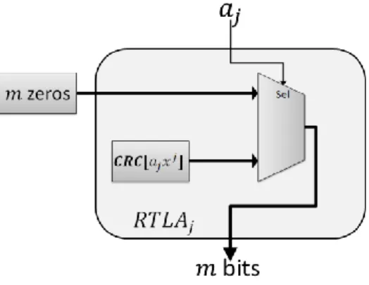
The third step; we use RTLA of 𝑏 elements each of which has 𝑚 bits, every block of RTLA in our design refers to one element of RTLA that referred as 𝑅𝑇𝐿𝐴𝑗; where 𝑗 has a value from 0 to 𝑏 as the position of each input bit to 𝑅𝑇𝐿𝐴𝑗.
As shown in Fig. 5 the input of each RTLA block is one binary bit and was referred as 𝑎𝑗; which select between two input values; the first value is 𝐶𝑅𝐶[𝑎𝑗𝑥𝑗] when 𝑎𝑗 = 1, and the second value 𝑚 bits of binary zeros when 𝑎𝑗 = 0 . As
shown in Fig. 5 the value of 𝑚 bits of binary zeros is the same for all 𝑅𝑇𝐿𝐴𝑗 ,and does not required more area for
every 𝑅𝑇𝐿𝐴𝑗.
The last step of the design is XOR the output of all 𝑅𝑇𝐿𝐴𝑗
and store the result in𝐹𝐶𝑆𝑖, which will hold 𝑚 of bits. This steps will be repeated by inputting𝐴𝑖 𝑥 blocks until we reach to 𝐴𝑛 𝑥 block, and the 𝐹𝐶𝑆𝑛 will be the result of 𝐶𝑅𝐶[𝐴 𝑥 ].
52 All Rights Reserved © 2012 IJARCSEE
Fig. 5 RTLA architecture of one element
V. CRC32IMPLEMENTATION
To implant the proposed design on FPGA we used the XILINX Virtex-6 device and the Xilinx ISE Design Suite. We usedModelSim simulator to verify the design
We used the following CRC32 polynomial:
𝐶𝑅𝐶32 = 𝑥32+ 𝑥26+ 𝑥23+ 𝑥22+ 𝑥16+ 𝑥12+ 𝑥11+ +𝑥10 +𝑥8+ 𝑥7+ 𝑥5+ 𝑥4+ 𝑥2+ 𝑥 + 1
Where, 32 inCRC32 refers to the degree of the polynomial generator. The synthesized results of the implementation of CRC32 are shown in Table I.In this table there areseven different results according to the data input width ; the RTLA size in bytes, the area according to LUT of FPGA, maximum frequency, and data throughput at one clock cycle. From Table I we cansee that the area and throughput are proportional to the data input width, and the maximum frequency nearly the same; which make doubling the data input width approximately doubles the data throughput of that input, therefore we can control in the data throughput by controlling in the width of the input data.
As shown in Table I we can choose any width for data input during the design which aren‟t units of generator polynomial width such as input of 100 bits, 200 bits and 240 bits.
The results of proposed design in Table I shows that it has high maximum frequency and high data throughput with more than 100 Gpbs when the data input width is 200 bits; and that data throughput increases by increasing the data input width.
To compare our CRC32 implementation with others we mapped our design to the Altera Stratix II device. The synthesis result for the proposed design is shown in Table II. The synthesis results of CRC32 for [14] and [15] is shown in Table III and Table IV respectively.
TABLEI
SYNTHESISRESULTSFORPROPOSEDDESIGNOFPIPELINED CRC32
Data Input ( Bits)
RTLA (Bytes)
Area (LUT)
Max. Frequency ( MHz)
Data Throughput
(Gbps)
32 128 143 571.233 18.297
64 256 255 567.118 36.295
100 400 389 563.349 56.334
128 512 485 545.548 69.830
200 800 725 547.046 109.409
240 960 856 544.751 130.740
256 1024 909 566.476 145.017
TABLEII
SYNTHESISRESULTSFORPROPOSEDDESIGNON ALTERASTRATIXIIDEVICE
Data Input ( Bits)
Area (LUT)
Max. Frequency
( MHz)
Data Throughput
(Gbps)
32 139 361.011 11.5
64 242 318.9 20
100 340 297 29.7
128 404 288.4 36.8
200 584 280.5 56.1
240 700 275.8 66.1
256 705 277 70.9
From Tables (I, II) we notice that the maximum frequency of the same proposed design in Table IIis less than that in Table I that is due to the difference of the two FPGA devices which are used.Fig. 6 shows the maximumfrequency for Virtex -6 and Stratix II devices, the results shows that the maximum frequency of the two devices is almost fixeddue to the parallel implementation of pipelined architecture of the proposed design; but you can notice that the maximum frequencyof Virtex-6 is more stable than that of Stratix II and has maximum frequencies.
Fig. 7shows the synthesis results of the maximum frequency in MHz for datainputs (64,128 and 256 bits). Fig 8shows the synthesis results of the area in LUT of the FPGA for data inputs (64,128 and 256 bits).
Fig. 6 The Maximum frequency of Virtex-6 and Stratix II for the proposed design
0 100 200 300 400 500 600
32 64 100128200240256
Max.
Freq
u
e
n
cy
(MH
z)
Data Input (Bits)
Virtex-6
53 All Rights Reserved © 2012 IJARCSEE
TABLEIII
SYNTHESISRESULTSFOR[14] Data Input ( Bits) Area (LUT) Max. Frequency ( MHz) Data Throughput (Gbps)
64 398 185 11
128 1050 124 15.8
256 3075 86 22.0
TABLEIV
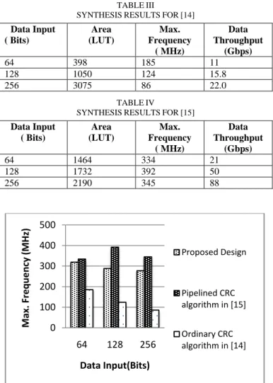
SYNTHESISRESULTSFOR[15] Data Input ( Bits) Area (LUT) Max. Frequency ( MHz) Data Throughput (Gbps)
64 1464 334 21
128 1732 392 50
256 2190 345 88
Fig.7: Synthesis results of the max. frequency
From Fig. 7 it is clear that the frequency of the proposed design is nearly fixed, although the design of [15] has data throughput faster than that of the proposed design; but its area with 64 bit input is nearly twice the area with 256 bit input of the proposed design. Fig. 8shows that the large difference in the amount of area among the three designs, the area of the proposed design is much smaller than other designs and appropriate nearly linearly with the width of data inputs.
Fig.8:Synthesis results of the Area
From previous results it is clear that the proposed design has relatively high data throughput and very low area with respect to the other designs.
VI.CONCLUSION
We presented in this paper a fast CRC algorithm with a new design of low area pipelined architecture using RTLA, which depends only on the positions of binary „1‟in input bits and the generator polynomial. Generating RTLA elements using fast algorithm was presented to calculate RTLA elementswith the same number of input message bits for the certain CRC polynomial.The proposed design can be used for inputting any length of data with slightly increase of area and almost the same frequency due to parallel processing of input data and pipelined architecture of the design. We proved that the proposed design has very low area and high data throughput by implementing CRC32 on FPGA using VHDL with different data input widths, we used XILINX Virtex-6 FPGA to obtain data throughput more than 100 Gbps using data input width of 200 bits; and by increasing the data input width we got 145 Gbps of data throughput. We compared the syntheses results of our design with others using Stratix II FPGA and the same syntheses tools and we proved that; the proposed design has speed up the CRC calculation while maintaining very low area, and by comparing the results of Virtex-6 and Stratix II FPGA; we found that Virtex-6 is more stable in its max. frequency and much more that of Stratix II.The proposed design is suitablecandidate for communication protocols which required high datathroughput requirement more than 100 Gbps such as Ethernet protocolIEEE 803.2ba 100 Gbps.
REFERENCES
[1] W. W. Peterson and D. T. Brown, "Cyclic Codes for Error Detection," Proceedings of the IRE, vol. 49, no. 1, pp. 228 - 235, 1961.
[2] T.Ramabadran and S. Gaitonde, "A tutorial on CRC computations," Micro IEEE, vol. 8, no. 4, pp. 62-75, Aug. 1988.
[3] Ross N. Williams. (1993, Aug.) Painless Guide to CRC Error Detection Algorithms. [Online]. www.ross.net/crc/crcpaper.html [4] S. Lin and D. J. Costello, Error Control Coding, 2nd ed. Upper Saddle
River, New Jersey, USA: Pearson Prentice Hall, 2004.
[5] A. Tanenbaum, Computer Networks, 4th ed. Upper Saddle River, New
Jersey, USA: Prentice Hall, 2003.
[6] P. Koopman, "32-Bit Cyclic Redundancy Codes for Internet Applications," in DSN 2002 : Proceedings of International Conference on Dependable Systems and Networks., Washington, DC, USA, 2002, pp. 459 - 468.
[7] P. Koopman and T. Chakravarty, "Cyclic Redundancy Code (CRC) Polynomial Selection For EmbeddedNetworks," in DSN 2004: Proceedings of International Conference on Dependable Systems and Networks., Florence, Italy , 2004, pp. 145 - 154.
[8] J. Ray and P. Koopman, "Efficient high hamming distance CRCs for embedded networks," in DSN 2006 : Proceedings of International Conference on Dependable Systems and Networks., Philadelphia, PA ,USA, 2006, pp. 3 - 12.
[9] G. Campobello, G. Patane, and M. Russo, "Parallel CRC relization," IEEE Transactions on Computer, vol. 52, no. 10, pp. 1312-1319, Oct. 2003.
[10] M. Grymel and S.B. Furber, "A novel programmable parallel CRC ciruit," IEEE Transactions on Very Large Scale Integration (VLSI) Systems, vol. 19, no. 10, pp. 1898-1902, Oct. 2011.
[11] T.-B. Pei and C. Zukowski, "High-speed parallel CRC circuits in VLSI," IEEE Transactions on Communications, vol. 40, no. 4, pp. 653 - 657, Apr. 1992.
0 100 200 300 400 500
64 128 256
Max. Frequ enc y (MHz ) Data Input(Bits) Proposed Design Pipelined CRC algorithm in [15]
Ordinary CRC algorithm in [14]
0 500 1000 1500 2000 2500 3000 3500
64 128 256
Area
(LUT
)
Data Input (Bits)
Proposed Design
Pipelined CRC algorithm in [15]
54 All Rights Reserved © 2012 IJARCSEE
[12] M. Braun, J. Freidich, T. Grun, and J. Lembert, "Parallel CRC computation in FPGAs," Proc. Workshop Field Program. Logic Appl., pp. 156-165, 1996.
[13] Chao Cheng and K.K. Parhi, "High-speed parallel CRC implementation based on unfolding, pipelining, and retiming," IEEE Transactions on Circuits and Systems II: Express Briefs, vol. 53, no. 10, pp. 1017 - 1021, Oct. 2006.
[14] A. Simionescu. (2001) CRC tool computing in parallel for ethernet. [Online]. http://www.nobugconsulting.com/crc_details.pdf
[15] M. Walma, "Pipelined Cyclic Redundancy Check (CRC) calculation," in ICCCN 2007,Proceedings of 16th International Conference on Computer Communications and Networks, Honolulu, HI, USA, 2007, pp. 365 - 370.
[16] Yan Sun and Min Sue Kim, "A table based algorithm for pipelined CRC calculation," in Communications (ICC), 2010 IEEE International Conference, Cape Town, South Africa, 2010, pp. 1 - 5. [17] S.M. Joshi, P.K. Dubey, and M.A. Kaplan, "A new parallel algorithm
for CRC generation," in ICC 2000, IEEE International Conference on Communications, New Orleans, LA ,USA, 2000, pp. 1764 - 1768. [18] M.E. Kounavis and F.L. Berry, "Novel table lookup-based algorithms
for high-performance CRC generation," IEEE Transactions on Computers, vol. 57, no. 11, pp. 1550 - 1560, Nov. 2008.
[19] D. Sarwate, "Computation of cyclic redundancy checks via table lookup," Communications ACM, vol. 31, no. 8, pp. 1008-1013, Aug. 1988.
[20] D. Feldmeier, " Fast software implementation of error dtection codes," IEEE/ACM Transactions on Networking, vol. 3, no. 6, pp. 640 - 651, Dec. 1995.