JEEECCS, Volume 2, Issue 3, pages 1-12, 2016
Reconfigurable computing in hardware security
A brief review and application
Fernando Georgel Bîrleanu
Faculty of Electronics, Communications and Computers
University of Pitesti Pitesti, Romania [email protected]
Nicu Bizon
Faculty of Electronics, Communications and Computers
University of Pitesti Pitesti, Romania
Abstract – The first part of this paper is a brief review of
reconfigurable computing in hardware security and focuses on devices designed with Field-Programmable Gate Arrays technology. The study is focused on reconfigurable computing with FPGAs versus ASICs, hardware security of FPGAs, and how all these are applied to hardware security devices under usual attacks. The second part presents the design of an application proposed to secure sensitive data and information. In comparison with other proposals, the main advantages and features of this application are: highly protected data on the SD card compared with software solutions because the device is designed only with hardware elements, transferring data speed is limited only by SD card specifications, and unique encrypt/decrypt PIN code restricts other users access to non-belonging files. The experimental results confirm the design considering the features mentioned.
Keywords: reconfigurability, data security, FPGA, attack LCD, SD card, UART, encryption/decryption, device control, FSM.
I. INTRODUCTION
Personal information security and data security is a major problem for humanity since many years ago. All started with antique mechanisms and evolved to more and more ingenious electronic solutions.
We live in a global connected world with easy to steal information where identity theft is a threat that people are not really aware of [1]. Therefore, new reliable security methods were necessary to keep up. An efficient solution to secure all these sensitive data is reconfigurable computing.
Reconfigurable computing, the use of programmable logic to accelerate computation, arose in the late 80’s with the widespread commercial availability of Field-Programmable Gate Arrays (FPGAs) [2].
In traditional computing there are two ways to execute different algorithms in order to achieve security: to use an Application Specific Integrated Circuit (ASIC), or to use microprocessors. The first solution is very fast and efficient but ASICs are designed to perform a given computation, and the chip cannot be modified after the fabrication process [3] [4]. The second solution is more flexible because the software instructions can be changed in order to
modify the system functionality without changing the hardware. But there is a major inconvenient: performance. To complete these disadvantages between hardware and software we use reconfigurable computing [4].
Field-Programmable Gate Arrays are digital integrated circuits (ICs) designed to be configured (programmed) to perform a vast variety of tasks [5]. FPGAs contain configurable logic blocks (CLBs) with configurable interconnects between these CLBs [6]. The FPGA term has a more historical connotation because these circuits are not only reconfigurable circuits, able to implement complex logic functions, as they were at the beginning. Today, in an FPGA chip we find RAM (Random Access Memory) memory blocks, hardware multipliers, and even DSP (Digital Signal Processing) cells based on combined MAC (Multiply Accumulate) operation.
These advanced computational elements allow to transform FPGA in an extraordinary computation machine, and today, this industry is the most profitable among all electronic industries.
According to [7], and [8], the main advantages of FPGA design are: faster time-to-market, simpler design cycle, field programmability, more predictable project cycle, and no upfront non-recurring expenses (NRE). When using ASIC design, the advantages are: full custom capability, smaller form factor, and lower unit costs. For a better understanding, let’s take a look at FPGA vs. ASIC design flow comparison [7] [8].
If we take a look at the process technology in fabricating FPGAs, and ASICs, we should see that over years FGPAs circuits are in significantly growing advantage versus ASICs circuits, as we can observe in the chart of Figure 2 [9].
Figure 2. Process technology - ASIC vs. FPGA – caption adapted from [9].
In order to configure the FPGA circuit, (in general) we use hardware description languages (HDL), such as VHDL (VHSIC HDL - Very High Speed Integrated Circuit Hardware Description Language), used to describe digital electronic systems [10] [11].
Thus, the structure of this study is the following.: the first section is an introduction to reconfigurable computing, insisting on FPGAs versus ASICs, the second one refers to hardware security of FPGAs, the third section presents usual attacks, and how these are applied to hardware secured devices, the next two sections present an application proposed to secure sensitive data and information, including the results obtained, and the last section concludes the paper.
II. HARDWARE SECURITY OFFPGAS
To hardware secure a device designed using FPGA technology, we must take care of two aspects: device security, and data security. Device security means that the designer must protect the FPGA design, or device. Data security refers to the function configured into the circuit that must meet some critical security goals like data authenticity, or data integrity. If the device security doesn’t exist, it is very hard to implement performant data security. Therefore, these two aspects must coexist. [12] [13].
FPGA device security is necessary to prevent some common actions that bad intended people can try to execute, depending on what they want to obtain, like:
Cloning – when someone manages to reproduce your design for sale. He can buy the components of the design, and he doesn’t care about the identical operations of your device, because these can be duplicated. As an example, for the SRAM based FPGA, this can be done by intercepting the configuration bitstream from the boot PROM [1] [14].
Overbuilding – when someone like a manufacturer makes more copies of your
device than you have ordered. These copies can be sold, and the profits will end at the manufacturer [1] [14].
Reverse engineering – when someone manages to find out how your device operates, behave, and then uses, or even makes it better [1] [14].
Figure 3, and Figure 4 shows the classic hardware security architecture for SRAM based FPGA, and Flash based FPGA.
Figure 3. SRAM FPGA security architecture – caption adapted from [12].
Figure 4. Flash FPGA security architecture – caption adapted from [12].
In general, FPGA data security refers to security applications that can be designed, and implemented using FPGA technology, as those below:
Data encryption/decryption – a method of encoding information in a way that only authorized people/devices can read it. Over the last decades, a large variety of standards have been developed in order to ensure high information security. Some of these standards are: Triple-DES, AES (Advanced Encryption Standard), DES (Data Encryption Standard), RSA, OpenPGP, CipherSaber, IPsec, CAST,
SRAM FPGA Configuration
Flash PROM (external)
AES decryption CRC
AES KEY AES key Security
lock-bit(s)
OTP (anti-fuse) SRAM Flash Logic
Flash
Logic
Flash FPGA Configuration (Flash ROM, eNVM)
128-bit AES key Security lock-bits
128-bit FlashLock Passcode
Match? Flash Security Segment
Strong message authentication
128-bit AES decryption
JTAG input
Y/N
Programming disabled
Plaintext bitstream
Decrypted bitstream
RC4, and RC6. With this large variety of tandards, and the customized implementation possibilities for each standard, cryptography can be seen as one of the most versatile application domains of computer science. [15]
Authentication of hardware/software/people – authentication technologies are usually based on one of three things: something the individual knows, such as a password; something the individual has, such as a physical key, or secure token; and something the individual is, or does [16].
Enciphered data storage – refers to a cryptographic transformation that should prevent reversal transformation on a hard, or flash disk. One of the oldest ciphers used long time ago is Caesar’s cipher, consisting of a cipher text alphabet produced by a three positions to the left rotation of the source alphabet [17].
Key management – is the control and management of all the cryptographic resources, and involves the devices that are used to generate, to distribute, and to load keys [18].
Anti-reverse engineering – mechanisms implemented in the device used to cover some essential parts of the design in order to avoid this behavior.
Anti-tamper – tamper mechanisms are designed to prevent physical, or electronic action against the device, and they are divided into four groups: resistance, evidence, detection, and response [18] [19].
In order to be secured, a device must stay in a secure location with secured communications interfaces, and, if the location is unprotected to physical attacks, then the device will have to be tamper-resistant.
III. SECURITY ATTACKS
Simply for fun, or with bad intension, there are people, also known as hackers, who provide different purpose attacks, depending on what they want to achieve [14]. The level of importance to protect against these attacks is given by a simple fact: how sensitive the data stored in the attacked device is. In Figure 5, we can see the inverse relationship between the knowledge that attackers have, and growing sophistication of these attacks, from the beginning of 1980 to 2010 [20].
In the last years, the level of sophistication, and complexity of the attacks increased more and more, making more difficult to implement the defense against them, using the current algorithms. So, new defense algorithms must be proposed against hackers’ attacks.
Figure 5. Growing attack sophistication versus decreasing intruder knowledge – caption adapted from [20].
According to IBM [21], hackers can be grouped in three categories:
Clever outsiders – they have access to poor and moderately attacking equipment, and they use system vulnerabilities rather than designing them [1].
Knowledgeable insiders – they have high technical experience, and highly sophisticated equipment to create attacks.
Funded organizations – groups of specialists capable of extreme advanced attacks with the latest analysis tools [1].
Main types of technical attacks, depending on the analyzed parts of the device, are [22] [23] [24]:
Software attacks – man-in-middle, DoS (Denial of Service), eavesdropping, cryptographic attacks [25].
Side-channel attacks (passive) – timing analysis, SPA (Simple Power Analysis), DPA (Differential Power Analysis), and EME (Electromagnetic Emanations) [25].
Active attacks – clock manipulation, temperature attacks, fault injection [26].
Semi-invasive and invasive attacks – optical attacks, electron microscope, and focused ion beam [26].
An attack example on a device based SRAM FPGA is cloning it when is programmed at a power-up. The method involves simply connecting to the JTAG interfaces wires, and observes all the signals using logic analyzers. Then, these signals are analyzed, and the attacker can relay the commands in his personal device. He can also modify the bitstream in order to hide cloning [28].
Another attack example, known as data remanence, is against SRAM memories, where security reconfigurable circuits store secret information like encryption keys. SRAM power disappears when the device is tampered, and below -20C temperatures memory content can be ”frozen”. Usually, at these temperatures most circuits signalize tamper events. So, some useful information can be extracted from erased memories. In order to avoid this to happen, temperature detection circuits can be used, or prevent storing cryptographic data for a long time in SRAM [14].
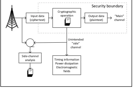
Figure 6 reveals how side-channel attacks works.
Figure 6. Side-channel attacks – caption adapted from [12].
There are devices that are including cryptography methods when designed. For those methods, U.S. government agencies must use FIPS (Federal Information Processing Standards) PUB 140-3 validated cryptographic products with five possible security levels to receive validation [22]:
Security level 1 – specifies basic security requirements for a cryptographic module as specifications, approved algorithms, and approved modes of operation [29].
Security level 2 – improves level 1 by adding tamper evidence, and role-based or identity-based authentication [29].
Security level 3 – adds the following requirements: the input, or the output of CSP (critical security parameters), is separated using trusted channel from other ports and interfaces, the authentication is identity-based, tamper response and zeroization circuitry, protection against timing analysis attacks, and integrity tests [29].
Security level 4 – improves level 3 with two-factor authentication, encryption, and decryption of CSP, integrity test code, protection against SPA (Simple Power Analysis) and DPA (Differential Power Analysis) attacks, and extended auditing requirements [29].
Security level 5 – provides the highest level of security by adding protection of PSP (Public Security Parameters) from EME (Electromagnetic Emanations) attacks, encryption and decryption of PSP, opaque to non-visual radiation examination, zeroization of PSP’s and protection from tamper detection, and zeroization circuitry disablement [29].
IV. DESIGN OF APPLICATION
In this section, the Hardware and Software design of device, used to store safe data on SD (Secure Digital) card, is shown. This device is designed using FPGA technology with ML507 development board built with FPGA Virtex 5 family. In order to provide a correct device functionality, the firmware I have implemented respects the following:
Device access and data access is made through a PIN (Personal Identification Number) code.
The SD card is used to store encrypted data, and also to read existing data.
An alphanumeric 2x16 LCD (Liquid Crystal Display) shows different messages when the device is in function.
Device – computer communication is UART (Universal Asynchronous Receiver/ Transmitter).
AES-128 (Advanced Encryption Standard) is the cryptographic algorithm for data encryption/decryption.
The authentication PIN code is stored in a SRAM (Static Random Access Memory).
Data transfer is initiated through a software application, after correct PIN code authentication. Correct or incorrect PIN code is signalized on the LCD. After authentication, desired operation can be selected between storing and reading. If this is a store operation, then you must select the files that should be transferred. If this is a read operation, then you must select where to transfer the files.
AES-128 is a standardized algorithm for block symmetric encryption, used today in many applications and secure devices. The key length for encryption/decryption is 128 bits, and it is generated based on an encrypt/decrypt PIN code. This code length is up to 16 characters, and there is a very important aspect: it is not stored. The user chooses it and introduces it into the software application.
While the device is running, the display shows various messages in order to signalize its status: Input data
(ciphertext)
Cryptographic
operation Output data (plaintext)
Security boundary
Main channel
Side-channel
analysis Timing information Power dissipation Electromagnetic
fields Unintended
”INCORRECT PIN”.
”DEVICE CONNECTED”.
”STORE FILES”.
”READ FILES”.
”ENCRYPTING FILES”.
The entire assembly is controlled with a general module. This module provides synchronicity for components, correct device functionality, and signaling.
Figure 7 shows the device block diagram, and a theoretical view of how the device should look.
Figure 7. Device block diagram.
In the following, I will show how the main modules where designed and implemented in VHDL, using Xilinx ISE Design Suite.
A. FPGA - LCD communication
The LCD is used to show different messages, when the device is running. It was necessary to implement the communication LCD controller instruction set (Table 1).
The display works in 4-bit mode, but to send instructions or to WR/RD (write/read) information, the DB7, DB6, DB5, and DB4 pins are used. These four pins form a data bus. RS (Register Select) pin controls write/read information, or instructions mode:
”0” – LCD instructions mode.
”1” – WR/RD data mode. [40]
RW pin controls read/write operation:
”0” – write operation.
”1” – read operation. [40]
Table 1. LCD instruction set - caption [40].
E (Enable) pin points the start of WR/RD operation, when enabled (”1”) [40].
Before showing information, the display must be initialized using instruction set in Table 1. In Figure 8, the initialization flow chart is shown [40].
Figure 8. LCD initialization flow chart - caption [40].
After initialization ends, write/read operation can start. For this to happen, timing diagrams and corresponding times must be observed, as shown in Figure 9, Figure 10, Table 2, and Table 3 [40]. FPGA
VIRTEX-5
USB (UART)
SD CARD
POWER SUPPLY
16x2 CHARACTER LCD PC
Figure 9. Timing diagram for write operation – caption [40].
Figure 10. Timing diagram for read operation – caption [40].
Table 2. Write operation (timing values) – caption [40].
Table 3. Read operation (time values)– caption [40].
According to previous information, in Figure 11 I designed the block diagram of FPGA - LCD communication, which was also implemented in VHDL [30] [31] [32] [33].
Figure 11. FPGA – LCD communication block diagram.
The Data_in signal, from SEND_TO_LCD block, is 256 bits in length, because the display has 32 characters (32 characters * 8 bits/character = 256 bits).
Messages displayed on LCD are stored inside the FPGA circuit in a block RAM, and, within the block diagram, as shown in Figure 11, all 32 characters can be display at a time.
In the SEND TO LCD block, the LCD is initialized, and input data is transferred nibble by nibble to the LCD CONTROLLER block, respecting timing diagrams.
The block RAM is 32x256 organized, and Figure 12 shows its block diagram [30] [31].
Figure 12. RAM 32x256 block diagram.
Figure 13 reveals the memory map. Unused areas can be used in future device improvements.
Figure 13. RAM 32x256 map.
B. FPGA - SD card communication
The SD card is used to store encrypted data. Because ML507 development board does not support SD card connector, I connected one at the XGI expansion pins, as shown in Figure 14 [39].
SEND TO LCD LCD CONTROLLER clock
reset
LCD_RS LCD_RW LCD_E LCD_DATA
}
TO LCD
4 data_out data_in
rs rs rw rw
4
start start busy busy
4
256 data_in
RAM32x256 clock
wr_data wr_addr wr_en
rd_data
rd_addr 256
5
5
256
UNUSED AREA
OPERATION ERROR
OPERATION SUCCEEDED ENTER DECRYPT PIN
ENTER ENCRYPT P IN DECRYPTIN G FILES
ENCRYPTING FILES TRANSFER FILES PC - SD CARD
TRANSFER FILES SD CARD - PC INCORRECT PIN CODE
CORRECT PIN CODE ENTER PIN CODE
DEVICE CONNECTED
INFORMATIVE MESSAGES AREA
08h 09h 00h
Figure 14. SD card connection to ML507 – caption [39].
The SD card communication is realized in two modes: SD mode, and SPI (Serial Peripheral Interface) mode. The default mode is SD, but for this application I used SPI mode which runs using a master/slave set-up, and it can work in full duplex mode. Figure 15 illustrates SPI communication method [37].
Figure 15. SPI communication method – caption [37].
Communication with SD card is realized by sending and receiving commands. Commands are 48 bits in length (Figure 16), and responses are 8 bits in length, with two exceptions of where 40 bits responses are received (Figure 17 and Figure 18) [37].
Figure 16. 48 bits command – caption [37].
Figure 17. 8 bits response – caption [37].
Figure 18. 40 bits response) – caption [37].
In Table 4 we can see the commands set for SPI mode.
Table 4. SPI commands set – caption [37].
Before using it to store data, the SD card needs to be initialized, as shown in Figure 19, and then, data transfer can start, as shown in Figure 20 [37]. The card also supports single and multiple block reading, and also single and multiple block writing.
SD CARD CONTROLLER clock
reset
data_in data_mode_in
data_out
wr
8 8
rd miso
cs mosi sclk
Figure 20. Data transfer – caption [37].
According to previous information, Figure 21 shows the block diagram design of the FPGA – SD card communication, also implemented in VHDL [30] [31] [32] [33].
Figure 21. FPGA – SD card communication block diagram.
C. FPGA - UART communication
I/O serial transfer is done through a single wire for each direction. UART communication is asynchronous because clock signal is not transmitted. The receiver recognizes individual binary values without common clock line. UART interface involves two parts [30] [31]:
Receiver (RX) – converts serial bit flow to parallel data.
Transmitter (TX) – converts parallel data to serial bit flow.
An important problem, in serial transmission, is data reconstruction as it gets to the receiver. Both the transmitter and the receiver must work at the same frequency, and logic is necessary to exist on phase detection (for transmitted data), and for synchronizing the receiver clock. Therefore, one start bit and one or two stop bits are used when the transmission begins. The receiver synchronizes the clock after the start bit, and then starts sampling data bits. If stop bits are not received, the receiver thinks its clock is dephased, and frame error is declared [32] [33].
Figure 22 shows the functional UART diagram, and in Figure 23 UART frame is explained.
Figure 22. UART functional diagram – caption [42].
Figure 23. UART frame format – caption [41].
According to previous information and theory, in Figure 24 I designed the block diagram for FPGA – UART communication which was also implemented in VHDL. In UART CONTROLLER block the following are implemented: RX clock generator, TX clock generator, RX FSM (Finite State Machine), TX FSM and data memory registers. TX/RX UART block is used to declare data for transmission/reception. The messages that appear on UART application are written inside FPGA chip in a RAM block with a 1kx8 organization.
Figure 24. FPGA – UART communication block diagram.
D. AES-128
AES-128 represents a standardized algorithm for block symmetric encryption that can process data blocks of 128 bits length using key cipher of 128, 192 or 256 bits length. In this application, for the key cipher I used a 128 bits length. The encryption process transforms the information into an unintelligible form, called cipher text. Cipher text decryption transforms this new information into original information, called plain text. Figure 25 shows the steps of the encryption process, and Figure 26 shows the operations of the decryption process [34] [35] [36].
TX/RX UART UART CONTROLLER
clock reset
RX
TX
}
TO UART tx_data
tx_data_enable tx_chn_ready rx_data rx_data_enable
8
Figure 25. AES-128 encryption process – caption [35].
Figure 26. AES-128 decryption process – caption [35].
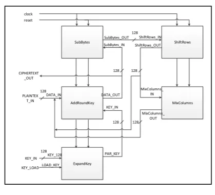
As it can be observed in Figure 25 and Figure 26, each process consists of different transformations applied to data blocks, in a fix number of iterations, called rounds. This number depends on key length. In this case, we have a number of 10 rounds. For each, a round key is generated by the key expansion process. Each step of the encryption process is presented in Figure 27, Figure 28, Figure 29, and Figure 30. In Figure 31, the key expansion process is illustrated. For decryption is the same thing, but backwards [34] [35] [36] [38].
Figure 27. Sub Bytes step – caption [35].
Figure 28. Shift Rows step – caption [35].
Figure 29. Mix Columns step – caption [35].
Figure 30. Add Round Key step – hardware implementation – caption [35].
Figure 31. Key expansion process – caption [35].
The next image, in Figure 32, shows a block diagram of how the AES-128 encryption algorithm should be implemented.
Figure 32. AES-128 encryption process – caption [35].
Figure 33. AES-128 implemented block diagram (data encryption).
E. FPGA – SRAM communication
After the device is connected, on the UART application the authentication PIN code is requested, and it is compared with the one stored in the SRAM. If they are the same, write/read operation can start. Otherwise, the PIN code is again requested, and, after 3 fails, the device blocks for 30 seconds.
The SRAM controller block diagram is illustrated in Figure 34 [30] [32].
Figure 34. SRAM controller block diagram.
F. Device control – main FSM (Finite State Machine)
The main flow chart for implementing this hardware device is shown in Figure 35. Based on this flow chart, the full ensemble works as it was designed. The state where the device is at particular time is signalized on the display synchronized with the performing operations, noticeable on UART application. When the device starts, the device name is displayed. In UART application, the device name appears, and, after 2 seconds, a message says to press ”ENTER” key from the keyboard, in order to continue. After the key is pressed, the PIN code is necessary, and it is up to 16 characters in length. When the code is inserted instead of each character, the symbol “*” appears because of safety reasons. If the PIN code is shorter than 16 characters, the rest is automatically completed with “*”. After “ENTER” is pressed, the code is compared with the one in the SRAM. If they are not the same, the PIN can be inserted again. After 3 fails, the device blocks for 30 seconds to prevent brute force or other attacks to break the algorithm, and, then it comes back to initial settings. If the two codes correspond, write/read
operation can start on/from SD card. For write operation, a cipher PIN code is requested. This code is unique depending on the user and it is used in the encryption process. Then, the files are selected, and, while they are transferred on SD card, they are also encrypted. For reading operation, the decryption PIN code is requested and it must be the same with the cipher PIN code when the files were written. After 3 fails, the device blocks for 60 seconds to prevent brute force. If the introduced code is the same, then the decryption process starts.
Figure 35. Main flow chart.
For the messages displayed on the UART application, an FSM (Figure 36) [30] [31] is implemented, consisting of individual message modules. These modules are controlled with two signals: “start” and “ready”. Also, in this FSM there are signals that control others components (LCD, SRAM, AES-128, SD card) in the same way through smaller modules, in order to perform a correct and synchronous functionality.
Figure 36. Device FSM.
SubBytes ShiftRows clock reset SubBytes_OUT 128 128 MixColumns AddRoundKey ExpandKey SubBytes_IN ShiftRows_IN DATA_OUT DATA_IN PLAINTEX T_IN KEY_IN PAR_KEY KEY_IN KEY_128 LOAD_KEY KEY_LOAD ShiftRows_OUT MixColumns_ IN 128 MixColumns_ OUT CIPHERTEXT _OUT 128 128 128 128
INIT 200 ms POWER- UP
RD / RW? ENTER PIN CODE ENTER DECRYPT PIN CODE RD RW CORRECT PIN CODE? CORRECT PIN CODE? DATA PC - FPGA YES START ENCRYPTION STOP ENCRYPTION DATA FPGA – SD
CARD
STOP DATA
SD CARD - FPGA START DECRYPTION STOP DECRYPTION DATA FPGA - PC
STOP NO ENTER ENCRYPT PIN CODE YES INC CONTOR1 COUNTER1 = 3? WAIT 30 SEC YES NO INC COUNTER2 COUNTER2 = 3? WAIT 60 SEC YES NO NO FSM DEVICE CONTROL CONTROL SHOW THESIS NAME clock reset SHOW PRESS ”ENTER” SHOW ENTER PIN CODE CHECK PIN CODE SHOW CORRECT/ INCORRECT PIN CODE CHOOSE WRITE/READ SD CARD CHECK WRITE/READ OPTION SHOW ENCRYPTING/ DECRYPTING FILES SHOW OPERATION SUCCEEDED SHOW OPERATION ERROR SHOW WAIT 60/120 SECONDS CHECK DECRYPT PIN CODE SHOW ENTER DECRYPT PIN CODE SHOW ENTER ENCRYPT PIN CODE
V. RESULTS
In this section, the results after the device is designed using captures with the software application, and a photo with the device in use are shown. The software application is used through PuTTY terminal. As it can be seen, the device is designed according to Figure 35, and Figure 36. To start transferring data, the PIN code is required. A message is visible on the UART terminal, and on the display, depending on the inserted PIN code. When this is correct, the user must select the operation mode, and, then, the encrypt/decrypt code is required depending on the chosen operation. After the operation end, and the data are encrypted or decrypted, the user can select to start again other operation or to exit.
VI. STATEOFTHEART
According to [43], in present there are 865 hardware and software products incorporating encryption from 55 different countries. Two-thirds of the total are outside the US, with 56% available for sale and 44% free. The main types of these encryption products are: file encryption, message encryption, mail encryption, disk encryption, cloud encryption, telephone, network, browser, VPN, USB, and VoIP.
Safexs Guardian XT and Safexs Protector XT, designed by Safexs from Sweden, are commercial secure flash drives used to secure sensitive data from unauthorized access. The main features of these products are: brute force protection, tamperproof, anti-tampering, password policy, updatable, computer protection, auto-destruct, strong metal alloy, and fast data transfer. However, the data transfer is limited by USB protocol.
Both products use AES-256 hardware encryption algorithm, but unique encrypt/decrypt PIN code used in encryption/decryption process, as in this study, is missing.
VII. CONCLUSION
The usefulness of reconfigurability can be seen on the previously presented device. Because the device is designed only with hardware elements, the data stored on the SD card is highly protected compared with a software solution. Transferring data speed is limited only by SD card specifications.
The session key for encryption/decryption algorithm is temporarily generated, and by using different PIN codes, two or more users can store encrypted files. The unique encrypt/decrypt PIN code restricts other users access to non-belonging files. This PIN code can be extended to alphanumeric code. As a result the security level is enhanced.
The device that was designed to safely store data on SD card is a prototype that can be built as a mobile one.
Thus, the rigidity of hardware systems eliminates the possibility of external actions increasing the security level compared with software implementations.
REFERENCES
[1]B. Badrignans, J. L. Danger, V. Fischer, G. Gogniat and L.
Torres, “Security Trends for FPGAs – From Secured to Secure Reconfigurable Systems, Springer, Dordrecht, 2011, pp. 1 – 21.
[2]M. Gokhale and P. S. Graham, “Reconfigurable Computing –
Accelerating Computation with Field-Programmable Gate Arrays”, Springer, Dordrecht, 2005, pp. 1.
[3]K. Compton, S. Hauck, “Configurable Computing: A Survey
of Systems and Software”, Northwestern University, Dept. of ECE Technical Report, 1999.
[4]K. Compton, S. Hauck, “An Introduction to Reconfigurable
Computing”, Motorola.
[5]C. Maxfiled, “The Design Warrior’s Guide to FPGAs –
Devices, Tools, and Flows”, Elsevier, Burlington, 2004, pp. 1 - 8.
[6]D. Chen, J. Cong and P. Pan, “FPGA Design Automation: A
Survey, Foundations and Trends in Electronic Design Automation, vol. 1, no 3, pp. 195 – 330, November 2006.
[7]http://www.xilinx.com/fpga/asic.htm
[8]
http://asic-soc.blogspot.ro/2007/11/what-is-difference-between-fpga-and_06.html
[9]http://www.rtcmagazine.com/articles/view/102503
[10]P. Simpson, “FPGA Design – Best Practices for Team-based
Design”, Springer, New York, 2010.
[11]P. J. Ashender, “The VHDL Cookbook – First Edition”, July,
1990.
[12]https://www.escrypt.com/fileadmin/escrypt/pdf/Hardware_Se
curity_for_FPGAs_using_Cryptography_Microsemi_Huette mann.pdf
[13]D. Denning, “Cryptography and data security”, Reading MA:
Addison-Wesley, 1983.
[14]M. Tehranipoor, C. Wang, “Introduction to Hardware
Security and Trust”, Springer, New York, 2012.
[15]C. Bobda, “Introduction to Reconfigurable Computing –
Architectures, algorithms and applications”, Springer, Dordrecht, 2007.
[16]National Research Council, “Biometric Recognition –
Challenges and opportunities”, The National Academies Press, USA, 2010.
[17]N. A. Moldovyan, A. A. Moldovyan, “Data-driven block
ciphers for fast telecommunication systems”, Auerbach Publications, New York, 2008.
[18]M. Mogollon, “Cryptography and security services”,
Cybertech Publishing, USA and UK, 2007, pp. 110, 457.
[19]
http://www.xilinx.com/products/technology/design-security.html
[20]P. Gregory, “CISSP guide to security essentials”, Course
Technology, Cengage Learning, Boston, 2010.
[21]D.G. Abraham, G. M. Dolan, G. P. Double, J. V. Stevens,
“Transaction Security System”, IBM System Journal , Vol. 30(2). 1991, pp. 206-229.
[22]S. P. Skorobogatov, “Semi-invasive attacks – A new
approach to hardware security analysis”, University of Cambridge, 2005.
[23]K.S. Wills, T. Lewis, G. Billus, H. Hoang, “Optical Beam
Induced Current Applications for Failure Analysis of VLSI Devices”, Proceedings International Symposium for Testing and Failure Analysis, 1990, p. 21.
[24]T. Huffmire, C. Irvine, T. D. Nguyen, T. Levin, R. Kastner,
T. Sherwood, “Handbook of FPGA Design Security”, Springer, Dordrecht, 2010.
[25]S. H. Weingart, “Physical Security Devices for Computer
Subsystems: A Survey of Attacks and Defenses”, Workshop on Cryptographic Hardware and Embedded Systems (CHES 2000), LNCS, Vol. 1965, Springer-Verlag, 2000, pp. 302– 317.
[26]J. Kelsey, B. Schneier, D. Wagner, C.s Hall, “Side Channel
Cryptanalysis of Product Ciphers”, Journal of Computer Security, Vol. 8(2–3), 2000, pp. 141–158.
[27]A. R. Sadeghi, D. Naccache, “Towards Hardware-Intrisec
Security – Foundations and Practice”, Springer, New York, 2010.
[28]Lattice Semiconductor Corporation, “White paper – FPGA
Design Security Issues: Using the ispXPGA Family of FPGAs to Achieve High Design Security”, Oregon, 2003.
[29]http://csrc.nist.gov/groups/ST/FIPS140_3/documents/FIPS_1
40-3%20Final_Draft_2007.pdf
[30]P. P. Chu, “FPGA prototyping by VHDL examples”, Wiley,
New Jersey, 2008.
[31]V. A. Pedroni, “Circuit Design with VHDL”, MIT Press,
Cambridge - London, 2004.
[32]S. Ramachandran, “Digital VLSI Systems Design – A Design
Manual for Implementation of Projects on FPGAs and ASICs using Verilog”, Springer, Dordrecht, 2007.
[33]V. A. Chandrasetty, “VLSI Design – A Practical Guide for
FPGA and ASIC Implementations”, Springer, Dordrecht, 2011.
[34]A. Kiayias, S. Pehlivanoglu, “Encryption for Digital
Content”, Springer, New York, 2010.
[35]J. Daemen, V. Rijmen, “The Design of Rijndael”, Springer,
Berlin, 2002.
[36]C. Cid, S. Murphy, M. Robshaw, “Algebraic Aspects of the
Advanced Encryption Standard”, Springer, USA, 2006.
[37]www.dejazzer.com/ee379/lecture_notes/lec12_sd_card.pdf
[38]http://aes.online-domain-tools.com/
[39]http://www.xilinx.com/support/documentation/boards_and_ki
ts/ug347.pdf
[40]https://www.sparkfun.com/datasheets/LCD/HD44780.pdf
[41]https://electricimp.com/docs/resources/uart/
[42]J. Catsoulis, “Designing Embedded Hardware”, O’Reilly,
Sebastopol, 2003.
[43]
![Figure 1. FPGA vs. ASIC design flow comparison – caption [7].](https://thumb-us.123doks.com/thumbv2/123dok_us/7807159.2085314/1.595.326.534.606.769/figure-fpga-vs-asic-design-flow-comparison-caption.webp)
![Figure 3. SRAM FPGA security architecture – caption adapted from [12].](https://thumb-us.123doks.com/thumbv2/123dok_us/7807159.2085314/2.595.292.511.216.378/figure-sram-fpga-security-architecture-caption-adapted.webp)
![Figure 5. Growing attack sophistication versus decreasing intruder knowledge – caption adapted from [20]](https://thumb-us.123doks.com/thumbv2/123dok_us/7807159.2085314/3.595.322.538.94.216/figure-growing-sophistication-decreasing-intruder-knowledge-caption-adapted.webp)
![Table 1. LCD instruction set - caption [40].](https://thumb-us.123doks.com/thumbv2/123dok_us/7807159.2085314/5.595.365.493.423.696/table-lcd-instruction-set-caption.webp)
![Figure 9. Timing diagram for write operation – caption [40].](https://thumb-us.123doks.com/thumbv2/123dok_us/7807159.2085314/6.595.55.277.659.766/figure-timing-diagram-write-operation-caption.webp)
![Figure 15. SPI communication method – caption [37].](https://thumb-us.123doks.com/thumbv2/123dok_us/7807159.2085314/7.595.95.295.371.454/figure-spi-communication-method-caption.webp)
![Figure 20. Data transfer – caption [37].](https://thumb-us.123doks.com/thumbv2/123dok_us/7807159.2085314/8.595.297.505.75.171/figure-data-transfer-caption.webp)