Transistor Implementation Of Reversible Gate Using
Novel 3 Transistor EX-OR Gate
Pradeep Singla
Assistant Professor, Deptt. of Elect. & Comm.
Dronacharya College of Engineering,
Greater Noida, U.P.,
India
Raj Ranjan Prasad
Assistant Professor, Deptt. of Elect. & Comm.
Dronacharya College of Engineering,
Greater Noida, U.P., India
Abstract
The design of VLSI systems with less power dissipation has become an area of intense research interest. The development for the design of such a low power systems undoubtedly requires the efficient designing methodology. Reversible Logics are one of the alternatives for removing the power dissipation problem in the VLSI systems at logical level implementation. In this regard, at the physical or circuit level transistor count is one of the important optimization issue in the VLSI design. This paper proposes an effective CMOS design of the main reversible logic gates of the reversible programmable logic array for the low power industrial application with less transistor count as explained in the literature. EX-OR is the main functionality of the reversible gates and in this paper the authors also shows the effective design of the EX-OR functionality by using 3 transistors.
Keywords
– CMOS, Reversible Logics, EX-OR gate, Transistor Count.1.
INTRODUCTION
The advance laptop computers, digital cameras, processors, wearable computers, smart cards etc. are the witness of rapid growth of the semiconductor industries since the last decades. This rapid and explosive growth forces designer to struggle for the smaller silicon area, longer battery life and more reliability. So, the demands for the low power VLSI systems are also increasing for designing such hardware. According to the Gordon Moore (Co-founder of Intel) gave a rule of thumb, the number of transistors that can be placed inexpensively on an IC double approximately every two years. The hardware which are designed by conventional approach are irreversible hardwires. According to the Rolf Landauer in 1961, on a single bit of computation the heat produced by the conventional digital hardware is KTln2 [1]. Where K is a Boltzmann‟s constant equal to 1.3807×10⁻²³JK−1 and T is the temperature at which the computation is performed. At room i.e. 300k, this value becomes 2.8×10⁻²³J/Transistor approx [2]. This value is not to be negotiable for complex
𝐼𝑣= (𝐼1, 𝐼2, 𝐼3, … … … . , 𝐼𝑁) 𝑂𝑣= (𝑂1, 𝑂2, 𝑂3, … … … . , 𝑂𝑁) Where 𝐼𝑣 = input vectors
𝑂𝑣 = output vectors
So, for reversibility, the numbers of inputs and outputs are same.
2.
DESIGN
METHODOLOGY
OF
HARDWARE
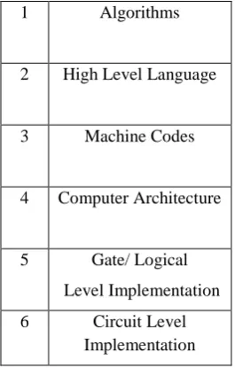
For designing any of the hardware, the designer follows number of steps which are shown in fig.1
1 Algorithms
2 High Level Language
3 Machine Codes
4 Computer Architecture
5 Gate/ Logical
Level Implementation
6 Circuit Level Implementation
Fig. 1 Design Procedure of a digital hardware
The gate/ logical level designing are the design of blocks defined as the micro architecture at the logic gate levels. The last level is the circuit level implementation which is the transistor level design of the basic elements like gate, multiplexers etc.
So, in this paper the authors shows the transistor level/ circuit level implementation of the main logical blocks of the cost-effective reversible programmable logic array by effective structure of CMOS – XOR gate, which is implemented by only 3- transistor. The logical/ gate level implementation of the reversible programmable logic array has been already discussed by the authors in ref. 2
3.
REVESIBLE LOGIC GATE
A logic gate „G‟ is reversible if, for any output there is unique input „A‟, such that applying G (A) = P. If a gate „G‟ is reversible, there is an inverse gate G‟ which maps P to A. for which G (A) = P. So, a reversible gate inputs can be uniquely determined from its outputs. For logical reversibility in the digital logics there are two conditions as follows [2].
Fan-Out is not permitted Feedback is not permitted
There are several reversible logic gates in the literature like Feynman gate (FG), Toffolli gate (TG), Fredkin gate (FRG), Peres gate (PG), New gate (NG, MKG, HNG and TSG, MG) [2]. Here we are reviewing the, Feynman gate and MG (MUX gate) [2] because these gates are the basic gates of the destined structure.
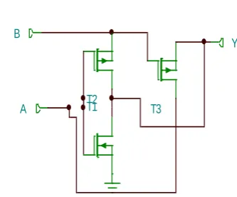
A. Feynman Gate
Fig.2 shows the 2×2 reversible gate called Feynman gate. Feynman gate is also recognized as controlled- not gate (CNOT). It has two inputs (A, B) and two outputs (P, Q). The outputs are defined by P=A, Q=A XOR B .This gate can be used to copy a signal. Since fan-out is not allowed in reversible logic circuits, the Feynman gate is used as the fan-out gate to copy a signal. Quantum cost of a Feynman gate is 1.
Fig.2: 2×2Feynman gate structure
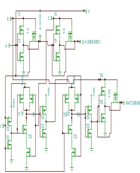
B. MUX Gate
Fig.3 shows the pictorial representation of 3×3 reversible gate called MUX (MG) gate [2]. It is a conservative gate having three inputs (A, B, C) and three outputs (P, Q, R). The outputs are defined by P=A, Q=A XOR B XOR C and R= A‟C XOR AB. The hamming weight of its input vector is same as the hamming weight of its output vector and its Quantum cost is 4.
Fig.3: 3×3 MUX gate
4.
CMOS REALIZTION OF REVERSIBLE GATES
Fig. 4 3-Transistor CMOS Realization of EX-OR gate
Working table of New CMOS EX-OR gate
Input A
Input
B T1 T2 T3 Output
Low Low ON OFF OFF Low
Low High ON OFF OFF High
High Low OFF ON ON High
(Degraded)
High High OFF OFF OFF Low
However when A=1 and B=0, there is a voltage degradation due to threshold drop across transistor T3 resultantly the output Y will also degraded wart input. This degradation can be minimized by increasing the W/L ratio of the T3 [3] because
𝑉𝑇= 𝑉𝑇0 + ᵧ ( 𝑉𝑆𝐵+ ∅0 - ∅0 - 𝛼𝑙 𝑡𝑜𝑥
𝐿 (𝑉𝑆𝐵+ ∅0) - 𝛼𝑣 𝑡𝑜𝑥
𝐿 (𝑉𝐷𝑆) +𝛼𝑤 𝑡𝑜𝑥
𝑊 (𝑉𝑆𝐵+ ∅0) ……….. (1)
Where 𝑉𝑇0 is the zero bias threshold voltage, ᵧ is the bulk threshold coefficient, ∅0 is 2∅𝐹, where ∅𝐹 is the Fermi potential, 𝑡𝑜𝑥 is the thickness of the oxide layer and 𝛼𝑙 , 𝛼𝑣 , 𝛼𝑊 are the process dependent parameters. So, from eq (1) it is clear that by increasing the W it is possible to decrease the threshold voltage and therefore by increasing the width of transistor T3, keeping the length constant, it is possible to
Minimize the voltage degradation due to threshold voltage drop [3].
A. Transistor Implementation of Feynman Gate & MUX gate
The transistor level implementation of the Feynman gate and the MUX gate is shown in fig. 5 & fig.6. This implementation uses the novel 3- transistor xor gate structure to make the circuit less complex and also having less delay due to the less critical paths. The AND structure of CMOS transistor s same as we studied in the literatures.
T1 T2
T3
Y B
Fig.5 Transistor Implementation of Feynman Gate by 3- Transistor EX-OR gate
Fig. 6 Transistor Implementation of MUX Gate by 3- Transistor EX-OR gate
5.
RESULT & DISCUSSION
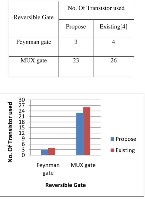
The CMOS realization of the main logic blocks of the reversible programmable logic array has been proposed. This work proposes the effective design of CMOS MUX gate & CMOS Feynman gate by using novel 3 transistor based EX-OR gate. The transistor count in the proposed design is less than the existing design methodology [4]. In the proposed design of current work the numbers of transistors used are 3 for Feynman gate & 23 for MUX gate. However the existing approach provides 4 transistors for Feynman gate & 26 for MUX gate can be seen in the table 2.
T1 T2 T3 Q B A P V d d V d d V d d V d d V d d T1 T2 T3 T4 T5 T6
T7T9 T8
T10 T11 T12 A A B A X O R B C
Q= A XOR B XOR C
T13
T14 T18T20 T19
T21 T22 T23 T24 T25 T 2 6
Table 2 Comparison of Two Design Methodologies
Reversible Gate
No. Of Transistor used
Propose Existing[4]
Feynman gate 3 4
MUX gate 23 26
Fig. 7 Comparison of Proposed & Existing Design
As we can see the results in the table, the number of transistor used in the reversible gates are less as compare to the existing design. So, this proposed structure of Novel 3- transistor XOR gate is better for realizations of reversible circuits at circuit level implementation for the low power industrial applications.
6.
REFERENCES
[1] R.Landauer, “ Irreversibility and heat generation in the computational process” , IBM J. Res. Develop, Vol. 5, pp. 183-191,1961
[2] Pradeep Singla and Naveen Kr. Malik, “ A cost- effective design of reversible programmable logic array” , International Journal of Computer applications Vol.41(15), pp.41-46, 2012.
[3] Shubhajit Roy et al. “ a high Speed 8 transistor full adder design using noval 3 transistor XOR gate”, world accadmy of science and technology, pp 760-766, 2008.
[4] D.P.Vasudevan et al. , : CMOS realization of online Testable reversible logic gates” proceedings of the IEEE computer society annual symposium on VLSI, 0-7695-2365-X/5.R. E. Sorace, V. S. Reinhardt, and S. A. Vaughn, “High-speed digital-to-RF converter,” U.S. Patent 5 668 842, Sept. 16, 1997.
[5] H.T. Bui, Y. Wang, Y. Jiang , “Design and analysis of 10-transistor full adders using novel XOR–XNOR gates,” in Proc. 5th Int. Conf. Signal Process., vol. 1, Aug. 21–25, 2000, pp. 619–622.
0 3 6 9 12 15 18 21 24 27 30
Feynman gate
MUX gate
No
. O
f
Tra
ns
ist
o
r
us
ed
Reversible Gate
Propose