Measuring the Local Twist Angle and Layer Arrangement
in Van der Waals Heterostructures
Tobias A. de Jong,* Johannes Jobst, Hyobin Yoo, Eugene E. Krasovskii, Philip Kim,
and Sense Jan van der Molen
The properties of Van der Waals (VdW) heterostructures are determined by the twist angle and the interface between adjacent layers as well as their polytype and stacking. Here, the use of spectroscopic low energy electron microscopy (LEEM) and micro low energy electron diffraction (mLEED) methods to measure these properties locally is described. The authors present results on a MoS2/hBN heterostructure, but the methods are
applicable to other materials. Diffraction spot analysis is used to assess the benefits of using hBN as a substrate. In addition, by making use of the broken rotational symmetry of the lattice, the cleaving history of the MoS2
flake is determined, that is, which layer stems from where in the bulk.
1. Introduction
The list of materials that can be thinned down to single layers has been vastly extended since the first isolation of graphene monolayers in 2004.[1]In the few layer limit these so-called Van der Waals (VdW) materials exhibit properties that are vastly
different from their bulk counterparts, and they are hence interesting for fundamental research and applications alike.[2]In
partic-ular the combination of different VdW materials into heterostacks has the poten-tial for a wide range of applications.[3]
Mechanical exfoliation of single layers and their subsequent combination via stamping techniques makes creation of heterostacks of (almost) arbitrary layer arrangements possi-ble. These methods have now advanced to the point that regular fabrication of multilayer heterostacks with sufficiently low defect density is commonplace.
The quality and properties of these heterostacks, however, are not only infl u-enced by defects, but also critically depend on other factors such as the substrate, the crystallographic polytype of the layers, and their relative orientation with respect to each other. In particular, atomically flat substrates that do not perturb the electronic structure of the VdW stacks are desired, and consequently hexagonal boron nitride is widely used.[4,5] The polytype of the
different flakes, that is, the different crystallographic confi gu-rations of the layers with respect to each other, determines many of the properties of VdW heterostacks. This applies in particular to transition metal dichalcogenides (TMDs) that can, for example, be semiconductors or metals depending on their polytype.[6] Interlayer twist can cause stacking defects and strain, which can either result in a reduction of sample quality or in desired Moire reconstructions. These reconstructions can strongly alter proper-ties of the stacks such as their band structure[7,8]or cause correlated electron effects culminating in the recent discovery of supercon-ductivity in magic-angle bilayer graphene.[9]
In order to understand the properties of complex hetero-structures, characterization techniques are needed to study the
flatness of the interface, the relative rotation of the layers, and their polytype. Moreover, these techniques need to find the micrometer-sized heterostacks on millimeter-sized samples and simultaneously have sufficient lateral resolution to study details on the sub-micrometer length scale.
Typical characterization methods include, among others, optical microscopy, scanning electron microscopy (SEM), and atomic force microscopy (AFM) to obtain information about topography and thickness, Raman spectroscopy and angle-resolved photoemission spectroscopy (ARPES) for layer number and vibronic and electronic structure, respectively. Moreover, scanning tunneling microscopy (STM) and transmission electron microscopy (TEM) techniques allow advanced
T. A. de Jong, Dr. J. Jobst, Prof. S. J. van der Molen Leiden Institute of Physics
Leiden University
Niels Bohrweg 2, P.O. Box 9504, NL-2300 RA Leiden, The Netherlands E-mail: [email protected]
Dr. H. Yoo, Prof. P. Kim Department of Physics Harvard University MA 02138, USA Prof. E. E. Krasovskii
Departamento de Física de Materiales Universidad del País Vasco UPV/EHU 20080 San Sebastián/Donostia, Spain Prof. E. E. Krasovskii
Donostia International Physics Center (DIPC)
Paseo de Manuel Lardizabal 4, 20018 San Sebastián/Donostia, Spain Prof. E. E. Krasovskii
IKERBASQUE
Basque Foundation for Science E-48013 Bilbao, Spain
The ORCID identification number(s) for the author(s) of this article can be found under https://doi.org/10.1002/pssb.201800191.
© 2018 The Authors. Published by WILEY-VCH Verlag GmbH & Co. KGaA, Weinheim. This is an open access article under the terms of the Creative Commons Attribution License, which permits use, distribution and reproduction in any medium, provided the original work is properly cited.
DOI: 10.1002/pssb.201800191
characterization down to the atomic level. Although all these methods yield detailed insights into specific aspects of VdW heterostructures, they either can not simultaneously obtain information on flatness, layer number, rotation angle, and polytype or need very specific sample preparation, for example, free-standing samples for TEM investigations.
In this work, we demonstrate that all these parameters can conveniently be obtained within one setup using low-energy electron microscopy (LEEM) and diffraction (LEED). We study a VdW heterostack of molybdenum disulfide (MoS2) monolayer,
bilayer, and trilayer on bulk hexagonal boron nitride (hBN). This is a widely used material combination, but the methods demonstrated can be applied to virtually any heterostack on a large variety of substrates. We deduceflatness, layer number, and polytype from spectroscopic LEEM measurements.
For the TMD MoS2, there are three polytypes known, designated
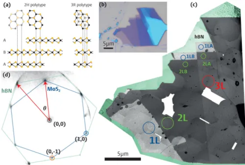
1T, 2H, and 3R. In this classification, the number reflects the number of layers in the unit cell, and the letter indicates whether the unit cell is hexagonal (H), rhombohedral (R), or trigonal (face-centered cubic, T). The unit cell of the naturally most abundant, semiconducting 2H polytype consists of two layers of covalently bonded atoms (see Figure 1a), which are weakly bonded by interlayer VdW force. In this polytype, subsequent layers are rotated 60with respect to each other. Contrary to a simple hexagonal lattice such as graphene, which is sixfold symmetric, here a single VdW layer is threefold rotation symmetric (symmetry groupD3h), that is,
a rotation over 120does not change the lattice. Hence, there are precisely two distinct types of layers in the 2H polytype, as an even number of rotations of 60yields a total rotation corresponding to the symmetry of a single layer. This is in contrast to the 1Tstacking, where all layers are identical, albeit different from the other
polytypes, and the 3R stacking, where all layers have the same orientation, but lattice sites are shifted (as shown in Figure 1a). As the translation symmetry is purely defined by the shape of the unit cell, the reciprocal lattice is trigonal. Due to the threefold symmetry, the sixfirst order diffraction spots are split in two equivalence classes, commonly denotedKandK0. In the following, we use the fact that these equivalence classes are visible in the observed LEED patterns and only consider the 2H and 3R polytypes.
2. Experimental Section
2.1. Experimental
The VdW heterostack was fabricated through mechanical exfoliation and stamping: The MoS2flake was exfoliated using
scotch tape onto silicon oxide for thickness determination and picked up again. Subsequently it was used to pick up a bottom hBN flake and transferred onto a silicon nitride substrate. Afterwards it was annealed at 350C to remove polymer residue. In LEEM, the sample is in ultra high vacuum and reheated to the same temperature. At this elevated temperature surface contamination by hydrocarbon deposition is prevented. It is then illuminated with electrons of energies between 0 and 60 eV. This landing energy E0 can be tuned precisely by changing a
decelerating electric field between objective lens and sam-ple.[10,11]An image is formed from the reflected electrons, either
in real space (LEEM image) or in reciprocal space (LEED pattern). This combination of real space andk-space information and the ability to rapidly switch between the two, forms one of the strengths of LEEM instruments.
Figure 1. a) Top view and side view of the atomic structure of the 2H and 3R polytypes of MoS2. b) Optical microscope image of the MoS2flake on SiO before transfer, showing a clear layer contrast between different layer counts. c) Overview of the MoS2flake composed of 90 bright-field LEEM micrographs. The MoS2flake shows different intensities, the surrounding hBN substrate is shaded green for clarity. Indicated are the areas studied with
In this work, we use the SPECS P90 based ESCHER LEEM. This setup is aberration correcting, enabling a maximum resolution of 1.4 nm.[12]In these experiments images are taken with a 5mmfield of view. Larger images are created either in photoemission electron microscopy (PEEM) mode or by stitching multiple LEEM images together.
By scanning the electron energyE0and taking an image for
each energy, spectroscopic data can be obtained. This can be done both in real space as well as in diffraction. Spectroscopic mLEED measurements are performed by limiting the illumi-nated area using an aperture and taking diffraction images for a range of landing energies. This allows study of small areas of homogeneous layer number, tofingerprint the material, and to determine layer number.[13,14] In this work, spectra are determined by averaging, for each energy separately, over an area in k-space around the respective diffraction spot, as indicated in Figure 1d. The data was corrected for detector effects and no smoothing of curves was performed.
The shape of the diffraction spots reveals additional information, for example, the width of the central (0,0) spot (the specularly reflected electrons) is a measure for sample roughness.[15] For determination of the spotwidth, a linecut along the maximum of the central peak and perpendicular to the dispersive direction of the prisms was taken, after the data was corrected for detector effects. The full width half maximum (FWHM) of a Gaussianfit to the top of this peak is then used as indicator for the sampleflatness.
2.2. Computational
The reflection spectra for specular and diffracted beams were calculated for different layer counts of 2H-MoS2using an ab
initio theory of electron diffraction.[16] The calculations are performed with a full-potential linear augmented plane waves method with a self-consistent crystal potential obtained within the local density approximation as presented in ref. [17]. The reflectivity spectra are obtained with the all-electron Bloch-wave-based scattering method of ref. [18], properly modified for stand-alone two-dimensionalfilms offinite thickness.[19]The inelastic scattering was taken into account by introducing the optical potential: the imaginary potentialiViis taken to be spatially constant over afinite slab (where the electron density is non-negligible) and to be zero in the two semi-infinite vacuum half-spaces. We used the energy dependenceVi(E) that was calculated
in ref. [20] for a similar substance, WSe2, within the GW
approximation. Spectra were shifted by4.0 eV to account for the unknown work-function and substrate doping.
3. Results and Discussion
3.1. Imaging and Twist Angle Determination
A thin MoS2flake that contains monolayer, bilayer, and trilayer
areas was identified after exfoliation onto a Si/SiO2substrate.
The layer number is clearly visible as different shades of purple in the optical microscopy image in Figure 1b. After stacking it onto a hBNflake and transferring the heterostructure to thefinal
silicon nitride substrate (see section 2), PEEM mode is used in the LEEM setup to identify theflake. In the following, only LEEM data is discussed.
The entire heterostack is too big to be imaged in one LEEM
field of view. Consequently, Figure 1c shows an overview that is stitched together from 90 individual LEEM images (the white spots are areas of missing images). This LEEM overview reveals the features already visible in the optical image in much greater detail: a large monolayer (brightest), bilayer (darkest), and trilayer (intermediate gray) areas, as well as a region with smaller, rectangular monolayer, and bilayer areas in the top right surrounded by the hBN (shaded green for clarity).
In order to determine the angle between the MoS2and the
hBN crystal, we perform LEED experiments where both materials are illuminated simultaneously by the electron beam. A LEED pattern taken on the edge of the flake is shown in Figure 1d. Here, 50 images taken at even intervals in the 50– 60 eV range were averaged to enhance the signal-to-noise ratio and to capture all features. Two distinct hexagonal diffraction patterns are visible. The distance between the central (0,0) beam of specularly reflected electrons and the diffraction spots is inversely proportional to the lattice constant. Consequently, we can identify the diffraction spots further out as stemming from hBN and the ones further in as stemming from MoS2. The twist
angleθbetween hBN and MoS2diffraction spots, corresponds
directly to the twist angle between the two materials. From Figure 1d we determineθ¼292.
3.2.mLEED Spectroscopy
mLEED measurements were performed for large areas of monolayer (“1L”), bilayer (“2L”), and trilayer (“3L”) MoS2 (the
precise areas as limited by an illumination aperture are indicated in Figure 1c). The FWHM of the (0,0) spot at 32.0 eV, indicative of
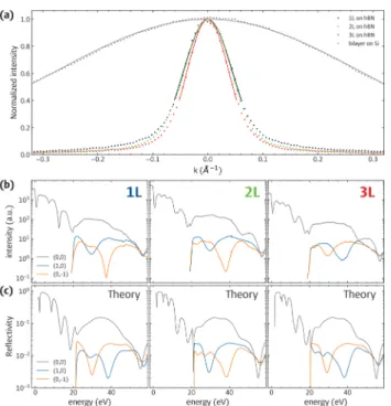
flatness, was determined byfitting the spot profile (see section 2). The profiles and resultingfits are shown inFigure 2a for the mono-(blue), bi- (green), and trilayer (red) areas, resulting in FWHM values of respectively 0.107 A1, 0.104 A1, and 0.091 A1. This is a factor of six lower than values for exfoliated MoS2on a silicon
substrate (gray curve in Figure 2a, 0.66 A1). This large linewidth, due to the roughness of SiO2, confirms thefindings of Yeh et al.[21]
In contrast to their results, wefind no significant broadening of the monolayer peak, indicating that the VdW force between the atomicallyflat hBN and MoS2effectively prevents buckling of the
latter. Combined, this reaffirms the significance of hBN as an atomicallyflat substrate for few layer VdW devices.
Varying the energy and plotting the intensity of the specular and refracted beams as a function of energy results in the spectra shown in Figure 2b. Besides the lattice symmetry, lattice constants, and angle between the layers, which can all be extracted from LEED images, these LEED spectra yield additional information. The specular spectra reflect the density of states of the material.[5,22]The diffracted beams, in addition, contain information about the symmetry properties of the material studied.
The threefold symmetry of the atomic lattice and inequiva-lence of K and K0 for MoS2 is visible in experimental LEED
120angles from each other, dim out. Consequently, we choose one representative spot forKandK0each. They are denoted with their reciprocal lattice coordinates (1,0) and (0,1), as indicated in Figure 1d.
The experimental spectra for the specular spot show a well-defined structure. Differences between different layer counts are however subtle, the most prominent being the minimum at 5.2 eV exhibited by multilayers, but not by the monolayer. For comparison, we performed ab initio calculations of LEED reflectivity spectra for freestanding few layers 2H-MoS2. The
results from these calculations match very well with the experimental data and are shown together in Figure 2c.
The calculated spectra show two classes of diffracted beams: the diffraction spots of the two equivalence classes have different intensities as a function of landing energy, with a pronounced dip at either 29 eV or 38 eV. The experimental diffracted beams reproduce this behavior almost perfectly, with indeed minima at either 29 eV or 38 eV. A feature of the measurement not reproduced in the theoretical spectra is the increasing depth of the minimum at 38 eV for decreasing layer number. We expect this to be due to the presence of the hBN substrate, which is not considered in the calculations.
The difference between spectra from the (1,0) and (0,1) diffracted beams is a result of the fact that the two layer types in
2H stacking are rotated 60 with respect to each other (see Figure 1a). Consequently, looking at the one or the other type of layer should interchange the behavior of theKandK0spots. In fact, as more layers are added on top in the calculations, the diffracted beams interchange behavior for each added layer, as expected from imaging layers of the different types. Therefore, we conclude that the spectra from the first order beams are dominated by the top layer.
In the experimental curves (Figure 2b), the spectra do not interchange from the monolayer to the bilayer case. This difference could have two causes as can be deduced from Figure 1a: The bilayer could either be of the 3R polytype, where both layers have the same orientation, or the layers are in 2H stacking but the second layer is added below the monolayer. The excellent match between experimental data and ab initio calculations does suggest 2H stacking for all areas. However, to fully rule out the presence of 3R stacking we perform additional experiments.
Further spectra, shown inFigure 3a, taken on smaller bilayer and monolayer areas (indicated in the top part of Figure 1c), give additional evidence that the wholeflake is 2H-stacked: As the
flake is continuous, the spectrum inversion, where the diffraction spots switch equivalence class going from a monolayer to an adjacent bilayer area, proves the layers in the sample are 2H-stacked. The fact that the asymmetry remains for
Figure 3. a)mLEED spectra of smaller neighboring areas, indicated in Figure 1c. For the different areas of the same layer count, equivalence classes of first order diffraction spots invert, indicating the top layers in the different areas stem from different layers in the bulk 2H crystal. b) Cartoon showing a reconstruction of which areas stem from which layers in the original bulk crystal as concluded from (a) and and Figure 2b. c) False color image indicating the top layer orientation as can be concluded from the spectra in (a).
the bilayer is thus not due to 3R stacking, but fully due to the low penetration depth of the low energy electrons, causing the spectra to be dominated by the topmost layer.
This notion now also helps to explain the diffracted curves for
“1L”and“2L”in Figure 2b: contrary to the simulation the top layer here stays the same, the additional layer instead being added between the top layer and the substrate.
The fact that we can now determine the rotational type of the top layer, allows us to assign from which layer orientation in the bulk 2H-MoS2the top layer originates for different areas on the
sample. With the additionalmLEED measurements on smaller areas, we thus reconstruct the full cleaving history of the different layers of the MoS2flake in Figure 3b, determining for
each boundary whether a layer is added/subtracted on top of the
flake or on the bottom, information to the best of our knowledge not measurable by any other technique.
4. Conclusions
In conclusion, we have shown the application of spectroscopic LEEM techniques to the characterization of VdW heterostacks. The combination of real space imaging and local electron diffraction enables analysis of sample quality, stacking angle, and polytype within one instrument, without the need for special substrates. We conclude from the significantly reduced diffrac-tion spot width compared to MoS2layers on a silicon substrate,
that the use of hBN as a substrate yields very high sample quality. We compare experimental data with ab initio calculations, which allows us to locally distinguish the orientational type of the top layer and thus to conclude for each boundary of layer count whether a layer is added on top or on the bottom.
Acknowledgements
The authors thank Ruud M. Tromp for the fruitful discussions and useful advice. Furthermore the authors thank Marcel Hesselberth and Douwe Scholma for their indispensable technical support. This work was supported by the Netherlands Organisation for Scientific Research (NWO/OCW) via theVENIgrant (680-47-447, J.J.), as part of the Frontiers of Nanoscience program and by the Spanish Ministry of Economy and Competitiveness MINECO, Grant No. FIS2016-76617-P. H.Y. and P.K. acknowledge the support from ARO MURI (W911NF-14-1-0247).
Conflict of Interest
The authors declare no conflict of interest.
Keywords
heterostacks, LEEM, low-energy electron microscopy, twist, van der Waals materials
Received: April 27, 2018 Revised: July 19, 2018 Published online:
[1] K. S. Novoselov, A. K. Geim, S. V. Morozov, D. Jiang, Y. Zhang, S. V. Dubonos, I. V. Grigorieva, A. A. Firsov,Science2004,306, 666.
[2] K. Novoselov, A. Mishchenko, A. Carvalho, A. C. Neto,Science2016,
353, aac9439.
[3] A. K. Geim, I. V. Grigorieva,Nature2013,499, 419.
[4] I. Meric, C. R. Dean, N. Petrone, L. Wang, J. Hone, P. Kim, K. L. Shepard,Proc. IEEE2013,101, 1609.
[5] J. Jobst, A. J. Van Der Torren, E. E. Krasovskii, J. Balgley, C. R. Dean, R. M. Tromp, S. J. Van Der Molen,Nat. Commun.2016,7, 13621. [6] A. Nourbakhsh, A. Zubair, R. N. Sajjad, K. G. Amir Tavakkoli, W. Chen, S. Fang, X. Ling, J. Kong, M. S. Dresselhaus, E. Kaxiras, K. K. Berggren, D. Antoniadis, T. Palacios,Nano Lett.2016,16, 7798. [7] B. Pamuk, J. Baima, F. Mauri, M. Calandra,Phys. Rev. B2017,95,
075422.
[8] P. C. Yeh, W. Jin, N. Zaki, J. Kunstmann, D. Chenet, G. Arefe, J. T. Sadowski, J. I. Dadap, P. Sutter, J. Hone, R. M. Osgood Jr.,Nano Lett.2016,16, 953.
[9] Y. Cao, V. Fatemi, S. Fang, K. Watanabe, T. Taniguchi, E. Kaxiras, P. Jarillo-Herrero,Nature2018,556, 43.
[10] R. Tromp, J. Hannon, A. Ellis, W. Wan, A. Berghaus, O. Schaff,
Ultramicroscopy2010,110, 852.
[11] R. Tromp, J. Hannon, W. Wan, A. Berghaus, O. Schaff, Ultra-microscopy2013,127, 25.
[12] S. Schramm, J. Kautz, A. Berghaus, O. Schaff, R. M. Tromp, S. J. van der Molen,IBM J. Res. Dev.2011,55, 1.
[13] H. Hibino, H. Kageshima, F. Maeda, M. Nagase, Y. Kobayashi, H. Yamaguchi,Phys. Rev. B2008,77, 075413.
[14] S. C. de la Barrera, Y. C. Lin, S. M. Eichfeld, J. A. Robinson, Q. Gao, M. Widom, R. M. Feenstra,J. Vacuum Sci. Technol. B, Nanotechnol. Microelectron.2016,34, 04J106.
[15] A. Locatelli, K. R. Knox, D. Cvetko, T. O. Mentes, M. A. Nino, S. Wang, M. B. Yilmaz, P. Kim, R. M. Osgood Jr, A. Morgante,ACS Nano2010,
4, 4879.
[16] J. I. Flege, E. E. Krasovskii,Phys. Status Solidi RRL–Rapid Res. Lett.
2014,8, 463.
[17] E. E. Krasovskii, F. Starrost, W. Schattke, Phys. Rev. B1999, 59, 10504.
[18] E. E. Krasovskii,Phys. Rev. B2004,70, 245322.
[19] V. U. Nazarov, E. E. Krasovskii, V. M. Silkin,Phys. Rev. B2013,87, 041405.
[20] F. Siek, S. Neb, P. Bartz, M. Hensen, C. Struber, S. Fiechter, M. Torrent-Sucarrat, V. M. Silkin, E. E. Krasovskii, N. M. Kabachnik, S. Fritzsche, R. D. Muino, P. M. Echenique, A. K. Kazansky, N. M̈uller, W. Pfeiffer, U. Heinzmann,Science2017,357, 1274.
[21] P. C. Yeh, W. Jin, N. Zaki, D. Zhang, J. T. Sadowski, A. Al-Mahboob, A. M. van Der Zande, D. A. Chenet, J. I. Dadap, I. P. Herman, P. Sutter, J. Hone, R. M. Osgood Jr.,Phys. Rev. B2014,89, 155408. [22] J. Jobst, J. Kautz, D. Geelen, R. M. Tromp, S. J. Van Der Molen,Nat.