http://www.scirp.org/journal/jpee ISSN Online: 2327-5901 ISSN Print: 2327-588X
DOI: 10.4236/jpee.2017.58001 Jul. 27, 2017 1 Journal of Power and Energy Engineering
Design of Grid-Connected Photovoltaic System
Naseer Khan
1, Muhammad Aamir
2, Faisal Mehmood
3, Muhammad Aslam
1, Muhammad Arif
31Department of Electrical Engineering, UET, Peshawar, Pakistan
2Department of Electrical Engineering, University of Malaya, Malaya, Malaysia
3Department of Electrical Engineering, COMSATS, Abbottabad, Pakistan
Abstract
This paper presents a grid connected photovoltaic system (PV) with a pro-posed high voltage conversion ratio DC-DC converter which steps up the va-riable low input voltages of photovoltaic module to the required DC link tage. This voltage is applied to an H-bridge inverter which converts DC vol-tage into AC volvol-tage and a low pass filter is used to filter the output. By ad-justing the duty ratio of switches in DC-DC converter, the magnitude of in-verter’s output voltage is controlled. The frequency and phase synchroniza-tion are ensured by a feedback signal taken from the grid. In this way, inverter is synchronized and connected with the grid to meet the energy demand. The PV system has been designed and simulated.
Keywords
Photovoltaic Systems (PV), High Voltage Gain, DC-DC Converter, PWM, Inverter, Synchronization
1. Introduction
The demand of electric power is on rise and is anticipated to increase exponen-tially in future. Among main sources of energy, thermal sources such as fossil fuels contribute to bulk amount of power generation. But these fuels are expen-sive due to their bulky demand around the world. Also their reserves are limited and running short. Besides this, their combustion generates pollutants gases which affect the environment in various forms. Due to these factors, the renewa-ble sources of energy are getting attention and the photovoltaic systems (PV) are also becoming more prominent during the last few decades. The photovoltaic module provides a low DC voltage with wide range according to various
operat-How to cite this paper: Khan, N., Aamir, M., Mehmood, F., Aslam, M. and Arif, M. (2017) Design of Grid-Connected Photo-voltaic System. Journal of Power and Energy Engineering, 5, 1-12.
https://doi.org/10.4236/jpee.2017.58001
Received: June 14, 2017 Accepted: July 24, 2017 Published: July 27, 2017
Copyright © 2017 by authors and Scientific Research Publishing Inc. This work is licensed under the Creative Commons Attribution International License (CC BY 4.0).
DOI: 10.4236/jpee.2017.58001 2 Journal of Power and Energy Engineering
ing conditions [1] [2]. A boost converter is required to step up this low DC vol-tage to the required DC link volvol-tage. The conventional boost converters cannot offer such a high voltage gain. Even in case of extreme duty ratio, the conversion efficiency is declined due to losses. This also increases the ratings of devices like output diode and other issues such as severe electromagnetic interference and reverse recovery [3]. The quadrature converters also offer a high voltage gain, but these have equal voltage stress across the switch [4] [5]. In particular cases, the line frequency transformer can also be used, but it increases the size and weight of photovoltaic system [6] [7]. The grid-connected photovoltaic systems also need the inverters for power conversion, grid interconnection and control optimization [8] [9]. Pulse width modulation (PWM) voltage source inverters are most commonly used in PV systems to invert DC voltage into AC before feeding to the grid or AC loads. The connection of inverters to the grid specifi-cally is dependent on the control scheme which is adopted by these inverters. Different control schemes have been under research for grid-connected inverters in the past decade [10] [11]. The phase locked loop technique is being the con-ventional. There are other PLL based grid synchronization techniques like power based PLL, quadrature PLL (QPLL). A PLL based new technique for synchroni-zation with the grid has also been developed in [12].
This paper describes grid-connected photovoltaic system with a proposed high voltage conversion ratio DC-DC converter. This system mainly includes two processing stages: a high voltage conversion ratio converter which converts low DC PV module voltage into the required DC link voltage. The second stage is the inverter which converts it into AC voltage. A low pass filter is designed to filter the inverter output before it is applied to the grid. The DC-DC converter is capable of maintaining the magnitude of inverter’s output voltage and inverter guarantees the phase and frequency synchronization of its output. The proposed system finds applications not only in low power, but can also be extended to some extent to large scale allowing the parallel operation of PV modules.
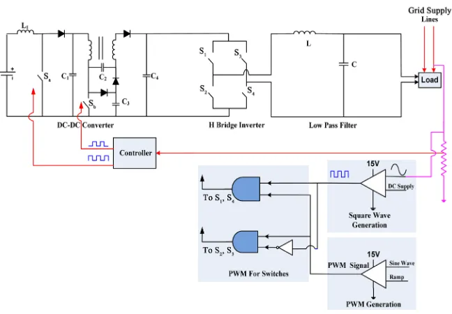
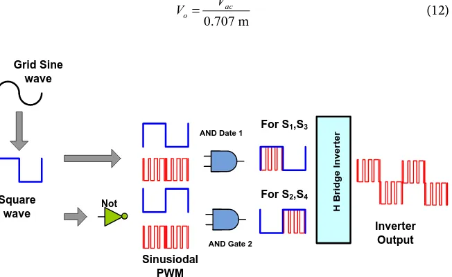
The grid-connected system is shown in Figure 1 with the main constituents as proposed topology of DC-DC converter, inverter and a low-pass filter. As the PV module normally generates low voltage, so a boost converter is needed to step up this DC voltage to a higher value. This output of DC-DC converter is applied to an H-bridge inverter which has four MOSFET switches S1 to S4. The discrete
pairs of switches (S1, S4) and (S2, S3) are operated to produce positive and
nega-tive half cycles of AC voltage respecnega-tively. For the operation of inverter, the pulse width modulation method is used in which a sinusoidal pulse width mod-ulated signal is achieved by the comparison of a sine wave and saw-tooth wave. This sinusoidal PWM signal is then compared with a square wave to get driving signals for the switches (S1, S4). Similarly, the sinusoidal PWM signal is
com-pared with inverted square wave to get driving signals for the switches (S2, S3).
DOI: 10.4236/jpee.2017.58001 3 Journal of Power and Energy Engineering Figure 1. The grid-connected system.
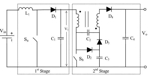
2. Operation of the Proposed Conveter
The proposed converter is shown in Figure 2 which includes two stages. An in-ductor L1, capacitor C1, switch Sa and diode D1 constitute the first stage. A
coupled inductor and capacitors C2, C3 and C4 form the second stage. Switches Sa
and Sb are used to control the operation of first and second stage respectively.
2.1. Operation of First Stage
When switch Sa is turned on, L1 inductor is storing the energy. During this
mode, diode D1 is reverse biased and capacitor C1 supplies current to the second
stage which acts as a load. When switch Sa is turned off, diode D1 becomes on
and the current iL flows through the load and capacitor C1. These operating
modes are shown in Figure 3.
The voltage conversion ratio of first stage is same as boost converter and is given by
1
in 1
1 1 V
V = −d (1)
where V1, Vin and d1 are the output voltage, input voltage and duty ratio of first stage respectively.
2.2. Operation of Second Stage
Figure 4 shows the second stage of the proposed topology. In order to accom-plish mode analysis of second stage converter, coupled inductor is displayed as Lm (magnetizing inductance), leakage inductances Lk1 and Lk2 on the primary
DOI: 10.4236/jpee.2017.58001 4 Journal of Power and Energy Engineering Figure 2. Proposed DC-DC converter.
Figure 3. Topologies of first stage (a) Sa is on (b) Sa is off.
Figure 4. Second Stage of proposed converter.
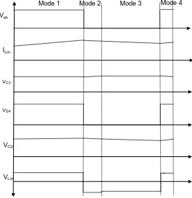
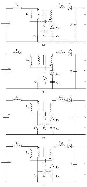
second stage are shown in Figure 5. This stage as shown in Figure 6 can be ana-lyzed in four operating modes.
Mode 1: The switch Sb is initially turned on as shown in Figure 6(a). D2
be-comes reverse biased and the applied voltage causes the current on primary side to increase. In this mode, the current flowing through secondary winding is zero and there is increase in energy on the primary side.
C1
L1
C2
C3
C4
1st Stage 2nd Stage
Sa
Sb
Vin V
o
D1
D3
D4
D2
V1
C1
L1
1st Stage
.
.
iL.
io
iC D1
Sa Vin
C1
L1
1st Stage
.
.
iL io
D1
Sa
Vin
Lk1
C2
C3
C4
2nd Stage Lm
Lk2
+
Vo
_
D2
D3
D4
DOI: 10.4236/jpee.2017.58001 5 Journal of Power and Energy Engineering Figure 5. Steady state waveforms of the second stage.
Mode 2: In second mode, switch Sb is turned off and diode D2 is forward
bi-ased which charges capacitor C3. The secondary winding is also receiving some
of primary current via capacitor C2 during this mode. The energy in magnetizing
inductance decreases and there is increase in secondary current. Diode D3
re-mains in off condition. Capacitor C3 becomes charged at the end of this mode.
Mode 3: In this mode, switch Sb remains off and D2 becomes reverse biased.
Primary, secondary windings and capacitor C2 are series connected across the
source. This allows the direct transfer of energy to the output from capacitor C2,
coupled inductor and source.
Mode 4: The switch Sb is turned on and current on the primary side starts
in-creasing there by storing energy in magnetizing inductance. Diode D3 becomes
forward biased and capacitor C2 is charged by capacitor C3. The current on
sec-ondary winding decays to zero and D4 becomes reverse biased. The voltage
across C3 becomes equal to the voltage across C3 causing diode D3 to become
re-verse biased at the end of forth mode and the circuit proceeds to its initial condi-tion.
Some assumptions are made for the derivation of voltage conversion ratio. The coupling co-efficient of coupled inductor is unity and the diodes are ideal. Let VLm, VL2, V1 and Vo represent the voltages across magnetizing
induc-tance, secondary winding, input and output of second stage respectively. d2 is the duty ratio of second stage.
During on and off modes the inductor Lm voltage is respectively given by:
Vsb
ILm
VC3
VLm
VC2
VD4
DOI: 10.4236/jpee.2017.58001 6 Journal of Power and Energy Engineering
(a)
(b)
(c)
[image:6.595.223.522.61.707.2](d)
Figure 6. Topologies of second stage (a) Mode 1; (b) Mode 2; (c) Mode 3; (d) Mode 4. Lk1
Lm
Lk2
Sb
C2
D2
D3
D4
C3
C4
+
Vo
_
Lk1
Lm
Lk2
Sb
C2
D2
D3
D4
C3
C4
+
Vo
_
Lk1
Lm
Lk2
Sb
C2
D2
D3
D4
C3
C4
+
Vo
_
Lk1
Lm
Lk2
Sb
C2
D2
D3
D4
C3
C4
+
Vo
DOI: 10.4236/jpee.2017.58001 7 Journal of Power and Energy Engineering
1
Lm
V =V (2)
2 L Lm V V n
= − (3)
Application of inductor volt-second balance to Equation (2) and Equation (3) yields:
2
2 1 2 0
L Lm
V V d V d
n ′ = + − = 2 1 2 2 L nd V V d =
′ (4)
Generally the relation between primary and secondary voltages is given the following equation:
2
L Lm
V =nV (5)
The inductor Lm voltage can be written from Equation (5) in the following
form: 2 1 2 Lm d V V d =
′ (6)
During Mode 2, the voltage across capacitor C3 is given by the following
equa-tion:
3 1
C Lm
V = +V V (7)
Substitution of Equation (6) into Equation (7) leads to the following equation:
3 1 2 1 C V V d′
= (8)
As capacitor C2 is charged by capacitor C3 and at the end of mode 4,
2 3
C C
V =V so
2 3 1
2 1
C C
V V V
d
= =
′ (9)
During Mode 3, apply KVL
1 2 2
o Lm c L
V =V +V +V +V
2 1 1 2 1 1
2 2 2
o
d V V nd V V V
d d d
= + + + ′ ′ ′ 2 1 2 2 o V nd V d + =
′ (10)
This is the voltage gain of second stage and the voltage conversion ratio of proposed topology is obtained by the product of voltage gains of both the stages i.e.; the product of Equation (1) and Equation (10) yields:
(
2)(
2 1)
2
1 1
o
in
V nd
V d d
+ =
− − (11)
ra-DOI: 10.4236/jpee.2017.58001 8 Journal of Power and Energy Engineering
tio n, the required DC link voltage can be achieved at lower values of duty ratios.
3. Grid Connected Inverter
In order to synchronize the phase and frequency of inverter voltage with the grid, a signal is taken as reference from grid voltage. This feedback signal is con-verted into square wave in a comparator as shown in Figure 7. The positive and negative half cycles of the grid voltage appear as high and low voltage respec-tively at the output of the comparator. The rising and falling edges of this wave correspond to the start of positive and negative half cycle of grid sine wave re-spectively. The square wave actually determines the phase and frequency of the output of H-bridge inverter. The comparison of sinusoidal PWM signal for half of the period (10 ms) with same square wave generates gate drive signals for one pair of switches (S1, S4). Similarly the comparison of sinusoidal PWM signal with
inverted square wave for half of the period generates gate drive signals for the other pair of switches (S2, S3). The transition from low to high in square will
make switches S1 and S4 to turn on and S2 and S3 to turn off. Accordingly, the
inverter voltage changes its polarity at exactly the same time as the grid voltage. Any shift in grid voltage is followed by the square wave generated accordingly. The same shift is adopted by the gate drive signals and hence the same shift oc-curs in the output voltage of inverter making it in phase with connected grid.
The inverter in this design operates at constant modulation index (m) and the magnitude of grid voltage and its output voltage should be identical. This is ac-complished by changing the duty ratio of DC-DC converter switches (Sa, Sb) by a
µ-controller. The grid voltage is stepped down by a simple voltage divider circuit and a measured value is given to the µ-controller which reads the input voltage (Vin) of converter and the voltage of grid (Vac). The µ-controller calculates the
desired output voltage (Vo) of DC-DC converter using the grid voltage by the
equation [13].
0.707 m
ac o
V
[image:8.595.214.540.503.703.2]V = (12)
Figure 7. Frequency and phase synchronization.
Square wave
Not
AND Date 1
Sinusiodal PWM
H Bridge Inverter
AND Gate 2
Grid Sine wave
Inverter Output For S1,S3
DOI: 10.4236/jpee.2017.58001 9 Journal of Power and Energy Engineering
Equation (11) is used to compute the duty ratio (d). Ton and Toff are computed
from the duty ratio. The frequency of switching signal is taken to be 20 KHz and two timers are used to produce switching signals of this selected frequency and duty ratio for the operation of DC-DC converter.
4. Simulation Results
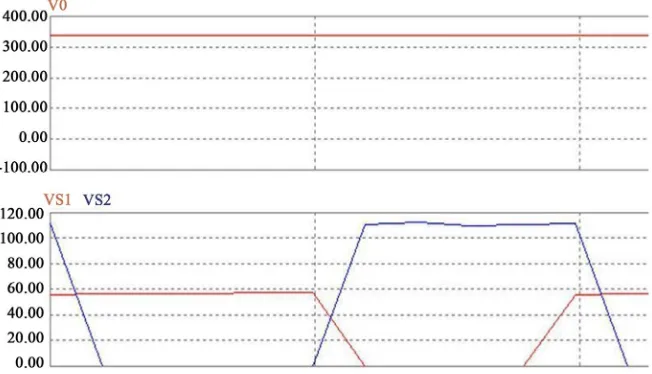
The system specifications and its design parameters are given in Table 1. The proposed topology has been validated by performing its simulation. The results demonstrate a good accordance with the analysis. Figure 8 shows the required voltage of 350 V is achieved at considerable low duty ratio and the output is al-most ripples free. The converter has been simulated for the lowest value of input voltage, Vin = 30 V, still it operates excellently to give the required voltage at low
value of ~0.45. Figure 8 also demonstrates that the proposed converter has less voltage stresses across the switches. The switch Sa has less voltage stress which is
[image:9.595.212.538.313.500.2] [image:9.595.208.539.548.743.2]about 60 V. The voltage stress across Sb is less than 110 V which is far less than
Figure 8. DC-DC converter output.
Table 1. System specifications and parameters.
Specification and parameters Symbols Values
Input voltage Vin 30 - 60 VDC
DC link voltage Vd 350 V
Output voltage Vac 220 V
Frequency f 50 Hz
Power capacity P 500 watt
Boost stage inductance L1 31 µH
Magnetizing inductance Lm 188 µH
Filter inductance L 2.5 mH
DOI: 10.4236/jpee.2017.58001 10 Journal of Power and Energy Engineering
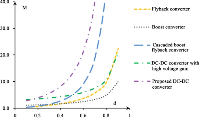
the output voltage (350 V). These less stresses allow the selection of switches in the design procedure to have low voltage ratings. This lowers the cost of the proposed PV system. Comparison has been made been made in Figure 9 among the proposed topology, simple boost, flyback, cascaded boost flyback and anoth-er high voltage gain convanoth-ertanoth-er presented in [14]. This comparison has been made for the same input voltage. The voltage conversion ratio of cascaded boost fly-back convert can be increased by selecting the higher value of turn’s ratio. But this will increase the size of the system. Figure 9 shows that the voltage conver-sion ratio (M) of proposed topology is very high in comparison with the other converters.
The required DC voltage can be achieved at low duty ratio of ~0.4 in the pro-posed converter. The lower value of duty ratio decreases the conduction losses and hence improves the efficiency of the proposed system to some extent. The H-bridge inverter has been also simulated. Figure 10 shows the simulated results of inverter’s output. The output of inverter is square wave and not suitable for most of the applications, so a low pass filter has been designed and simulated. This filter eliminates most of the ripples from the inverter’s output. The output of low pass LC filter is also shown in Figure 11. This simulation result shows that the output voltage is almost sinusoidal having low ripples. This can be used for most of the electrical loads. This output is applied to grid to meet the present day demand of energy.
5. Conclusion
[image:10.595.215.538.512.706.2]This paper proposes the grid-connected photovoltaic system with a proposed topology of DC-DC converter. The converter with a high voltage conversion ra-tio can easily boost up the lower PV voltage to the required DC voltage at low duty ratio. As the gain is high, this allows the parallel operation of PV modules and also eradicates the need of power transformer to achieve the required grid
DOI: 10.4236/jpee.2017.58001 11 Journal of Power and Energy Engineering Figure10. Inverter output voltage.
Figure 11. Inverter output using filter.
voltage. This results in high efficiency and reduced size of this system. The con-verter has low voltage stresses across the switches with decreased cost of the sys-tem. The system is beneficial in terms of unit saving as it can meet the demand of load. It may be implemented for a three-phase system.
References
[1] Chen, Y. and Smedley, K.M. (2004) A Cost-Effective Single-Stage Inverter with Ma- ximum Power Point Tracking. IEEE Transactions on Power Electronics, 19, 1289- 1294. https://doi.org/10.1109/TPEL.2004.833458
[2] Andersen, G.K., Klumpner, C., Kjaer, S.B. and Blaabjerg, F. (2002) A New Green Power Inverter for Fuel Cells. Power Electronics Specialists Conference,2, 727-733. https://doi.org/10.1109/psec.2002.1022540
[3] Mohan, N. and Undeland, T.M. (2007) Power Electronics: Converters, Applications, and Design. John Wiley & Sons, Hoboken.
[4] Maksimovic, D. and Cuk, S. (1991) Switching Converters with Wide DC Conver-sion Range. IEEE Transactions on Power Electronics, 6, 151-157.
https://doi.org/10.1109/63.65013
[5] Maksimovic, D. (1989) Synthesis of PWM and Quasi-Resonant DC-DC Power Con- verters. Doctoral Dissertation, California Institute of Technology, California. [6] Calais, M., Myrzik, J., Spooner, T. and Agelidis, V.G. (2002) Inverters for Single-
Phase Grid Connected Photovoltaic Systems: An Overview. Power Electronics Spe-cialists Conference PESC,4, 1995-2000.
DOI: 10.4236/jpee.2017.58001 12 Journal of Power and Energy Engineering Photovoltaic Modules: A Review. Industry Applications Conference, 2, 782-788. https://doi.org/10.1109/ias.2002.1042648
[8] Kazmierkowski, M.P. and Malesani, L. (1998) Current Control Techniques for Three-Phase Voltage-Source PWM Converters: A Survey. IEEE Transactions on Industrial Electronics, 45, 691-703. https://doi.org/10.1109/41.720325
[9] Kojabadi, H.M., Yu, B., Gadoura, I.A., Chang, L. and Ghribi, M. (2006) A Novel DSP-Based Current-Controlled PWM Strategy for Single Phase Grid Connected Inverters. IEEE Transaction Power Electronics, 21, 985-993.
https://doi.org/10.1109/TPEL.2006.876851
[10] Kjaer, S.B., Pedersen, J.K. and Blaabjerg, F. (2005) A Review of Single-Phase Grid- Connected Inverters for Photovoltaic Modules. IEEE Transactions on Industry Ap-plications, 41, 1292-1306. https://doi.org/10.1109/TIA.2005.853371
[11] Barbosa, P.G., Rolim, L.G.B., Watanabe, E.H. and Hanitsch, R. (1998) Control Stra- tegy for Grid-Connected DC-AC Converters with Load Power Factor Correction.
IEE Proceedings-Generation, Transmission and Distribution, 145, 487-492. https://doi.org/10.1049/ip-gtd:19982174
[12] Jung, H.Y., Ji, Y.H., Won, C.Y., Song, D.Y. and Kim, J.W. (2010) Improved Grid- Synchronization Technique Based on Adaptive Notch Filter. 2010 International Po- wer Electronics Conference (IPEC), Sapporo, 21-24 June 2010, 1494-1498. https://doi.org/10.1109/IPEC.2010.5544516
[13] Singh, M.D. (2008). Power Electronics. Tata McGraw-Hill Education, Pennsylvania Plaza.
[14] Yang, L.S., Liang, T.J. and Chen, J.F. (2009) Transformerless DC-DC Converters with High Step-Up Voltage Gain. IEEE Transactions on Industrial Electronics, 56, 3144-3152. https://doi.org/10.1109/TIE.2009.2022512
Submit or recommend next manuscript to SCIRP and we will provide best service for you:
Accepting pre-submission inquiries through Email, Facebook, LinkedIn, Twitter, etc. A wide selection of journals (inclusive of 9 subjects, more than 200 journals)
Providing 24-hour high-quality service User-friendly online submission system Fair and swift peer-review system
Efficient typesetting and proofreading procedure
Display of the result of downloads and visits, as well as the number of cited articles Maximum dissemination of your research work
Submit your manuscript at: http://papersubmission.scirp.org/