ISSN Print: 2333-9705
DOI: 10.4236/oalib.1104687 Aug. 20, 2018 1 Open Access Library Journal
Structural, Electrical and Optical
Characteristics of Zn
100–x
Cd
x
O Thin Films
Hend Alkhammash
1*, H. Abd El-Ghanny
2, M. M. Abd El-Raheem
21Department of Physics, Faculty of Sciences, Taif University, Taif, Saudi Arabia
2Physics Department, Faculty of Science, Sohag University, Sohag, Egypt
Abstract
Thin films of Zn100−xCdxO with x = 0, 2, 4, 6 and 8 at% were deposited by
electron beam evaporation technique on glass substrates. The structural, opt-ical and electropt-ical properties of Zn100−xCdxO films with x = 4 at% have been
investigated as a function of annealing temperature. Only zinc and cadmium appeared in the as-deposited films, by annealing their oxides found to exist. It was observed that the optical properties, such as transmittance, reflectance, optical band gap, and refractive index of Zn100−xCdx, were strongly affected by
annealing temperature. Other parameters named free carrier concentration, electrical resistivity of the films were studied as a function of annealing tem-perature for 4 at% CdO content. The figure indicates that the best value of annealing temperature is at 450˚C.
Subject Areas
Experimental Physics
Keywords
Zn100−xCdxO, Zinc
1. Introduction
Zinc and cadmium play an important role as alloying elements in many super-conductor and semisuper-conductor alloy properties [1] [2] as well as surface coating and plating process materials. These alloying elements are widely used for sol-dering processes, since many solders may contain Cd because of its low melting point, and also brazing processes, for higher temperatures, should use alloys containing large amounts of Zn. In particular, for lamellar eutectic alloys, Zn and Cd can exhibit some interesting properties. Furthermore, Zn-Cd eutectic
How to cite this paper: Alkhammash, H., El-Ghanny, H.A. and El-Raheem, M.M.A. (2018) Structural, Electrical and Optical Characteristics of Zn100–xCdxO Thin Films. Open Access Library Journal, 5: e4687.
https://doi.org/10.4236/oalib.1104687
Received: May 29, 2018 Accepted: August 17, 2018 Published: August 20, 2018
Copyright © 2018 by authors and Open Access Library Inc.
This work is licensed under the Creative Commons Attribution International License (CC BY 4.0).
DOI: 10.4236/oalib.1104687 2 Open Access Library Journal
alloys have been widely used in many experimental studies [3]-[8], because of their low melting point and their regular lamellar structure.
Transparent conducting oxides (TCOs) are a class of materials that transmit visible radiation and conduct electricity. They find application as transparent electrodes in numerous applications such as photovoltaic, flat panel displays, heat reflective coatings on energy-efficient windows, and electrochromics such as smart mirrors [8] [9] [10] [11]. Zinc Oxide (ZnO) holds considerable interest as an optical transparent materials due to its wide band gap (3.3 ev), its amena-bility to defects or impurity doping and other desirable properties such as low cost and non-toxicity [12]. While pure ZnO films present high values of resistiv-ity [13]. CdO is an n-type semiconductor, with a well-established direct band gap at approximately (2.4 - 2.7 ev) and a poor optical transmittance in the visible spectral region [3]. When compared with ZnO, the transmittance of CdO in the visible region of the spectrum has been reported as rather low. However, cad-mium oxide is characterized by a much lower resistivity. Hence, it could directly combine the optical and electrical properties of an alloy of cadmium and zinc oxides, making it useful for its application in solar cells. This paper reports the preparation of Zn-doped Cd (where x = 0, 2, 4, 6 and 8 at%). The X-ray diffrac-tion analysis, transmittance, optical band gap and electrical resistivity are meas-ured to study the effect of the oxidation temperatures and the Ga-doping level. CdxZn1−xO films have been deposited by sol-gel spin-coating method onto glass
substrates. It was observed that the crystal structure changed from wurtzite (ZnO) to cubic (CdO) structure [14]. Zn0.8Cd0.2O thin films were deposited on
glass substrates at different substrate temperatures (Ts) by the direct current (dc) reactive magnetron sputtering method. Results indicated that all the obtained thin films were of highly (002)-preferred orientation and possessing the hex-agonal wurtzite structure of pure ZnO [15]. The ternary Zn1−xCdO (x: 0 - 1) alloy
thin films were deposited on quartz substrate by the direct current reactive magnetron sputtering method. As x varied from x = 0.0 to 0.5, the Zn1−xCdxO
thin films had a hexagonal wurtzite structure of pure ZnO and (002) preferred orientation. The optical band gap energies of the films were tuned from 3.24 eV at x = 0 to 2.04 eV at x = 0.5 [16]. The optical studies showed that the CdxZn1−xO
thin films have optical transmittance in entire visible region. The resistivity of undoped films was very high and it decreased with addition of cadmium. The gas sensing properties were investigated at optimal temperature of 350˚C for various volatile organic compounds like acetone, ethanol and methanol. The CdxZn1−xO thin films with 10 at% cadmium concentration showed the sensitivity
of 50% for 1 ppm ethanol [17].
DOI: 10.4236/oalib.1104687 3 Open Access Library Journal
side giving rise to a highly conducting channel at the interface [18].
This work focuses on preparing Zn100−xCdxO thin films using e-beam
evapora-tion method for CdO content at 0, 2, 4, 6 and 8 at%. The characterizaevapora-tion, opti-cal and electriopti-cal measurements will be carried out. The figure of merit will be studied as a function of annealing temperature.
2. Experimental Details
2.1. Preparation of the Thin Films
For preparing Zn100−xCdxO (x = 0, 2, 4, 6 and 8 at%) bulk samples, proper
quan-tities of ZnO (99.98% purity) and CdO (99.95% purity) were sealed in an eva-cuated quartz ampoule and heated at 500˚C. Continuous stirring of the melt was carried out to ensure good homogeneity. The melt was then rapidly quenched in ice water. Thin films of the considered ratios were prepared by electron beam evaporation in an Edward’s high vacuum coating unit model 306A under pres-sures of 5 × 10⁻⁶ and 8 × 10⁻⁵ Torr before and during film deposition,
respective-ly. The films were deposited on an ultrasonically cleaned microscopic glasses held at room temperature. The thickness of the films (≈200 nm) was controlled using a digital film thickness monitor model TM 200 Maxtek. The deposition rate was ≈12.5 nm/s and then annealed in air for 1 h.
2.2. Characterization and Optical Measurements of the Thin Films
A Jasco model V-570 (UV-Visible-NIR) double beam Spectrophotometer (with photometric accuracy of ±0.002 - 0.004 Abs. and ±3% Trans.) was employed to record the transmission T and reflection R spectra over the wavelength range from 200 to 2500 nm at normal incidence. The absorption coefficient α of the films was determined directly from the spectrophotometer readings using the formula [19]:
2.303log10 1 R
d T
α
= − (1)
where d is the film thickness, T is the transmittance and R is the reflectance of the film.
The optical energy band gap Eg was estimated from the optical measurements
by analyzing the optical data with the expression for the optical absorbance, and the photon energy, hυ using the following equation:
(
)
2(
)
g
h A h E
α υ = υ− (2)
where α represents the absorption coefficient, h is the Planck s constant, and A is a constant, the values of Eg were obtained by extrapolating the linear portion of
the plots of
(
α υh)
2versus hυ to α = 0.
The refractive index n was calculated from the following equation:
(
)
1 22
2
1 1 1
1 1 R R n k R R + + = ± − +
DOI: 10.4236/oalib.1104687 4 Open Access Library Journal
where k = αλ/4π is the extinction coefficient and λ is the incident light
wave-length. In the present work, more reasonable values for n may be determined by considering the plus sign of Equation (3).
2.3. Measurements of the Electric Properties of the Thin Films
The resistivity measurements were carried out using a two-terminal configura-tion where the measurements were done at room temperature. Electrical con-tacts were made by applying silver paste over the surface of the films with a se-paration of 2 mm.
3. Results and Discussion
3.1. Characterization of the Thin Films
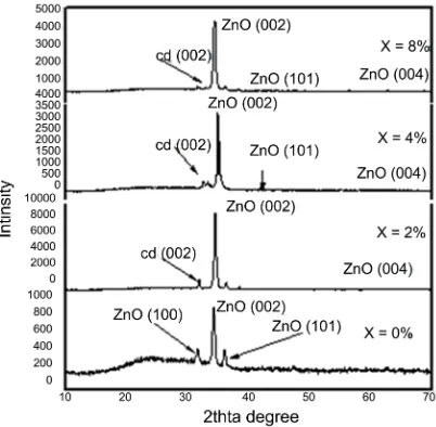
Figure 1 shows X-ray diffraction patterns of the as-prepared Zn100–xCdxO (x = 0,
2, 4, 6 and 8 at%) films. For the undoped ZnO film as seen in Figure 1(a) is po-lycrystalline with a hexagonal close-packed crystal lattice. The film has four prominent peaks of (002), (100), (101) and (004) plane with highly preferred orientation along the (002) direction as recorded in card No. 04-0831. As the concentration of CdO increases from x = 2 to 8 at% in the as-prepared Zn100–xCdxO thin films, the main peaks appear at 2θ = 31.635˚, 66.34˚, 36.15˚,
38.74˚, 43.029˚, and 77.076˚, which corresponded to Cd (002), (004) and Zn (002), (100), (101), (004) with highly preferred orientation along the (002) as seen in Figures 1(a)-(d). The intensity of the Cd (002) peak increases and be-comes more and more prominent at x = 4 at% as shown in Figures 1(b)-(d).
The X-ray diffraction patterns of annealed Zn100–xCdx (x = 0, 2, 4, and 8 at%)
thin films at 300˚C for 1h are shown in Figures 2(a)-(d) indicate that, it pos-sesses a polycrystalline hexagonal wurtzite structure with a preferred orientation along the ZnO2 (200) plane at 2θ = 36.96. For x = 0.0, the peaks appear at 2θ =
33.88˚, 35.02˚, 36.96˚, 39.71˚, 43.94˚ and 77.62˚, which correspond to Zn (002), (100), ZnO (200), Zn (100), ZnO2 (101) and (004) planes respectively as seen in Figure 2(a). Doping Cd with x = 2%, three peaks appear at 2θ = 35.02˚, 37.04˚ and 77.9˚ for Cd (100) and ZnO2 (200), (004) respectively as shown in Figure 2(b). For x = 4% the main peaks appear at 2θ = 33.46˚, 35.17˚, 37.11˚ and 77.9˚ which corresponding to Cd (002), CdO2 (200) and ZnO2 (200), (004) plane
re-spectively as clear in Figure 2(c). In additions, increasing x to 8 at%, the main peaks appear at 2θ = 32.44˚, 36.98˚, 39.06˚, 43.91˚ and 77.78˚, which corres-ponding to Cd (002), ZnO2 (200), (004) and Zn (100) Zn (101) planes
respec-tively as demonstrated in Figure 2(d). It is obvious that the crystal quality of the sample increases remarkably, and CdO (200) diffraction peak is observed, sug-gesting the phase segregation of CdO from the matrix phase [20]. Generally, this angular peak positions are greater than the as-prepare associated values. This trend can be ascribed to the tensile stresses that usually build in the furnace [21]. Also, the intensity ratio of ZnO and Cd peaks is decreased after annealing.
DOI: 10.4236/oalib.1104687 5 Open Access Library Journal
Figure 1. X-ray diffraction of as deposited Zn100−xCdxO thin films.
Figure 2. X-ray diffraction of Zn100−xCdxO thin films annealing at 300˚C for 1 h.
[image:5.595.244.501.419.642.2]DOI: 10.4236/oalib.1104687 6 Open Access Library Journal
Figure 3. X-ray diffraction of Zn100−xCdx thin films annealing at 500˚C for 1 h.
appear at 2θ = 31.50˚, 34.17˚, 35.95˚ corresponding to ZnO in the direction (100), (002) and (101) plane. For x = 2% Figure 3(b) the main peaks appear at 2θ = 31.75˚, 34.39˚ for Cd (002) and ZnO (002) respectively.
Doping Cd with x = 4% as seen in Figure 3(c) the main peaks appear at 2θ = 31.75˚, 34.39˚, 36.24˚, 38.32˚ and 72.56˚ which correspond to Cd (002), ZnO (200), ZnO (002), (101), (004) respectively. Finally, for x = 8% Figure 3(d) the main peaks appear at 2θ = 31.54˚, 32.92˚, 34.31˚, 36.04˚ and 72.46˚ relating to Cd (002), ZnO (002), (002), (101) and (004) respectively.
From above, it is clear that Zn and Cd only appeared in the X-ray diffraction of the as-prepared films, whereas, ZnO and CdO are shown after annealing at 300˚C for 1 h, besides, ZnO and Cd exists in the X-ray diffraction patterns with annealing temperature 500˚ results in
3.2. Optical Properties of the Thin Films
The typical UV-VIS-NIR optical transmittance and reflectance spectra of an-nealed films (Zn100−xCdx with x = 4 at%) at different annealing temperature as a
function of wavelength in the range from 300 to 2500 nm are shown in Figure 4
and Figure 5 respectively. It is clear that the transmittance increases and the ref-lectance decreases with increasing the annealing temperature from 200˚C to 450˚C. In Figure 4, the drop-off of the values of transmission belonging to the shorter wavelengths was related to the fundamental absorption by band-to-band transition. Meanwhile, the wavelength of the absorption edge decreased with an increase in temperature of annealing.
From the transmittance data it is possible to infer the optical energy gap of the films by plotting (αhυ)2 vs hυ (where α is the absorption coefficient, and hυ the
DOI: 10.4236/oalib.1104687 7 Open Access Library Journal
Figure 4. Spectral variation of the transmittance T% of annealed Zn100−xCdx (x = 4%) at
[image:7.595.272.473.295.469.2]different temperature.
Figure 5. Spectral variation of the reflectance R% of annealed Zn100−xCdx (x = 4%) at
dif-ferent temperature.
Figure 6. The variation of the Optical Band gap of the Zn100−xCdx (x = 4%) at different
[image:7.595.270.476.519.692.2]DOI: 10.4236/oalib.1104687 8 Open Access Library Journal
3.31 eV, which can be explained as follows: the unsaturated defects are gradually annealed out producing a larger number of saturated bonds leading to decreases in the density of localized states and consequently the optical gap increased [22].
The variations of refractive index and the extinction coefficient in the visible wavelength range of (Zn100−xCdx with x = 4 at%) films annealed at different
tem-perature are depicted in Figure 7. The refractive index of the films decreases with increasing the annealing temperature which can be attributed to the de-crease in the packing density with annealing temperature. On the other hand, the extinction coefficient (k) decreases with increasing the annealing tempera-ture, which can be attributed to the increase of the film transparency [23].
The packing density P of the film can be estimated from the following equa-tion [24]:
(
)
(
)
(
)
(
)
4 2
2
2 2
1 1
,
1 1
y y s
f
y s
p n p n n n
p n p n
− + +
=
+ + −
where nf is the refractive index of Zn100−xCdx with x = 4 at% films, ns is the
re-fractive index of the solid part of the film, that for single crystal ny Is the
refrac-tive index of the voids (equals one for air) and P is the packing density. It is ob-servable also that the extinction coefficient decreases with increasing the an-nealing temperature. This could be correlated to the decrease of absorption with increasing the temperature of annealing, where K = λα/4π is the absorption
coefficient [25].
3.3. Electrical of the Electrical Properties of the Thin Films
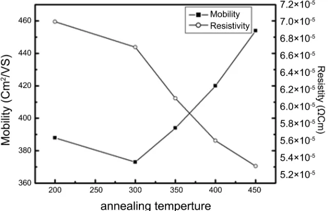
[image:8.595.218.538.480.686.2]The dependence of electrical properties on the temperature of annealing is shown in Figure 8. The resistivity decreases as the temperature is increased up
Figure 7. The variation of the mobility and resistivity of the Zn100−xCdx (x = 4%) at
DOI: 10.4236/oalib.1104687 9 Open Access Library Journal
[image:9.595.240.506.71.251.2]Figure 8. The variation of the of refractive index (n) and extinction coefficient (k) the Zn100−xCdx (x = 4%) at different annealing temperature.
Figure 9. The variation of the Factor of merit of the Zn100−xCdx (x = 4%) at different
an-nealing temperature.
to 450˚C showing semiconductor behavior. The lowest resistivity value 5.3 × 10 − 5 Ω-cm has been obtained for annealed film at temperature of 450˚C. It is ob-servable also that, the carriers mobility increased with increase in annealing temperature. This may be due to the increase of the grain size with increase in annealing temperature, and this leads to reduction of the grain boundary scat-tering due to charge carriers. The decrease of the electrical resistivity of annealed films is due the increase of the mobility carriers.
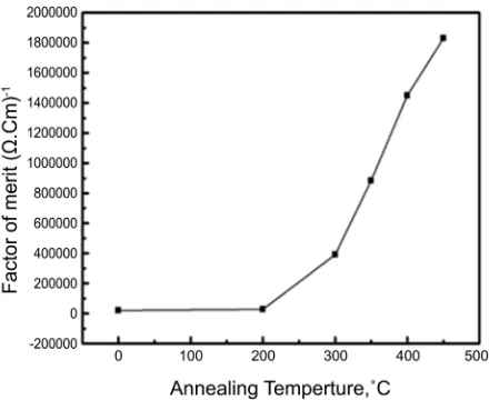
In order to predict the selective properties of transparent conductive coatings from the fundamental optical and electrical properties, the factor of merit can be employed ϕ=Tm ρ [26] where Tm is the average transmittance in the visible
region and ρ is the electrical resistivity. Figure 9 shows the variation of the
[image:9.595.265.485.297.477.2]DOI: 10.4236/oalib.1104687 10 Open Access Library Journal
4. Conclusion
Thin films of Zn100–xCdxO with x = 0, 2, 4, 6 and 8 at% have been deposited by
electron beam evaporation technique. The effect of heat treatment on the elec-trical, optical and structural properties of these films was carried out. For con-tent of cadmium oxide at 4%, optical measurements indicated that, the optical energy gap, the mobility of the carriers, and the figure of merit increase with in-creasing the annealing temperature. On the other hand, our results indicate that, the refractive index, extinction coefficient, and the resistivity decrease with in-creasing the annealing temperature. The best value of the figure of merit found to be at annealing temperature 450˚C.
Conflicts of Interest
The authors declare no conflicts of interest regarding the publication of this pa-per.
References
[1] Sapoval, B. and Hermann, C. (1995) Physics of Semiconductors. Springer, New York. https://doi.org/10.1007/978-1-4612-4168-3
[2] Tiller, W.A. (1991) The Science of Crystallization. Vol. 1, Cambridge University Press, Cambridge.
[3] Shaw, B.J. (1967) Room Temperature Mechanical Properties of Cadmium-Zinc La-mellar Eutectic Alloys. Acta Metallurgica, 15, 1169-1177.
https://doi.org/10.1016/0001-6160(67)90391-4
[4] Sahoo, M., Porter, R.A. and Smith, R.W. (1976) Mechanical Behaviour of the Cd-Zn Eutectic Composite. Journal of Materials Science, 1, 1680-1690.
https://doi.org/10.1007/BF00737524
[5] Sahoo, M. and Smith, R.W. (1978) Mechanical Properties Characterization of the Pb-Cd Eutectic Composite. Journal of Materials Science, 13, 283-290.
https://doi.org/10.1007/BF00647771
[6] Cantor, B. and Chadwick, G.A. (1976) Thermal Stability of Eutectic and Off-Eutectic Ag-Cu, Cd-Zn and Al-ζ(AlAg) Alloys. Journal of Crystal Growth, 36, 232-238. https://doi.org/10.1016/0022-0248(76)90282-7
[7] Van de Merwe, R.H., Smith, R.W., Lemkey, F.D., Cline, H.E. and Mc Lean, M. (Eds.) (1982) In Situ Composites IV. Elsevie Science Publishing, Co., Amsterdam, p. 291.
[8] Kaya, M. and Smith, R.W. (1989) The Discontinuous Coarsening Reactions in the Pb Cd and the Zn Cd Lamellar Eutectic Alloys-I. The Driving Force, Initiation and the Morphology. Metall., 37, 1657. https://doi.org/10.1016/0001-6160(89)90132-6 [9] Jayakrishnan, R. and Hodes, G. (2003) Non-Aqueous Electrodeposition of ZnO and
CdO Films. Thin Solid Films, 440, 19-25.
https://doi.org/10.1016/S0040-6090(03)00811-3
DOI: 10.4236/oalib.1104687 11 Open Access Library Journal by Reactive Magnetron Sputtering and Subsequent Annealing. Journal of Vacuum Science & Technology A, 5, 1952. https://doi.org/10.1116/1.574889
[12] Sagar, P., Kumar, M. and Mehra, R.M. (2005) Influence of Hydrogen Incorporation in Sol-Gel Derived Aluminum Doped ZnO Thin Films. Thin Solid Films, 489, 94-98. https://doi.org/10.1016/j.tsf.2005.05.009
[13] Vigil, O., Cruz, F., Santana, G., Vaillant, L., Morales-Acevedo, A., Choi, Y.S., Lee, C.G. and Cho, S.M. (1996) Transparent Conducting ZnxCd1−xO Thin Films
Pre-pared by the Sol-Gel Process. Thin Solid Films, 298, 153.
https://doi.org/10.1016/S0040-6090(96)08923-7
[14] Ilican, S., Caglar, Y., Caglar, M., Kundakci, M. and Ates, A. (2009) Photovoltaic So-lar Cell Properties of CdxZn1−xO Films Prepared by Sol-Gel Method. International
Journal of Hydrogen Energy, 34, 5201-5207. https://doi.org/10.1016/j.ijhydene.2008.10.022
[15] Sui, Y.R., Yue, Y.G., Cao, Y., Yao, B., Liu, X.Y., Lang, J.H., Gao, M., Li, X.F., Li, X.Y. and Yang, J.H. (2014) Influence of Substrate Temperature on Structural and Optical Properties of ZnCdO Thin Films Deposited by DC Magnetron Sputtering. Ceramics International, 40, 9189. https://doi.org/10.1016/j.ceramint.2014.01.136
[16] Sui, Y., Yue, Y., Song, Y., Cao, Y., Yao, B., Lang, J., Li, X. and Yang, J. (2015) Effects of Cd Concentration on Microstructure and Optical Properties of the Ternary Zn1-xCdxO Alloy Thin Films Synthesized by Magnetron Sputtering. Materials Re-search Bulletin, 70, 348-353. https://doi.org/10.1016/j.materresbull.2015.05.004 [17] Bharath, S.P., Bangera, K.V. and Shivakumar, G.K. (2017) Properties of CdxZn1−xO
Thin Films and Their Enhanced Gas Sensing Performance. Journal of Alloys and Compounds, 720, 39. https://doi.org/10.1016/j.jallcom.2017.05.240
[18] Bera, A., Thapa, R., Chattopadhyay, K.K. and Saha, B. (2015) In Plane Conducting Channel at the Interface of CdO-ZnO Isotype Thin Film Heterostructure. Journal of Alloys and Compounds, 632, 343-347. https://doi.org/10.1016/j.jallcom.2015.01.168 [19] Ali, H.M. (2005) Characterization of a New Transparent-Conducting Material of
ZnO Doped ITO Thin Films. Physica Status Solidi A, 202, 2742-2752. https://doi.org/10.1002/pssa.200521045
[20] Ma, D.W., Ye, Z.Z., Huang, J.Y., Zhu, L.P., Zhao, B.H. and He, J.H. (2004) Effect of Post-Annealing Treatments on the Properties of Zn1−xCdxO Films on Glass
Sub-strates. Materials Science and Engineering B, 111, 9-13. https://doi.org/10.1016/j.mseb.2003.12.007
[21] Gupta, V. and Mansingh, J. (1996) Influence of Postdeposition Annealing on the Structural and Optical Properties of Sputtered Zinc Oxide Film. Applied Physics, 80, 1063. https://doi.org/10.1063/1.362842
[22] Ali, H.M., Abd-Raheem, M.M., Megahed, N.M. and Mohamed, H.A. (2006) Opti-mization of the Optical and Electrical Properties of Electron Beam Evaporated Aluminum-Doped Zinc Oxide Films for Opto-Electronic Applications. Journal of Physics and Chemistry of Solids, 67, 1823-1829.
https://doi.org/10.1016/j.jpcs.2006.04.005
[23] Mohamed, H.A., Ali, H.M., Mohamed, S.H. and Abd El-Raheem, M.M. (2006) Transparent Conducting ZnO-CdO Thin Films Deposited by e-Beam Evaporation Technique. The European Physical Journal Applied Physics, 34, 7-12.
https://doi.org/10.1051/epjap:2006039
[24] Maclend, H.A. (1986) Structure-Related Optical Properties of Thin Films. Journal of Vacuum Science & Technology A, 4, 418. https://doi.org/10.1116/1.573894
DOI: 10.4236/oalib.1104687 12 Open Access Library Journal Constants of Zn1−xLixO Films Prepared by Chemical Bath Deposition Technique.
Physica B, 366, 44. https://doi.org/10.1016/j.physb.2005.05.019
[26] Ali, H.M., Mohamed, H.A. and Mohamed, S.H. (2005) Enhancement of the Optical and Electrical Properties of ITO Thin Films Deposited by Electron Beam Evapora-tion Technique. The European Physical Journal Applied Physics, 31, 87.