Reverse Current Conduction Mechanism of Transient Voltage Suppression Diode
under Electrostatic Discharge Stress
Daoheung Bouangeune
1, Ye-Ji Lee
1, Deok-Ho Cho
2, Kyu-Hwan Shim
1,2,+and Chel-Jong Choi
1,+1School of Semiconductor and Chemical Engineering, Semiconductor Physics Research Center,
Chonbuk National University, Jeonju 561-756, Republic of Korea 2R&D Division, Sigetronics, Inc., Jeonju 561-756, Republic of Korea
A transient voltage suppression (TVS) diode with abrupt junctions was fabricated using low-temperature epitaxy. The effect of electrostatic discharge (ESD) stress on the reverse leakage current conductive mechanism of the TVS diode was investigated using IEC61000-4-2 (IEC) standard analysis, in accordance with temperature-dependent current-voltage (I-V) characteristics. The fabricated TVS diode showed excellent ESD robustness, with negligible degradation up to«19.5 kV and failure at«20 kV stress. The ESD stress evidently led to the generation of shallow and deep defect states in the depletion region located 0.521.08 eV below the conduction band, and these states served as a main contributor to the resulting reverse leakage current. In devices to which IEC peak voltage stresses of less than«19.5 kV had been applied, reverse conduction was dominated by generation-recombination current; the application of the«20 kV failure stress caused reverse conduction to become dominated by a combination of tunneling current via deep defects and Poole-Frenkel barrier lowering. The proposed TVS can serve as a highly stable and reliable ESD protector of electronic components, serving an evolving need in nanoscale technology.
[doi:10.2320/matertrans.M2014214]
(Received June 11, 2014; Accepted August 4, 2014; Published October 3, 2014)
Keywords: transient voltage suppression (TVS) diode, electrostatic discharge (ESD), TVS, IEC61000-4-2, carrier transport mechanism, activation energy
1. Introduction
The scaling down of device size to realize low-voltage operation in integrated circuits (ICs) has led to an increase in the probability of damage by electrostatic discharge (ESD).1,2) Today, ESD has adverse effects on productivity
and reliability in virtually every aspect of electronic components and systems.3)Thus, the development of highly
stable and reliable ESD protective devices such as transient voltage suppression (TVS) diodes, offering low leakage current and clamping voltage as well as immunity to ESD snapback, is essential to the IC industry.47)Typically, a TVS diode is assembled with elements or circuits that provide protection in the reverse direction, and operates under reverse bias conditions. The reverse leakage current and ESD strength are considered to be important parameters for evaluating the performance of TVS diodes. An ideal TVS diode should be non-conductive under normal operating voltage, but should respond to a transient voltage pulse greater than the TVS’breakdown voltage, such as an ESD event, by undergoing avalanche breakdown and passing excess transient current from the protected input/output line to ground. Although TVS diodes have been widely used to protect electronic components from ESD damage, they are themselves susceptible to performance degradation or failure under very large ESD shocks that are sufficiently strong to damage their p-n junction layers.7) Typically, such damage introduces a defect state in the bulk device, which can become a main source of leakage current.8,9)This can lead to jitter noise in digital and analog circuits, leading to poor reliability in the long term.10,11)Despite this problem, there have been few reports on the effects of such large ESD events upon the carrier conduction mechanism of the TVS diode in the reverse bias regime. Herein we describe the fabrication
of a TVS diode with abrupt multi-junctions using a low-temperature epitaxy process, and discuss its ESD perform-ance. In particular, current-voltage (I-V) characteristics were measured at various temperatures to investigate the effect of ESD stress on the reverse leakage current conductive mechanism of a TVS diode.
2. Experimental Details
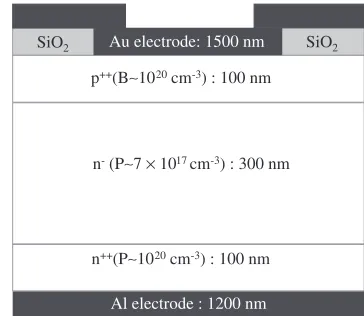
Figure 1 shows a schematic diagram of the TVS diode fabricated in this work. To fabricate the diode,first, a heavily doped n-type Si (100) wafer was cleaned in HF solution to remove impurities and native oxide. To form the abrupt multi-junctions, n- and p-type epitaxial Si layers were then sequentially grownin situby the addition of diborane (B2H6)
and phosphine (PH3) gases, respectively, using a
reduced-pressure chemical vapor deposition (RPCVD) system. The RPCVD process was performed at the low temperatures of 600800°C to minimize the degradation of device
perform-n++(P∼1020cm-3) : 100 nm SiO2 SiO2
n-(P∼7 × 1017cm-3) : 300 nm p++(B∼1020cm-3) : 100 nm
Au electrode: 1500 nm
Al electrode : 1200 nm
Fig. 1 Schematic cross-sectional view of the proposed TVS diode.
+Corresponding author, E-mail: khshim@jbnu.ac.kr, cjchoi@jbnu.ac.kr
[image:1.595.333.515.357.515.2]ance caused by the use of higher temperatures; conventional high-temperature drive-in processes tend to form linearly graded junctions that are associated with concentrations of non-uniform local electric fields in the SiO2/Si interfaces.
To form the top electrode, a 1500 nm-thick Au film was
deposited by means of an e-beam evaporator, followed by patterning with a 140©140-µm2square shape using lift-off lithography. Finally, a 1200 nm-thick Al film was formed on the backside of the wafer, to serve as a back electrode. Temperature-dependent current-voltage (I-V-T) measure-ments were performed using a semiconductor parameter analyzer (Agilent 4155A) equipped with a probe station. The temperature was controlled using a thermal chuck attached inside a shielded cover. The effects of ESD events were analyzed using an ESD simulator ESS-2000 with a discharge gun TC-815R, following the IEC61000-4-2 standard. The TVS diode was subjected to 10 discharges of both positive and negative polarities, at 1 s intervals.
[image:2.595.318.534.68.236.2]3. Results and Discussion
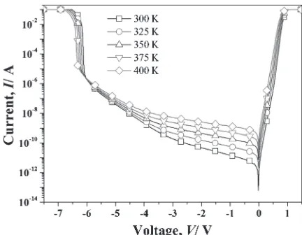
Figure 2 shows I-V-T measurements of an as-fabricated TVS diode over the wide temperature range of 300400 K. These diodes were rated to 4.8 V, with avalanche breakdown at 6 V; they were fabricated to meet this rating by controlling the doping concentration and epi-layer thickness of the base layer. Generally, fabricating a diode with low breakdown voltage is carried out by using a narrow, lightly doped layer, but this dramatically increases the reverse leakage current, leading to poor reliability and noise performance in the system. Contrastingly, in this work, the use of an abrupt and uniform junction yielded room-temperature reverse leakage current of less than 10¹7A at the reverse bias of¹4.8 V. The
positive temperature coefficient (PTC) of the breakdown voltage (¦BV) was measured to be 1 mV/K at 10¹6A, confirming that the carriers were Boltzmann distributed, as is typical in most semiconductor materials, and also confirming that avalanche breakdown was the typical mode of break-down in these devices. A lower reverse leakage current is essential to ensure improvements in the reliability and ESD performance of TVS diodes.7)
A comparison of room-temperature I-V characteristics of a TVS diode taken before and after it experienced various IEC stresses demonstrates the TVS device’s excellent strength against IEC stress, as shown in Fig. 3. Namely, its I-V behaviors were unchanged with increasing IEC stress up to
«19.5 kV. However, the«20 kV IEC stress produced a rapid increase in the reverse leakage current, which is a typical signature of electrical failure. Scanning electron microscope
(SEM) analysis revealed that «20 kV IEC stress caused
pinholes to form on the surface of the Au electrode, surrounded by refrozen features, indicating that severe damage of the epitaxially grown multi-junction at this stress level could be a main cause of device failure (the inset of Fig. 3).
The ESD tests described above demonstrated that ESD stress induced increased leakage current, and it is apparent that the ESD stress affected the mechanism of carrier transport through the p-n junction. Therefore, to understand the junction structures’failure mechanism, the effects of ESD
stress on the reverse current conduction mechanism need to be studied. Because the p-n junction is the core structure of a TVS diode, the reverse leakage current conductive mechan-ism for p-n junctions is valid for analysis of TVS diodes. Actually, analyzing the temperature dependence of the reverse current has proved to be useful in investigating the reverse leakage current conduction mechanism.1214)For the
one-sided abrupt junction, the reverse current given by the Shockley equation can be expressed as15)
Irev ¼Sq ffiffiffiffiffiffiffi Dp
¸p s
n2i NDþ
eSWni
¸g ð1Þ
where S is the p-n junction area, ND is the base doping
concentration,Wis the depletion region width,Dpis the hole
diffusion coefficient, ¸p is the mean hole recombination
lifetime and ¸g is the mean time to generate electron-hole
pairs. Because ni³exp(¹Eg/2kBT), the temperature
de-pendence of the exponential terms is stronger than that of the other term; thus, eq. (1) can be rewritten as
Irevexp Eg kBT
þexp Eg
2kBT
ð2Þ
Fig. 2 I-V characteristics of the as-fabricated TVS diode, measured at various temperatures ranging from 300 to 400 K.
[image:2.595.312.540.278.454.2]The activation energy (Ea) is defined as the slope of lnIRev
versus 1/kBT. In principle,Eashould be close to the Si band
gapEgorEg/2 in the diffusion- or
generation-recombination-dominated regimes, respectively. It is well known that carriers generated inside the depletion region are the main constituent of the generation current, and that the generation current dominates at low temperature. Contrastingly, the diffusion current is caused by the diffusion of minority carriers approaching the depletion edge, and dominates at high temperature. In this study, we analyzed the reverse leakage current conduction mechanism at a reverse bias of less than ¹3 V, while varying the temperature from 300 to 350 K, in order to avoid junction breakdown or tunneling due to high electric field and thermal treatment defects. The temperature-dependent I-V curves were measured initially, and again following each application of ESD stress.
Figure 4 represent the plot of Ea (as calculated from the
slope of lnIR¹1/kBTplot in the inset of Fig. 4) as a function
of the base doping concentrations ranging from 1©1017 to 7©1017cm¹3. It is clear that an increase in the base doping concentration led to a gradual decrease in Ea. This strongly
indicated that the increase in base doping density induced deeper defect states in the depletion region of junction located below the conduction band. Generally, typical defect states can play a role of recombination centers, which are the mainly contributors for the reverse leakage current. Fur-thermore, for TVS diode with base doping concentrations in the range of 1©1017³5©1017cm¹3, the values of E
a
were close toEg/2. This implies that
generation-recombina-tion was their dominant carrier conducgeneration-recombina-tion mechanism in reverse bias regions. However, as for TVS diode having the base doping concentration of 7©1017cm¹3, theEawas less
than Eg/2, indicating that its reverse leakage current was
dominated by both generation-recombination and other
field-enhancement processes.16)
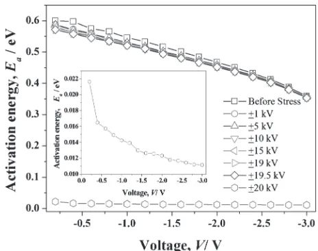
Figure 5 exhibits the plot ofEaversus reverse bias ranging
from¹0.2 V to¹3 V after the application of various levels of IEC peak voltage stress. TheEawas calculated from the slope
of lnIrevvs. 1/kBTplot (Fig. 6) for the proposed TVS diode
with ND=7©1017cm¹3before and after the application of
IEC stress, at various reverse biases in the temperature range of 300350 K. Notably, with increasing IEC peak voltage stress up to «19.5 kV, the activation energy of the leakage current as measured at the reverse bias of ¹0.2 V slightly decreased from 0.6 to 0.56 eV and it suddenly decreased to 0.02 eV by«20 kV stress. The ESD stress evidently induced defect states in the junction depletion region located 0.50 1.08 eV below the conduction band (at the reverse bias of
¹0.2 V), which could be a main cause of the reverse leakage current. As shown in Fig. 5,Eawas close toEg/2 except in
the device subjected to «20 kV stress, and decreased with increasing reverse voltage. It is evident that, for IEC peak
voltage less than «19.5 kV stress, the reverse leakage
currents cannot be accounted for by the thermal generation-recombination current alone. But they are thought to be impacted by the Poole-Frenkel lowering effect when IRwas
exponential dependence on the applied voltage as shown in
Fig. 4 Plot ofEaas a function of the base doping concentrations of TVS
diodes. Inset shows the Arrhenius plot of the reverse leakage current for the TVS diodes with base doping concentration ranging from 9©1016to
7©1017cm¹3at various reverse biases of 2 V.
Fig. 5 Plot ofEaextracted from the TVS diode withND=7©1017cm¹3
versus reverse bias at various levels of IEC peak voltage shock ranging from 0 to «20 kV. Reverse bias dependency of Ea for TVS diode
subjected to«20 kV stress is shown enlarged in the inset.
Fig. 6 Arrhenius plot of the reverse leakage current for the proposed TVS diode withND=7©1017cm¹3before and after the application of IEC
[image:3.595.55.282.67.250.2] [image:3.595.310.542.68.251.2] [image:3.595.312.539.323.506.2]Fig. 2 and Fig. 3. The Poole-Frenkel barrier lowering effect is known as a Coulombic potential barrier lowering due to the external application of an electric field.17) When dominated by the Poole-Frenkel barrier lowering effect, the reverse leakage current can be given as13)
IR/Eexp q kT
ffiffiffiffiffiffiffi qE ³¾
r !
ð3Þ
Slope¼ q
kT ffiffiffiffiffiffi
q ³¾ r
ð4Þ
where ¾ and E are the permittivity of Si and the maximum electric field in the junction, respectively. For an applied voltageVA,Eis estimated asE¼ ðVbiVAÞ=dCV, whereVbi
is the built-in voltage of the TVS diode and dCV is the
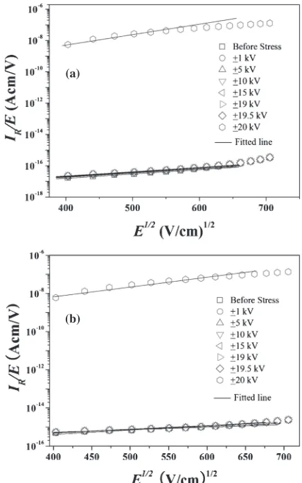
depletion width; these were obtained from theC-V character-istic curve (data not shown). The slopes calculated for the Poole-Frenkel barrier lowering effect using eq. (4) were 0.00853 and 0.0073 (V·cm)1/2at 300 and 350 K, respectively. Table 1 summarizes the experimental slope for the Poole-Frenkel barrier lowering effect, as evaluated from a plot of IR/E versus E1/2 (Fig. 7). Notably, the experimental slopes
were close to the calculated values for both 300 and 350 K, indicating that the reverse leakage currents for a TVS diode subjected to various level IEC peak voltages less than
«19.5 kV were dominated by the Poole-Frenkel barrier
lowering effect and the thermal generation-recombination mechanism.
For the device subjected to the failure stress of«20 kV,Ea
dropped suddenly from 0.57 to 0.02 eV (Fig. 5) and showed dependency on bias voltage (inset of Fig. 5). This could be attributed to the thermal excitation of the electrons through deep defect states located 1.08 eV below the conduction band to the conduction band in the depletion region known as trap-assisted carrier tunneling.18) Moreover, the Poole-Frenkel effect is also involved since the experimental slopes are close to the calculated value for both 300 and 350 K (see Table 1). In addition, the«20 kV stress caused the metalfilm contact and p-n junction to burn (inset of Fig. 3). Meanwhile, the Au electrodefilm could conceivably be spiked through the p++ layer to the n¹ layer, thereby forming a Schottky contact; however, this appears not to be the case. The formation of such a Schottky contact would have an effect on the reverse
leakage current conduction mechanism. When dominated by the Schottky barrier lowering effect, the reverse leakage current can be given as13)
IR/T2exp 2q kT
ffiffiffiffiffiffiffi qE ³¾
r !
ð5Þ
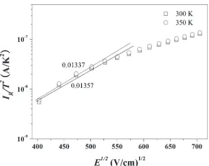
The calculated slopes for Schottky barrier lowering equal half the result of eq. (4); that is, 0.0042 and 0.0036 (V·cm)1/2at 300 and 350 K, respectively. However, the experimental slopes for the Schottky barrier as evaluated from a plot of IR/T2 versus E1/2 (Fig. 8), were much larger than these
calculated values. This indicated that the reverse leakage current was not impacted by the Schottky barrier lowering effect; rather, the trap-assisted carrier tunneling mechanism and the Poole-Frenkel barrier lowering effect dominated in this case.
4. Conclusion
The fabricated TVS diode showed excellent ESD strength, functioning after the application of up to «19.5 kV of IEC peak voltage and failing upon the application of «20 kV stress. The ESD stress induced both shallow and deep defect
states in the depletion region 0.521.08 eV below the
conduction band (at reverse bias of¹0.2 V). In as-fabricated devices and those to which sub-failure voltage stress were
Table 1 Summary of the calculated and experimental slopes for the Poole-Frenkel barrier lowering effect at 300 and 350 K.
IEC Peak voltage/kV
300 K 350 K
Calculated/ (V·cm)1/2
Experimental/ (V·cm)1/2
Calculated/ (V·cm)1/2
Experimental/ (V·cm)1/2
0
0.0085
0.0085
0.0073
0.0064
«1 0.0081 0.0062
«5 0.0078 0.0060
«10 0.0078 0.0059
«15 0.0075 0.0060
«19 0.0078 0.0060
«19.5 0.0077 0.0061
«20 0.0082 0.0094
(a)
(b)
Fig. 7 Plot of IR/E versus E1/2 for the Poole-Frenkel barrier lowering
[image:4.595.46.291.93.231.2]applied, carrier conduction in the reverse bias regions was dominated by generation-recombination current. On the other hand, upon application of the failure stress, the devices’ reverse conduction mechanism became dominated by both tunneling current via deep defects and the Poole-Frenkel barrier lowering effect. These results indicate that ESD pulses below the critical value did not affect the reverse leakage current conduction mechanism of the TVS diode. Thus, the proposed TVS diode can serve as a highly reliable device to protect sensitive electronic components from ESD damage.
Acknowledgements
This research was supported by Basic Research Labo-ratory Program (2011-0027956) through the National Re-search Foundation of Korea funded by the Ministry of Education, Science and Technology, Republic of Korea,
and by the Converging Research Center Program
(2014M3C1A8048834) through the Ministry of Science, ICT & Future Planning, Republic of Korea. It was also was supported by a grant from the R&D Program for Industrial Core Technology funded by the Ministry of Trade, Industry and Energy (MOTIE), Republic of Korea (Grant No. 10045216).
REFERENCES
1) A. Z. Wang, H. G. Feng, K. Gong, R. Y. Zhan and J. Stine:
Microelectron. J.32(2001) 733747.
2) A. Amerasekera and C. Duvvury:IEEE Trans. Compon. Pack. Manuf. Technol.18(1995) 314320.
3) R. Merri and E. Issaq: Proc. EOS/ESD Symp.15(1993) pp. 233237. 4) D. Bouangeune, W.-K. Hong, S. S. Choi, C. J. Choi, D. H. Cho, J. M. Park, J. H. Lee, H.-D. Yang and K. H. Shim: Proc. 1st IEEE GCCE, Tokyo, Japan, (2012) pp. 189192.
5) S. S. Choi, D. H. Cho and K. H. Shim:Electron. Mater. Lett.5(2009) 5962.
6) T. Green: Proc. EOS/ESD Symp. (1988) pp. 714.
7) D. Bouangeune, Y.-H. Kil, S.-S. Choi, D.-H. Cho, K.-H. Shim and C.-J. Choi:Mater. Trans.54(2013) 21252130.
8) M. Diatta, D. Trémouilles, E. Bouyssou, R. Perdreau, C. Anceau and M. Bafleur:IEEE Trans. Electron Devices59(2012) 108113.
9) J. Cambieri, W. Reinprecht, F. Roger, A. Wagner and R. Minixhofer: Proc. 34th EOS/ESD Symp. (2012) pp. 16.
10) F. Hou, G. Bosman, E. Simoen, J. Vanhellemont and C. Claeys:IEEE Trans. Electron Devices45(1998) 25282536.
11) I. Wey, Y.-G. Chen, Ch.-H. Yu, A.-Y. A. Wu and J. Chen:IEEE Trans. Circuits Syst. I-Regul. Pap.56(2009) 24112424.
12) V. V. N. Obreja and A. C. Obreja:Phys. Status Solidi A207(2010) 12521256.
13) H.-D. Lee, S.-G. Lee, S.-H. Lee, Y.-J. Lee and J.-M. Hwang:Jpn. J. Appl. Phys.37(1998) 11791183.
14) A. Czerwinski, E. Simoen, A. Poyai and C. Claeys:J. Appl. Phys.94
(2003) 12181221.
15) S. M. Sze and K. K. Ng:Physics of Semiconductor Devices, (Wiley, New Jeresy, 2007).
16) H. D. Lee:IEEE Trans. Electron Devices47(2000) 762767.
17) J. Frenkel:Phys. Rev.54(1938) 647648.
18) Q. Shan, D. S. Meyaard, Q. Dai, J. Cho, E. F. Schubert, J. K. Son and C. Sone:Appl. Phys. Lett.99(2011) 253506.
Fig. 8 Plot of IR/T2 versus E1/2 for Schottky barrier lowering under
[image:5.595.63.277.67.237.2]