Khyoupin Khoo
1;*, Jin Onuki
1, Takahiro Nagano
1, Suguru Tashiro
1, Yasunori Chonan
2,
Haruo Akahoshi
3, Toshio Haba
3, Toshimi Tobita
4, Masahiro Chiba
4and Kensuke Ishikawa
51
Department of materials science and Engineering, Ibaraki University, Hitachi 316-8511, Japan
2Department of Electronics and Information System, Faculty of System Science and Technology,
Akita Prefectural University, Honjyo 015-0055, Japan
3Hitachi Research Laboratory, Hitachi Ltd., Hitachi 319-1292, Japan 4Hitachi Kyowa Engineering Ltd., Hitachi 319-1292, Japan
5Micro Device Division, Hitachi Ltd., Tokyo 198-8512, Japan
Grain size distributions and average grain sizes in the longitudinal direction of the Cu interconnect in 50-, 70- and 80-nm-wide Cu interconnects were evaluated and compared with the resistivities of each interconnect. After annealing, the standard deviation of grain sizes for 50-nm Cu interconnect increased to 27.5, and the average grain size microstructure grew to larger than that of as-deposited 50-nm Cu interconnects. The value of standard deviation of grain sizes in the normal distribution histogram for a 50-nm wire was found to be much smaller than those for 70- and 80-nm Cu wires after annealing. This implies that adequate grain growth should not be expected in the very narrow Cu interconnects (less than 50-nm) of the future if they are made with the conventional annealing process.
[doi:10.2320/matertrans.MRA2007611]
(Received April 23, 2007; Accepted July 12, 2007; Published August 29, 2007)
Keywords: copper interconnects, longitudinal microstructure, ultralarge-scale integration circuits, resistivity, mean free path
1. Introduction
In recent years, the continuous progress in fabrication of high performance ultralarge-scale integration circuits (UL-SIs) has been driven by the desire to increase circuit speed, broaden chip functionality, and improve reliability of electronic interconnects. In response to these technical demands, a high integration LSI using the 65-nm technology node (90-nm line width) has already been commercialized, and Cu interconnects for a 45-nm technology node (70-nm line width) LSI are under development, and will be in use by the 2010, according to the International Technology Road-map for Semiconductors (ITRS).1)
However, there is a significant increase in resistivity in copper interconnects when line widths are less than 100 nm.1–7) This is becoming a critical issue and is mainly due to the fact that the line widths are comparable to the mean free path of an electron (39 nm), which causes an increase in resistivity by electron scattering occurring at the grain boundaries of the Cu interconnects. Therefore, it is necessary to develop a grain coarsening process to achieve low resistivity in very narrow Cu interconnects.
Researchers have recently investigated cross-sectional microstructures and the resistivity of Cu films and inter-connects8–12) and reported experimental results for the microstructure have,e.g., an investigation of the grain sizes from the surface plane of Cu interconnects using an orientation imaging microscope (OIM)8) or TEM (plane-view measurement).10) However, this investigation did not clarify the longitudinal grain size distribution that control resistivity.
Microstructures in the longitudinal direction of Cu interconnects with line widths greater than 170 nm that use electron backscattered diffraction (EBSD) have also been
investigated.13)But there have been no reports on grain size distribution in the longitudinal direction of Cu interconnects of less than 100 nm. This is because the fabrication of Cu interconnects of less than 100 nm in the longitudinal direction is very difficult. We have succeeded in fabricating 80-nm-wide Cu interconnects along the longitudinal direction using focused ion beam (FIB) milling. Observations using field emission transmission electron microscopy (FETEM) tech-niques revealed that larger grains are predominant in the top part, and smaller grains are predominant in the bottom part of Cu trenches.14,15)
We assume sidewall-restricted grain growth at the bottom of narrow trenches, resulting in grain size distributions in the depth direction of the trench. The grain growth processes of a Cu interconnect strongly depend on trench widths, so the resistivity of next generation Cu interconnects using the 32-nm technology node (50-32-nm line width) is expected to increase further.
In this study, we statistically investigated the longitudinal grain size distributions of 50-nm-wide Cu interconnects and compared them with those of 70- and 80-nm-wide Cu interconnects. The resistivity of 50-nm wires was then compared with those of the 70- and 80-nm-wide Cu wires. After presenting our findings, we will discuss the possibility creating low resistivity Cu interconnects narrower than 50 nm.
2. Experimental Procedure
order. The thickness of the TaN/Ta barrier layer was estimated from the TEM images and was reduced to 5– 8 nm (nominal 15 nm) due to sidewall shadowing during deposition in the Cu trenches.
The Cu interconnects in this study were made by the DC electroplating process using a pure copper electrolyte at room temperature with a current density of 5 mA/cm2. The bath
compositions were composed of commercial CuSO45H2O,
HCl and H2SO4 solution with additives. After DC
electro-plating, the resulting fine-grained Cu film deposition was found to be under a high degree of intrinsic stress due to an excess of vacancies and dislocations.16) This condition is unstable and this strain energy can only be remedied by recrystallisation. Thus, to expedite recrystallization of the electroplated copper, these substrates were annealed at 400C
for 0.5 h in pure H2ambient and then subjected to chemical
mechanical polishing (CMP) to remove excess Cu film from the trenches. The substrate-annealed pre-CMP had an over-burden of Cu film with a thickness of 300 nm,i.e., the line height of the Cu trenches.
The as-deposited Cu interconnects had a smaller grain size and a higher resistivity than those that were annealed. Thus, coarsening the grain size in the narrow Cu interconnects is very important to reducing the resistivity. After annealing, the grains are larger and the grain boundary scattering is smaller, reducing the resistivity of the Cu interconnects. However, the coarsening of the Cu grains may be restricted by the sidewalls of very narrow trenches.15)
To clarify the grain sizes and their distributions inside the Cu interconnects with line widths of 50 nm, we investigated the cross-sectional microstructures in the longitudinal direc-tion of the Cu wires using a focused ion beam (FIB) instrument (Hitachi FB-2000A).14)Before FIB milling, 100-nm-thick carbon films were evaporated onto the samples to protect the Cu wires from damage during milling. Gaþ ion
beams accelerated at 30 kV were rastered along the Cu wires to cut holes on both sides precisely at the object portion. The resulting freestanding Cu films were placed into a field emission transmission electron microscope (FETEM) to observe the longitudinal microstructures. The observed Cu interconnect wires were about 4-mmlong with a thickness of approximately4050nm.
3. Experimental Results and Discussion
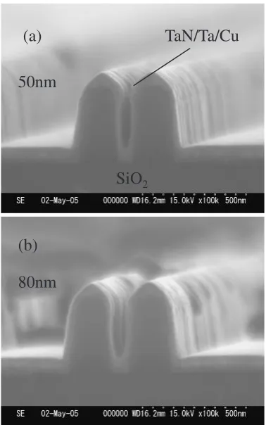
Figure 2(a) and (b) show cross-sectional SEM images of Cu electroplated trenches of 50- and 80-nm widths after annealing, as revealed by FIB milling. Representative SEM images show that the 50- and 80-nm-wide trenches with line heights of 300 nm were completely filled with electroplated copper. Figure 2(c) and (d) show a surface view SEM image of 50- and 80-nm-wide Cu interconnects after CMP. It can be seen that the wires were not dished or eroded during the CMP.
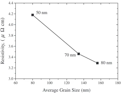
Figure 3 shows the resistivity of Cu interconnects with heights of 300 nm after annealing at 400C for 0.5 h. The
resistivity of the Cu interconnects increases significantly as line widths decrease to less than 100 nm,i.e., the average value is 3.23m-cm for an 80-nm width, 3.48m-cm for a 70-nm width, and reaches an average value of about 4.18m -cm for a 50-nm-width.
50nm
80nm
(a)
(b)
TaN/Ta/Cu
SiO
2Fig. 1 SEM images of as-etched 50-nm and 80-nm-wide damascene trenches after ultrathin TaN/Ta (TaN: 7.5 nm; Ta: 7.5 nm) barriers and a 55-nm-thick Cu seed layer were sputter-deposited into trenches prior to electroplating.
[image:2.595.311.541.70.313.2] [image:2.595.74.263.71.373.2]Two methods were used to quantify grain sizes and grain size distributions of the 50-nm-wide Cu interconnects in the longitudinal direction in comparison with those of 70- and 80-nm-wide interconnects, as shown in Fig. 4. For grain length distribution in the trench depth direction, straight horizontal lines were drawn from the bottom to the surface of the trenches in 10-nm steps, and the length of intercepts between the horizontal lines and each grain at the depth of the trenches was obtained and averaged. This grain length exhibits grain size distribution in the depth direction. To obtain grain sizes, a line was drawn around the grain boundary of each grain in the trench, the sizes of the grains were computed assuming the grains to be circular, and the diameter of each grain was calculated from the circular grain area.
Figure 5 shows TEM images of the longitudinal micro-structures for 50- and 80-nm Cu interconnects. The wires were 1mmlong. Figure 5(a) shows an as-deposited 50-nm-wide Cu interconnect. Many very small grains can be seen throughout the longitudinal dimension of the Cu wire. It was found that most grains were extremely small (approximately 20 nm), and were about one-third of the line width of the Cu interconnects. The resistivity of the interconnect is 4.96m -cm, which is about 18% higher than that of the 50-nm-wide Cu interconnects (4.18m-cm) after annealing.
After annealing, the grain sizes of the annealed Cu interconnect with line widths of 50 nm are significantly
different from that of the as-deposited Cu interconnect, as shown in Fig. 5(b). Differences in grains sizes between the top and bottom parts of the trenches can also be seen. In particular, the Cu grain size in the bottom of the trench is significantly smaller than that at the top part of the Cu interconnects. The same tendency can be seen for the 80-nm-wide Cu interconnects, as shown in Fig. 5(c).
As pointed out in the introduction, these results indicate that the Cu grain size and grain size distribution within the Cu trenches cannot be elucidated by inspection from the direction of the normal to the surface plane of the narrow Cu interconnects using OIM8)or TEM (plane-view measure-ment).10)In the case of EBSD, the detectable grain size was estimated to be greater than 100 nm. Hence, transmission electron microscopy is the only technique that can measure individual grain sizes in the longitudinal direction of Cu wires of less than 80 nm.
Figure 6 shows the average grain length distribution of 50-and 80-nm Cu interconnects as a function of distance from the bottom of a trench, as estimated from the images shown in Fig. 5(b) and (c). It can be seen that both average grain lengths increase with distance from the bottom of trench. However, the average grain length of a 50-nm Cu wire is much smaller than that of an 80-nm wire.
The above results are explained as follows. It has been reported that grain growth originates in overburdened Cu film during annealing and extends into the Cu interconnect trenches.17) However, Cu grains inside the trench do not grow well because of the strong restrictions imposed by trench width.3) This restriction increases as line width decreases. As a result, grain length distributions in the depth direction of the trench were formed, as shown in Fig. 6. The same tendency was observed for all of the samples after annealing.
50 2.0 2.5 3.0 3.5 4.0
W
Resisti
vity
,
Ω
/
ρ
µ
Line width, w/nm 300 nm
300 250 200 150 100
cm
Fig. 3 Resistivity data of 300-nm-high Cu interconnects plotted versus line width. Resistivities increase significantly as line widths decrease to less than 100 nm.
Fig. 4 Schematic representation of how to quantify grain sizes and average grain lengths of cross-sectional microstructures in longitudinal direction of 100-nm-wide Cu interconnects after annealed.
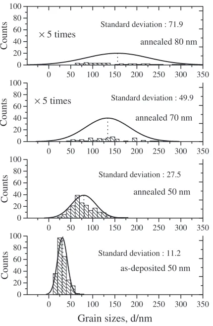
[image:3.595.306.549.71.316.2] [image:3.595.63.276.71.230.2] [image:3.595.47.291.298.403.2]Figure 7 shows a normal distribution of grain sizes of 50-, 70- and 80-nm-wide Cu interconnects plotted as a histogram before and after annealing at 400C for 0.5 h. The grain sizes
were obtained from the identified grain boundaries and computed assuming the grains to be circular, as shown in Fig. 4. The observed length is 4mmfor each interconnects. More than 240 grains were measured from the as-deposited 50-nm Cu interconnect, and 188, 58, and 45 grains were
measured for annealed 50-, 70-, 80-nm-wide Cu intercon-nects, respectively. Twins were not considered to be grain boundaries.
The grain size distribution in the trench of each inter-connect can be determined by comparing the standard deviation of normal distributions. The value of standard deviation for as-deposited 50-nm-wide Cu interconnects is 11.1 with a sharp normal distribution. After annealing, the standard deviation increases to 27.5 in the 50-nm Cu interconnects, and achieves a larger grain size microstructure than in the as-deposited Cu interconnect. As the line widths increase, the standard deviation of 70- and 80-nm Cu interconnects increases to 49.9 and 71.9, respectively. This indicates that the normal distributions become broader and that there are larger ranges of grain size as line width increases. That standard deviations decrease as line width decreases can be attributed to the fact that grain size is constrained by the narrower line width.
Figure 8 shows the average grain size of 50-, 70- and 80-nm-wide Cu interconnects obtained from the measurements shown in Fig. 7. Average grain size increases as line width increases. The average grain size of the 50-nm-wide Cu interconnects grew to 80 nm and was 2.5 times the size of the grains in the 50-nm as-deposited Cu interconnect.
The resistivity of 50-, 70- and 80-nm-wide Cu intercon-nects was plotted against average grain size in Fig. 9. It can be seen that resistivity increases linearly with decreasing line width. This increase is mainly attributed to the density of grain boundary increasing with line widths that are com-parable to the mean free path of electron (39 nm), which causes the electron scattering to occur at the grain boundaries of narrower Cu interconnects. To develop Cu interconnects with low resistivity, coarsening the grain size in narrow Cu interconnects is essential to lowering the resistivity.
4. Conclusion
The grain sizes, grain size distributions and resistivity of 50-nm-wide Cu interconnects in the longitudinal direction were evaluated and compared with those of 70- and 80-nm-wide Cu interconnects to develop a grain size coarsening process. Grain length increases with distance from the bottom
0 40 60 80 100 120 140 160 180 200 80 nm 50 nm
Distance from bottom of trench, d/nm
A
v
erage grain length, l/nm
300 250 200 150 100 50
Fig. 6 Average grain length distribution of 50- and 80-nm-wide, 300-nm-high Cu interconnects after annealing at 400C for 0.5 h. Grain length increased as distance from bottom of trench increased.
0 20 40 60 80 100
Standard deviation : 71.9
as-deposited 50 nm
Grain sizes, d/nm
Counts Counts Counts Counts 0 0 20 40 60 80 100
Standard deviation : 49.9
annealed 50 nm
0 0 20 40 60 80 100
Standard deviation : 27.5
annealed 70 nm
0 20 40 60 80 100
Standard deviation : 11.2
annealed 80 nm
350 300 250 200 150 100 50
0 50 100 150 200 250 300 350
350 300 250 200 150 100 50
0 50 100 150 200 250 300 350
× 5 times × 5 times
Fig. 7 Normal distribution of grain sizes for as-deposited 50-nm Cu interconnect and 50-, 80-nm-wide Cu interconnects are plotted as a histogram. Observed length is 4mmfor each interconnect.
0 20 40 60 80 100 120 140 160 180 200 70 range (48~262) Annealed
134
Annealed Annealed No Anneal50 50 80
range (67~333) range (25~175)
156
80
range (10~60)31
A verage grain size, d/nm
Line width, w/nm
[image:4.595.61.278.71.236.2] [image:4.595.320.534.73.239.2] [image:4.595.64.279.299.627.2]of the trench, and Cu grains inside the trench may have difficulty growing because of the strong restrictions created by the trench geometry. The value of standard deviation in the normal distribution histogram for 50-nm wire was found to be much smaller than those for the 70- and 80-nm Cu wires after annealing. This implies that sufficient grain growth should not be expected in the very narrow Cu interconnect (less than 50 nm) of the future if conventional annealing process is used.
Acknowledgments
This research was supported by NEDO and Grants-in-Aid for Scientific Research. We express our sincere thanks to Mr. H. Miyamoto of Hitachi Kyowa Engineering Ltd., who did the TEM observation.
2) K. Hinode, Y. Hanaoka, K. Takeda and S. Kondo: Jpn. J. Appl. Phys. 40(2001) L1097–L1099.
3) W. Steinho¨gl, G. Schindler, G. Steinlesberger and M. Engelhardt: Phys. Rev. B66(2002) 075414.
4) G. Steinlesberger, M. Engelhardt, G. Schindler and W. Steinho¨gl: Solid-State Electron47(2003) 1233–1237.
5) G. Steinlesberger, M. Engelhardt, G. Schindler, W. Steinhogl, A. V. Glasow, K. Mosig and E. Bertagnolli: Microelectron. Eng.64(2005) 409–416.
6) C.-U. Kim, J. Park, N. Michael, P. Gillespie and R. Augur: J. Electron Mater.32(2003) 982–987.
7) W. Wu, S. H. Brongersma, M. Van Hove and K. Maex: Appl. Phys. Lett.84(2004) 2838.
8) K. Mirpuri and J. Szpunar: Micron35(2004) 575.
9) H. J. Lee, D. I. Kim, J. H. Ahn and D. N. Lee: Thin Solid Films474 (2005) 250.
10) W. Steinho¨gl, G. Schindler, G. Steinlesberger, M. Traving and M. Engelhardt: J. Appl. Phys.97(2005) 023706.
11) M. Moriyama, K. Matsunaga, T. Morita, S. Tsukimoto and M. Murakami: Mater. Trans.45(2004) 3033.
12) S. M. Rossnagel and T. S. Kuan: J. Vac. Sci. & Tech. B: Micro-electronics and Nanometer Structures22(2004) 240.
13) Y. Hirose, N. Hashikawa, K. Fukumoto and Y. Mashiko: J. Electron Microscopy53(2004) 567.
14) K. P. Khoo, J. Onuki, T. Nagano, Y. Chonan, H. Akahoshi, T. Tobita, M. Chiba, T. Saito and K. Ishikawa: Jpn. J. Appl. Phys.45(2006) L852–L853.
15) K. P. Khoo, J. Onuki, T. Nagano, Y. Chonan, H. Akahoshi, T. Tobita, M. Chiba, T. Saito and K. Ishikawa: Advanced Metallization Confer-ence, Tokyo, September (2006) 58.
16) T. Ritzdorf, L. Graham, S. Jin, C. Mu and D. Fraser: IEEE Proc. Int’l Interconnect Tech. Conf., (1998) 106–108.
17) W. Wu, D. Ermur, S. H. Brongersma, M. Van Hove and K. Maex: Microelectron. Eng.76(2004) 190–194.
60 3.0 3.2 3.4 3.6 3.8 4.0
Resisti
vity
,
(
cm)
µ
Ω
Average Grain Size (nm)
80 nm 70 nm
180 160 140 120 100 80
[image:5.595.64.276.72.234.2]