Three-Dimensional Planar Metallic Lenses Based on
Concentric Rings with Modulated Subwavelength Width
Di Feng1,2, Chunxi Zhang1, Lishuang Feng1, Yuanhong Yang1
1School of Instrumentation Science and Optoelectronics Engineering, Beihang University, Beijing, China; 2State Key Laboratory of
Millimeter Waves, Southeast University, Nanjing, China. Email: [email protected]
Received October 7th, 2012; revised November 6th, 2012; accepted November 25th, 2012
ABSTRACT
A kind of Subwavelength Planar Metallic Lenses (SPMLs) is proposed to realize far-field optical focusing in the visible range based on concentric rings with modulated width in a silver film. The width of each metallic ring is mutative so that the radiation fields of surface plasmon polaritons can be controlled and the relevant phase retardations can be modulated to make a beam focus at the desired position. For comparison, the Subwavelength Planar Dielectric Lenses (SPDLs) structured on silica glass with the same concentric ring shapes as SPMLs are analyzed, although without opaque metal coating on SPDLs, the computational results show that SPMLs can support higher intensity focal spot, narrower full-width half-maximum beam width, and longer depth of focus at the focal region under certain lens thick- ness due to the coupling of surface plasomon polaritons, diffracted evanescent waves and propagated electromagnetic waves.
Keywords: Subwavelength Structures; Focus; Surface Plasmons; Diffractive Lenses
1. Introduction
Metallic nanostructures have been a subject of consider- able interest in recent years, since the discovery of ex- traordinary optical transmission phenomena through sub- wavelength metallic aperture array [1,2]. Such light transmission phenomena may be explained as an excita- tion of a Surface Plasmon Polaritons (SPPs) mode which is an electromagnetic excitation existing on the surface of noble metals at the nano-scale aperture entrance where electromagnetic wave propagates through it before emit- ting into radiation modes at the exit [3-5]. Otherwise, with developments of nanofabrication techniques, such as la- ser beam writing, electron beam lithography, and focused ion beam etching, nano-scale metallic structures with high refinement are available. This has enabled to develop new nanophotonic integrated devices based on the plas- monic behavior of metals used for wave guiding, bio- sensing, and superfocusing, etc. [6,7]. In general cases, light can be focused by dielectric optical elements, such as refractive lenses, diffractive lenses, etc, but due to the diffraction of light wave, the resolution of a dielectric lens is limited to about half of the working wavelength. Driven by the potential applications in higher resolution imaging and microscopy, higher density optical data storage, and optoelectronics integrated devices, etc, and
[14], this method still increases the burden for design and fabrication of lenses. In our previous study, we analyzed focusing characteristics of one-dimensional planar di- electric lenses with binary subwavelength structures based on the electromagnetic theory in detail [15]. This Sub- wave-length Planar Dielectric Lenses (SPDLs) can focus light beam quite well and satisfy the planar micro or nano lithographic process. Little work, however, has been done on analyzing focusing characteristics of two-dimen- sional Subwavelength Planar Metallic Lenses (SPMLs) with the same structures as the SPDLs.
So, in this paper, we present the rigorous electromag- netic analysis and design of SPMLs based on concentric nano-rings with modulated width by using 3-D finite- difference time-domain method [16]. The focusing cha- racteristics of planar lenses with nano-scale rings which have the same depth but tuning widths, for linear polari- zation illumination and for different material (metal sli- ver and dielectric silica) have been investigated and com- pared. The simulation results indicate that using the de- sign method of SPDLs, SPMLs can indeed be employed in focusing light in the visible range. The comparative results have shown that when the thickness is less than 200 nm, though SPMLs have opaque silver film and SPDLs are etched on the glass substrate without opaque parts, SPMLs will still support higher intensity focal spot with narrower Full-Width Half-Maximum (FWHM) beam width and longer depth of focus at the focal region since the propagation constants of SPPs and relative phases in metallic rings are strongly dependent on the rings’ width and film’s thickness. When the thickness is larger than 200 nm, the loss of metal will increase, so SPDLs will have better focal performances than those of SPMLs. This ability to manipulate a beam of light in the visible range on the nano-scale metal rings can improve the qua- lity of systems in applications such as photonic and plas- monic integrated devices, optical data storage, sensing and imaging, etc.
This paper is organized as follows: In Section 2 we discuss the basic formulas used in our study, and de- scribe subwavelength structures of SPMLs. In Section 3 we provide and compare results of rigorous designs and analysis of SPMLs and SPDLs with different thicknesses in detail. Finally, a brief conclusion and our contribution are given in Section 4.
2. Theoretical Background and Structure
2.1. Basic Formulas
In our earlier work [15], to a conventional diffractive lens, we approximated its continuous profile to a piece- wise-linear profile, and then encoded the individual lin- ear segments as binary subwavelength structures, so a
Subwavelength Planar Dielectric Lens (SPDL) will be made. In a geometrical argument, the phase delay as a function of radius r from the center of a lens can be ob- tained readily according to the equal optical length prin- ciple:
2 2
0
2π
r n f f r
(1)
where λ0 is the wavelength of light in free space, n the
refractive index of air and f is the focal length of a lens. According to this phase distribution, for the normal inci- dence, the lens will have a continuous surface-relief pro- file, and then this profile can be approximated by linearly increasing widths of a subwavelength planar feature. Al- though SPDLs using this technique can provide good focusing performances, they contain small subwavelength feature sizes and large aspect ratios (ratio of minimum feature height to width) that make them difficult to fa- bricate. So in this paper, we use this technique to make the profile (concentric rings with modulated width) of SPDLs and SPMLs, but the thickness of lens is less than a micrometer.
2.2. Description of Subwavelength Structures
[image:2.595.331.507.494.695.2]A schematic of a subwavelength planar lens is shown in
Figure 1, where D is the diameter of the lens, and t is the
thickness of the planar lens. The material of lens can be silver film or silica dielectric film, and outside the lens is air. From the cross section profile along the x-x plane (as shown in Figure 1(b)), we can see the lens consists of
many Ag/Air/Ag waveguide (like a metal-insulator-metal (MIM) structure) array or Silica/Air/Silica waveguide
(a)
(b)
array with fixed thickness and tuning width. Each indi- vidual silver ring’s width is smaller than the incident wavelength; thus it can be treated as a plasmonic wave- guide. As an incident electromagnetic wave meets the ring, it will be converted into SPPs mode, and transmit- ted along the waveguide, and then decoupled back to an electromagnetic mode with a phase delay upon exiting the ring (a lens’s exiting plane). The complex propaga- tion constant β, which is related to the phase change of the electromagnetic wave after it passes through the ring structure, can be expressed as [17,18]:
2 2
0
2 2 2 2
0 0
tanh d 2
m d d
k w k k m
(2)
where k0 = 2π/λ0 is wave vector of light in free space, and
εm and d are the relative dielectric constant of the
metal medium and the dielectric inside the ring (in this study εd = 1 for air), and w is the ring width. The real and imaginary parts of the effective refractive index neff, de- fined to be β/k0, determine the phase velocity and the
propagation loss of the SPP modes, respectively. Besides, the previous researches have shown that the electric field relative phase at the center of the metal groove exit should be a function of groove depth [12]. So the disper- sion relation between the effective refractive index, rela- tive phase, and ring structures implies that the phase de- lay can be modulated by tuning both ring width and depth.
2
d n
3. Numerical Results and Discussion
In this paper, the three-dimensional electromagnetic dif- fraction problem in a system of a planar lens is sche- matically shown in Figure 1. For SPMLs, we use silver,
and for SPDLs, we use silica glass. The two sides of the lens is air. All of the simulation used the three-dimen- sional finite-difference time-domain method, and the boundary condition is set to the perfect matching layers. The wavelength of incident linear polarized light is 633 nm, and in the visible light range, silver has a negative dielectric constant [19], and the glass has a positive di- electric constant. So the used metal is Ag with εm =
−15.924 + i1.076, and the relative dielectric constant of the used dielectric SiO2 is 2.126 at the wavelength of 633
nm, respectively.
3.1. Numerical Results
The parameters of the lens are as follows: the diameter of the lens D = 8 μm, the designed focal length f = 1.6 μm and the thickness of rings t = 200 nm. The maximum ring size and the minimum ring size are 600 nm, and 50 nm,
respectively. Accordingly, the maximum air width and the minimum one are 300 nm, and 60 nm, respectively. In this study, we define the Depth of Focus (DOF) as a region over which the intensity is greater than 80% of the maximum intensity along the optical axis, and the focal shift (Δf) can be defined as the value that denotes the difference between the position of the maximum irradi- ance position along the light axis and the geometric focal length f (f = 1.6 μm) defined as in Equation (1).
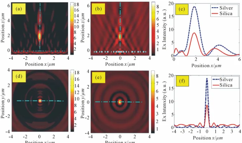
We demonstrate beam focusing by the SPML. The magnitude and profile of electric field intensity focused by the SPML is shown in Figure 2(a), which can give a
global review of focusing characteristics for the SPML. A clear-cut focus appears about 1.88 µm away from the exit surface, which is a little larger than the designed focal length 1.6 µm. This result clearly verifies the feasi- bility of the SPML. Furthermore, Figure 2(b) shows the
profile of electric field intensity focused by the SPDL with the same structure sizes as the SPML, and the focal length is about 1.84 µm. Both the metallic lens and the dielectric lens can focus the light well. Figure 2(d) and (e) show the focal spot intensity along the real focal
plane (z = 1.88 µm for the SPML, and z = 1.84 µm for the SPDL) of the metallic lens and the dielectric lens, respectively. In order to reveal the focusing performance of lenses more clearly, the electric field intensity along z (x = y = 0) direction (the optical axis), and along x (y = 0, z is equal to the real focal position), for the SPDL and the SPML are shown in Figures 2(c) and (f), respectively.
And DOF, the focal shift, FWHM and the Peak value of the SPDL are 0.47 µm, 0.24 µm, 0.42 µm (0.66λ0), and
8.8 units, respectively. The same parameters for the SPML are 0.58 µm, 0.28 µm, 0.31 µm (0.49λ0), and 18.8
units, respectively. It is worth noting that, although there are many opaque metal rings on the SPML, the peak in- tensity of the SPML at the focal plane is much higher than that of the SPDL (about 2.14 times), and also, the FWHM of the SPML is narrower than that of the SPDL (0.31 µm for the SPML, and 0.42 µm for the SPDL, re- spectively). Both the metallic lens and the dielectric lens has the same profile structure and the same ring distribu- tion which means two lenses have the same waveguide structures, but one is a MIM waveguide and the other is a dielectric waveguide. Two lenses are assumed to have 200 nm thickness, and the different thickness will pro- duce different phase delay and the loss, so will have an important influence on the focal performances.
3.2. Comparison of Results
Figure 2. Electric field intensity distributions |Ex|2 for different subwavelength lenses: (a) For the SPML in xz plane; (b) For the SPDL in xz plane; (c) Axial |Ex|2 distributions along z (x = y = 0) direction; (d) For the SPML in xy plane (z = 1.88 µm); (e) For the SPDL in xy plane (z = 1.84 µm); and (f) |Ex|2 distributions along x direction at the real focal plane for SPML and SPDL, respectively. The gray rectangular blocks drawn in (a) are the cross section of the SPML, and the cyan ones drawn in (b) are the cross section of the SPDL, respectively.
using Ag film and SiO2 film whose thicknesses change
from 50 to 400 nm, with 50 nm space. Figures 3(a) and (b) depict the axial |Ex|2 distributions along z (x = y = 0)
direction, and transverse |Ex|2 distributions along x direc-
tion at the real focal plane from SPMLs with various thickness of silver, respectively. And Figures 3(c) and (d)
depict the axial |Ex|2 distributions and transverse |Ex|2
distributions along x direction at the real focal plane from SPDLs with various thickness of silica, respectively. It is obviously seen that there are certain distinctions for dif- ferent thickness and different material, respectively.
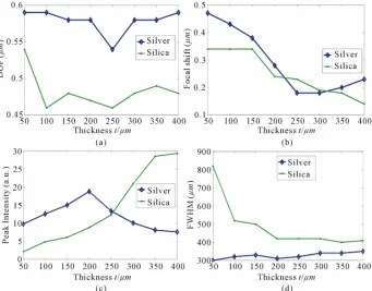
To denote these distinctions more clearly, relevant analysis parameters, such as DOF, the focal shift, FWHM, and the peak intensity have been plotted as a function of thickness, as shown in Figures 4(a)-(d). It is
observed from Figure 4(a) that the deviation of DOF
shows little librations with different film thickness, and DOF of silver lenses are larger than those of silica lenses, which means SPMLs are more suitable for high-precision optical alignment systems, etc. Figure 4(b) shows that
when increasing film thickness, the focal shift will de- crease and the real focal length will be close to the de- signed value. To these phenomena, we think, to both kinds of lenses, there are many subwavelength profiles on the silver film or the silica film, and they form many nano waveguide structures, where electromagnetic waves will produce a complex coupling effect among SPPs, dif- fracted evanescent waves and propagated electromag-
netic waves. When we increase the thickness, the length of waveguide will also increase, so the focal shift will decrease. But for SPMLs, due to SPPs and loss of metal, when the thickness is larger than 250 nm, the focal shift will increase a litter with increasing silver thickness. This can also explain the phenomenon in Figure 4(c), which
shows that when increasing silica thickness, the peak intensity increases for SPDLs, but the peak intensity of SPMLs increases firstly, and when thickness is larger than 200 nm, the peak intensity of SPDLs will decrease with increasing silver thickness. To SPMLs, when thick- ness is under a certain value, the loss of metal will be low, and the coupling effect among SPPs, evanescent waves and propagated waves will play a main role for lens per-formances, and get a better focusing behavior with higher peak value and a narrower FWHM (as shown in Figure 4(d)), but when the thickness is larger enough (for exam-
Figure 3. The electric field intensity distribution in cross sections of the focus alone the z direction (a) and x direction at the real focal plane (b), with different silver thickness for SPMLs, and the electric field intensity distribution in cross sections of the focus alone the z direction (c) and x direction at the real focal plane (d), with different silica thickness for SPDLs, under the illumination of 633 nm plane wave.
Figure 4. The focusing characteristics of SPDLs (Silica) and SPMLs (Silver) as a function of thickness: (a) DOF; (b) Focal hift; (c) Peak intensity; (d) FWHM.
[image:5.595.129.470.439.706.2]
According to analysis results mentioned above, it is evident that SPMLs can indeed get better focusing per- formances and have the advantages of better spatial re- solution (narrower FWHM), larger peak intensity, and longer DOF than SPDLs under certain lens thickness.
4. Conclusion
In conclusion, we have present a kind of Subwavelength Planar Metallic Lenses (SPMLs) to realize far-field optical focusing in the visible range. The SPML is designed based on the conventional Subwavelength Planar Dielec- tric Lens (SPDL), and has concentric rings with modu- lated width in the silver film. The focusing characteristics, such as DOF, the focal shift, FWHM, and the peak inten- sity, of both planar silver lenses and planar silica lenses, have been analyzed with the same rings structure and different film thickness. Compared with the SPDL that is no opaque coating, the SPML can support higher inten- sity focal spot, narrower full-width half-maximum beam width, and longer depth of focus at the focal region under certain lens thickness due to the coupling of SPPs, dif- fracted evanescent waves and propagated electromag- netic waves. It is clear that this kind of new SPMLs may have a good potential for applications in surface optical and optoelectronic integration systems, photonic and plas- monic integrated devices, etc.
5. Acknowledgements
This research is supported by Open Research Fund of State Key Laboratory of Millimeter Waves (K201217) and by Specialized Research Fund for the Doctoral Pro- gram of Higher Education (20091102120020).
REFERENCES
[1] T. W. Ebbesen, H. J. Lezec, H. F. Ghaemi, T. Thio and P. A. Wolff, “Extraordinary Optical Transmission through Sub- wavelength Hole Arrays,” Nature, Vol. 391, 1998, pp. 667-669.
[2] L. Martin-Moreno, F. J. Garcia-Vidal, H. J. Lezec, K. M. Pellerin, T. Thio, J. B. Pendry and T. W. Ebbesen, “The- ory of Extraordinary Optical Transmission through Sub- wavelength Hole Arrays,” Physical Review Letters, Vol. 86, No. 6, 2001, pp. 1114-1117.
doi:10.1103/PhysRevLett.86.1114
[3] L. Martin-Moreno, F. J. Garcia-Vidal, H. J. Lezec, A. De- giron and T. W. Ebbesen, “Theory of Highly Directional Emission from a Single Subwavelength Aperture Sur- rounded by Surface Corrugations,” Physical Review Let- ters, Vol. 90, No. 16, 2003, pp. 167401-167403. doi:10.1103/PhysRevLett.90.167401
[4] W. Srituravanich, L. Pan, Y. Wang, C. Sun, D. B. Bogy and X. Zhang, “Flying Plasmonic Lens in the Near Field for High-Speed Nanolithography,” Nature Nanotechno-
logy, Vol. 3, 2008, pp. 733-737.
[5] H. J. Lezec, A. Degiron, E. Devaux, R. A. Linke, L. Martin- Moreno, F. J. Garcia-Vidal and T. W. Ebbesen, “Beaming Light from a Subwavelength Aperture,” Science, Vol. 297, No. 5582, 2002, pp. 820-822.
doi:10.1126/science.1071895
[6] J. H. Rice, “Beyond the Diffraction Limit: Far-Field Fluo- rescence Imaging with Ultrahigh Resolution,” Molecular
Biosystems,Vol. 3, No. 11, 2007, pp. 781-793.
doi:10.1039/b705460b
[7] N. Fang, H. Lee, C. Sun and X. Zhang, “Sub-Diffraction- Limited Optical Imaging with a Silver Superlens,” Sci- ence, Vol. 308, No. 5721, 2005, pp. 534-537.
doi:10.1126/science.1108759
[8] Y. Fu, W. Zhou, L. E. N. Lim, C. L. Du and X. G. Luo, “Plasmonic Microzone Plate: Superfocusing at Visible Regime,” Applied Physics Letters, Vol. 91, 2007, pp. 61124-61126.
[9] R. G. Mote, S. F. Yu, B. K. Ng, W. Zhou and S. P. Lau, “Near-Field Focusing Properties of Zone Plates in Visible Regime—New Insights,” Optics Express, Vol. 16, No. 13, 2008, pp. 9554-9564. doi:10.1364/OE.16.009554
[10] Y. Liu, Y. Q. Fu, X. L. Zhou, Z. W. Xu, F. Z. Fang and X. T. Hu, “Experimental Study of Indirect Phase Tuning- Based Plasmonic Structures for Finely Focusing,” Plas-
monics,Vol. 6, No. 2, 2011, pp. 227-233.
doi:10.1007/s11468-010-9192-1
[11] H. F. Shi, C. T. Wang, C. L. Du, X. G. Luo, X. C. Dong and H. T. Gao, “Beam Manipulating by Metallic Nano- Slits with Variant Widths,” Optics Express, Vol. 13, No. 18, 2005, pp. 6815-6820. doi:10.1364/OPEX.13.006815 [12] H. F. Shi, C. L. Du and X. G. Luo, “Focal Length Modu-
lation Based on a Metallic Slit Surrounded with Grooves in Curved Depths,” Applied Physics Letters,Vol. 91, No. 9, 2007, pp. 9311-9313.
[13] L. Verslegers, P. B. Catrysse, Z. F. Yu, J. S. White, E. S. Barnard, M. L. Brongersma and S. H. Fan, “Planar Lenses Based on Nanoscale Slit Arrays in a Metallic Film,” Nano
Letters, Vol. 9, No. 1, 2009, pp. 235-238.
doi:10.1021/nl802830y
[14] Q. Chen, “A Novel Plasmonic Zone Plate Lens Based on Nano-Slits with Refractive Index Modulation,” Plasmo- nics, Vol. 6, No. 2, 2011, pp. 381-385.
doi:10.1007/s11468-011-9214-7
[15] D. Feng, Y. B. Yan, G. F. Jin and S. S. Fan, “Beam Fo- cusing Characteristics of Diffractive Lenses with Binary Subwavelength Structures,” Optics Communications,Vol. 239, No. 4-6, 2004, pp. 345-352.
doi:10.1016/j.optcom.2004.05.050
[16] A. Taflove, “Computational Electrodynamics: The Finite- Difference Time-Domain Method,” Artech House, Bos- ton, 1995.
[17] Z. Sun and H. K. Kim, “Refractive Transmission of Light and Beam Shaping with Metallic Nano-Optic Lenses,”
Applied Physics Letters, Vol. 85, 2004, pp. 642- 644.
Express,Vol. 13, No. 6, 2005, pp. 1933-1938. doi:10.1364/OPEX.13.001933
[19] E. D. Palik, “Handbook of Optical Constants of Solids II,” Academic Press, Boston, 1991.
[20] D. Feng, N. F. Song, L. S. Feng, P. Ou and C. X. Zhang,
“Generation of an Extended Depth of Focus Using Dif- fractive Micro-Lenses with Binary Structures in the Non- Paraxial Domain,” Journal of Optics A: Pure and Applied
Optics, Vol. 11, No. 6, 2009, p. 65704.