Solid-state bonding of bulk PbTe to Ni electrode for
thermoelectric modules
FERRERES, Xavier, GAZDER, Azdiar, MANETTAS, Abdrew and
AMINORROAYA YAMINI, Sima <http://orcid.org/0000-0002-2312-8272> Available from Sheffield Hallam University Research Archive (SHURA) at: http://shura.shu.ac.uk/18445/
This document is the author deposited version. You are advised to consult the publisher's version if you wish to cite from it.
Published version
FERRERES, Xavier, GAZDER, Azdiar, MANETTAS, Abdrew and AMINORROAYA YAMINI, Sima (2018). Solid-state bonding of bulk PbTe to Ni electrode for
thermoelectric modules. ACS Applied Energy Materials.
Copyright and re-use policy
See http://shura.shu.ac.uk/information.html
Sheffield Hallam University Research Archive
1
Solid-state bonding of bulk PbTe to Ni electrode
for thermoelectric modules
Xavier Reales Ferreres1
, Azdiar Gazder2
, Andrew Manettas1
, Sima Aminorroaya Yamini1,3*
Australian Institute for Innovative Materials (AIIM), Innovation Campus, University of
Wollongong, Squires Way, North Wollongong , NSW 2500 , Australia
Electron Microscopy Centre (EMC), Innovation Campus, University of Wollongong, Squires
Way, North Wollongong, NSW 2500, Australia
Department of Engineering and Mathematics, Sheffield Hallam University, City Campus,
Sheffield S1 1WB, UK, S.Aminorroaya@shu.ac.uk
ABSTRACT:
The efficiency of thermoelectric generators is defined by the thermoelectric performance of
materials, as expressed by the thermoelectric figure-of-merit, and their contacts with
electrodes. Lead chalcogenide thermoelectric materials, and in particular PbTe, perform well
in the 500 - 900 K temperature range. Here, we have successfully bonded bulk PbTe to Ni
electrode to generate a diffusion barrier, avoiding continuous reaction of the thermoelectric
legs and conducting electrodes at the operating temperature. We have modified the
commonly used spark plasma sintering assembly method to join Ni electrode to bulk PbTe by
driving the total supplied electrical current through the Ni and PbTe solid interfaces. This
2 comprised of nickel telluride. This new technique towards the bonding of PbTe with the
electrode is beneficial for thermoelectric materials, since high temperatures have proven to be
damaging to the quality of bulk material. The interphase microstructure, chemical
composition, and crystallographic information were evaluated by a scanning electron
microscope equipped with electron back-scattered diffraction analysis. The obtained phase at
the Ni/PbTe contact is found to be β2 Ni3±xTe2 with a basic tetragonal crystallographic
structure of the defective Cu2Sb type.
KEYWORDS:
Solid-state bonding, spark plasma sintering, thermoelectric module, PbTe, Nickel electrode
1. INTRODUCTION
Recently, matters related to global warming have drawn attention worldwide 1,2
motivating
sustainable energy projects 3 in order to address a possible future energy crisis 4. Herein,
thermoelectric devices have grown in importance 5
, despite the fact that only low-temperature
applications (up to 473 K) have been successfully commercialised 6
. Thermoelectric device
efficiency and power output increase with temperature 7
, indicating the need to reach higher
temperatures, for instance 500 to 900 K, where lead chalcogenides and PbTe in particular are
known to perform well 6,8
. This could take the technology into significant energy production,
for example, in terrestrial applications, such as combustion engines in vehicles 9,10
, industrial
plants 11
, or concentrating solar thermoelectric generators 12
. Despite the excellent
thermoelectric figure-of-merit (zT) values for PbTe in both n- and p-type compounds 13-18
, the
performance of a device greatly depends on the quality of the junctions between the
thermoelectric material and the metallic electrodes 19,20
. An example of such is the latest study
on PbTe module which is bonded to Cu electrode through a Co0.8Fe0.2 interphase achieving at
3 In order to achieve good contact between materials, the junction must fulfil requirements
such as mechanical stability, and homogeneity of the generated intermetallic. In our recent
study, we have successfully bonded nickel electrode directly to n-type PbTe powder, where a homogenous diffusion barrier of 27 µm composed of nickel telluride was fabricated using the
common spark plasma sintering (SPS) technique 22
. Nevertheless, tuning of the interphase
thickness using the “one-step sintering” method 22 proved to be challenging, since the use of
powder material in any electrical-current-based sintering process facilitates diffusion of
elements 23
, which, in this specific case, resulted in the formation of a thick interlayer at the
contact. The control of interphase geometry is essential to the design of a thermoelectric
generator (TEG) that is capable of achieving maximum power output and conversion
efficiency at working temperatures 24,25. In the current study, we investigate the possibility of
generating an effective bond between bulk p-type PbTe to Ni plate when reducing the thickness of the generated diffusion barrier layer.
Spark plasma sintering apparatus was employed to join solid p-type PbTe bulk to Ni plate. The bonding of thermoelectric materials using SPS with different types of electrodes has
been widely studied in recent years 22,26-28
, although this sort of equipment was initially
designed for the consolidation of powder. Both processes commonly entail the use of a
graphite die, which is employed as housing for the powders. The intrinsic electrical current in
any SPS process is distributed between the powder undergoing sintering and the graphite die
throughout the entire time for the procedure. This distribution depends not only on the
sample’s electrical conductivity but on the different interface resistances appearing during the
complex process of powder consolidation at the stages of heating, sintering, and cooling in
the SPS. Other potential issues caused by the die-sample current distribution are seen as
radial temperature gradients across the specimen, as well as localized Joule heating due to
large current densities at the contact between the sample and the graphite die 23
4 cause even higher temperatures when joining two dissimilar materials with possible issues of
sample melting. Moreover, the lower electrical resistance of graphite die at higher
temperatures compared to that of PbTe, increases the complexity of current distribution
across the assembly in the case of bonding two dissimilar materials. An effect of complex
distribution of electrical current on the quality of sintered samples has been previously
highlighted 29. Therefore, in order to simplify our bonding assembly, we avoided the graphite
die by using bulk PbTe instead of powder in order to force the total supplied current to pass
through the PbTe and Ni, eliminating the possible interaction of the current with the die.
Nevertheless, a large release of heat will still occur in the contact area between the Ni and the
PbTe due to high current densities resulting from point contacts originating from the surface
roughness of the materials 30.
This method resulted in the formation of a thin and homogenous interphase layer of β2
phase nickel telluride (Ni3±xTe2). A detailed analysis of the crystallographic structures at the
Ni/PbTe interface was conducted, which showed the appearance of ordered superstructures of
the β2 nickel telluride phase.
2. MATERIALS AND METHODS
Polycrystalline samples of Pb0.985Na0.015Te were synthesized by mixing the stoichiometric
ratio of high purity Pb (99.999%), Te (99.999%), and Na in vacuum-sealed quartz ampoules.
Samples were heated to 1373 K and homogenised for 10 hours, followed by quenching in
cold water. Afterwards, the samples were annealed at 823 K for 72 hours. The resulting
ingots of p-type PbTe were hand-ground to powder with an agate mortar and a pestle. The obtained powder was consolidated into disks 12 mm in diameter and 1.5 mm thick using a
Thermal Technology LLC, Model 10-4 Spark Plasma Sintering (SPS) apparatus at 793 K and
5 The Seebeck coefficient and electrical resistivity of samples were measured using Linseis
LSR-3 apparatus. The thermal conductivity (κ) was calculated from 𝜅=𝜌𝐷!𝐶!. The laser
flash method (Linseis LFA 1000) was used to measure the thermal diffusivity (DT). The
density (ρ) was calculated using the measured weight and dimensions, and the specific heat
capacity (Cp) was estimated by Cp = 3.07 + 4.7 × 10 -4
× (T[K] – 300) 31,32
.
The spark plasma sintering equipment is used to join the solid p-type PbTe bulk materials to Ni plates. This method can be described as solid-state interdiffusion bonding, where the
thermocouple readings are used to adjust the system supplied electrical current in order to
control the temperature for bonding. The SPS apparatus provided a pulsed DC current, which
passed through both solid materials and the mating surfaces of PbTe and Ni. These surfaces
were polished down to a roughness of 1 µm and ultrasonically cleaned with ethanol prior to
the joining process in order to remove any possible contaminants. The pre-bonding
thicknesses of the PbTe and Ni disks were approximately 1.5 mm and 0.3 mm, respectively.
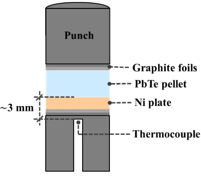
To proceed with the bonding, the assembly is sandwiched between layers of graphite foil
inside the SPS chamber so to improve the thermal contact and distribution of force given by
the graphite punches. The schematic illustration in Figure 1 shows the absence of a graphite
die, therefore exposing the peripheral surfaces of PbTe and Ni to the chamber’s atmosphere
during the process of bonding. As a result, a possible radial variation in the interphase
thickness could occur, which can be due to a temperature gradient in the sample’s diameter
caused by the increase in heat radiation loss when compared to the usage of a graphite die 23.
The temperature and holding time for the SPS procedure were optimised to achieve ideal
bonding parameters, but nonetheless, the heating and cooling rates remained constant at 5
6 Figure 1. Experimental assembly for bonding between PbTe and Ni solids.
The thermal stability of PbTe sample after bonding to Ni plate was studied. The
measurement of thermoelectric transport properties of the sample prior to bonding to Ni and
after bonding was performed by mechanically removing the Ni plate and generated interphase
using Struers Tegramin-20 automatic polisher. The electrical conductivity and Seebeck
coefficient were measured using Linseis LSR-3 apparatus.
The electrical resistance of the interphase was measured using the Quantum Design PPMS
equipment. Samples after performance of SPS bonding process were utilized for this purpose.
The I-V curve was obtained to determine the ohmic contact resistance of Ni to p-type PbTe. Electrical currents below 100 mA were used to avoid Joule heating in the samples during
measurement, while frequencies of 100 Hz were set to avoid Peltier effect. The final
resistance value of interphase and contacts is obtained by subtracting the resistance values of
PbTe and Ni from the total resistance of Ni+PbTe sample.
In order to study the microstructure of the interphase, joint samples were cut using Leica
TXP Target Polisher equipment. Subsequently, cross-sections were mounted in conductive
7 was used down to 1 µm, and the fine polished surfaces were prepared for electron
back-scattered diffraction (EBSD) using ion milling on a Leica TIC-020.
EBSD results were obtained from a 69 × 13.5 µm2
area using a JEOL JSM-7001F field
emission-scanning electron microscope (SEM) operating at 15 kV, a roughly 6.5 nA probe
current, and 1500× magnification. The microscope used a Nordys-II EBSD detector with
Oxford Instruments Aztec software as interface. The conditions for EBSD mapping were
previously calculated with 44, 42, and 40 reflectors employed for Ni, Ni3Te2 (virtual
tetragonal), and PbTe phases, respectively, as well as 4×4 binning, 1 background frame, a
Hough resolution of 60, and simultaneously indexed individual Kikuchi patterns up to 6
bands. The overall indexing rate for the raw EBSD map was 99%. The step size employed
was 0.06 µm, which was equivalent to a map resolution of 1150 × 225 pixels.
4. RESULTS AND DISCUSSION
The interface temperature and the holding time for bonding are crucial parameters for the
final quality of joint materials. We have optimised the joining temperature, holding time, and
pressure to effectively bond p-type PbTe to Ni electrode. It is worth noting that similarity on coefficients of thermal expansion (CTE) between bonded materials is essential to avoid, at
high temperature, strain to failure of bonded region. The CTE of PbTe (20 𝑥 10-6
K-1
)33
and Ni
(13.4 𝑥 10-6
K-1
) have shown to reasonably withhold at high temperatures 22,34
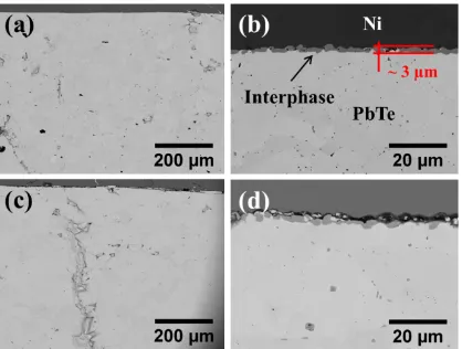
8 Figure 2. SEM micrographs of bonding areas at the PbTe/Ni interface after sintering under
pressure of 20 MPa for 5 minutes (a, b), and 15 minutes (c, d) at temperature 623 K.
Figure 2(a) and (b) shows SEM micrographs of the fabricated interphase between PbTe and
Ni plate, generated by sintering at 623 K, 20 MPa for 5 minutes. Figure 2(b) delineates a new
phase at the PbTe/Ni interface, indicating the occurrence of a reaction between the initial
counterparts. The thus-formed interphase presents no major signs of cracks or defects, similar
to the PbTe side of the sample (Figure 2(a)). The average thickness of the interlayer is
approximately 3 µm, and the discontinuity in the morphology is unwanted for application in a
thermoelectric module. The lack of a defined barrier layer could lead to instability of the
junction due to Ni diffusion into PbTe 35
or vice versa at the operating temperature of the
device. Therefore, in order to increase the fabricated thickness and thus obtain a more
homogeneous diffusion layer, the holding time for bonding was increased to 15 min (Figure
2(c) and (d)). The microstructure of the newly obtained interphase shows no improvement,
indicating that time has, in this case, no significant effect on the thickness. In addition, the Ni
and the intermediate layer are physically separated (Figure 2(d)), and there is also a
significant amount of cracking on the PbTe side (Figure 2(c)). This suggests that during the
Ni/PbTe reaction the holding time is a critical factor for the quality of bonding and the
9 The reaction occurring between Ni and PbTe is represented in chemical Equation (1), as is
discussed in our recent study 22
, which presents solid nickel telluride and liquid lead as the
reaction products.
(3±x)Ni s +2PbTe s →Ni!±!Te! s +2Pb l (1)
Theoretical thermodynamic calculations based on chemical Equation (1) have identified
793 K as the temperature for spontaneous reaction (Gibbs free energy, ΔG < 0) 22
.
Experiments undertaken in the current study, however, indicate that 623 K is sufficient to
initiate the solid-state reaction between Ni and PbTe (Figure 2). Given such realization, it is
important to emphasise that the disparity between temperatures could be due to the extra
amount of radiation loss coming from the sample’s surface at the periphery in the newly
proposed SPS assembly compared to our previous report 22
,where the usage of a graphite die
and its enveloping insulation prevented such losses from occurring. Additionally, the distance
of roughly 3 mm between the end of the thermocouple and the Ni/PbTe reaction area,
illustrated in Figure 1, is also a key factor for the experimental temperature reading due to the
heat conduction through the bottom graphite punch. This separation was also presented in our
recent study 22
, suggesting that the sample’s surface exposure in the current SPS assembly is
[image:10.595.188.400.550.655.2]also a cause for the low temperature read by the thermocouple.
Figure 3. One-dimensional thermal model for the bonding process of current assembly in the
10 A one dimensional thermal model was performed (Figure 3) to determine the sample’s
temperature (Ts) (detailed in Supporting information). Figure 3 presents a schematic graph of
the modelled assembly, which corresponds to half of the total SPS assembly due to its
horizontal symmetry across the center of the Ni+PbTe sample. This model includes heat
radiation from the sample and graphite punch as well as the heat conducted from the sample
to the area where the thermocouple tip is located, which is at an exact distance of d = 3.2 mm.
Equations 2, and 3 present the heat balance for the model. The supplied power by surface
area (P/A), defined as Psupplied, is half of the averaged value for peaks of power during the 5
minutes of sintering (see Figure S2 and S3 of Supporting information). The emissivity values
for graphite (εGraphite)and lead telluride (εPbTe) are 0.95 36
and 0.9837
, respectively. Whereas, the
conductivity coefficient for HPD grade graphite, provided by the supplier (kGraphite)
corresponds to 85 Wm-1
K-1
. It is assumed that the temperature of contact between sample and
graphite punch is the same and equal to Ts, eliminating the heat conduction along the PbTe +
Ni assembly. This approximate model highlights the significant difference of bonding
temperatures between the current study and the theoretical temperature of formation for
Ni3Te2 (793 K).
P!"##$%&' =q!"#$%!&'"#+q!"#,!"#$ (!!)+q!"#,!"#$%&'( (!∗) (2)
P A=
k!"#$%&'(
d T!−T!" +ε!"#$ σ T!! −T!! +ε!"#$%&'( σ T∗ ! −T
!! (3)
The average power for sample in Figure 2(b), at 623 K, corresponds to 426.55 W (Figure
S2) which leads to a Ts of 764 K using Equation 3. This calculated temperature is lower than
the theoretical temperature of formation for Ni3Te2, though this disparity is likely to be
originated from the small quantity of nickel telluride generated at the contact (Figure 2(b)).
11 interphase evolution as a function of temperature and to maintain a constant experimental
[image:12.595.192.402.127.343.2]temperature during the holding process.
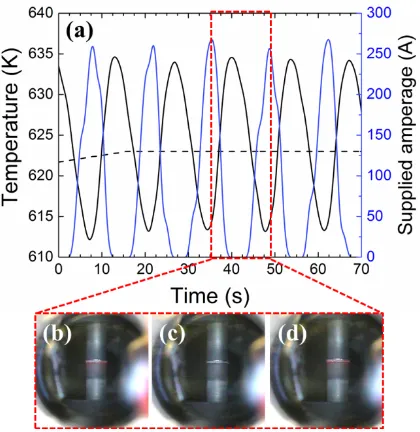
Figure 4. (a) SPS parameters of electric current (blue solid line), thermocouple temperature
(black solid line), and temperature set point (black dashed line) during the holding time for
the bonding procedure for the sample at 623 K, 20 MPa for 5 minutes; (b), (c), (d) frames
extracted from a video of the bonding process, showing a red glow during spikes of supplied
current.
Figure 4(a) presents the measured temperature, set point temperature, and supplied electric
current at the beginning of the SPS holding time for the sample shown in Figure 2(a) and (b).
The electric current is supplied via the equipment’s proportional, integral, derivative (PID)
process controller, using the measured temperature as the input variable to regulate the
heating of assembly according to the pre-defined SPS program. The solid line for the
measured temperature in Figure 4(a) shows constant fluctuations of ±20 K from the defined
temperature set-point (dashed line), suggesting that the current PID settings struggle with the
fast released heat at the Ni/PbTe interface, thus resulting in large oscillations of electrical
12 process, we have monitored the assembly during the bonding process (Figures 4(b) to (d)).
The interface of PbTe/Ni glows red at the maximum peaks of current, with periodic cycles of
14 seconds, indicating that during oscillations of roughly 280 A (blue line) the interface
temperature is ~ 900 K, when radiation becomes visible with wavelengths in the 700 nm
region 38
. This suggests that the reaction shown in Equation (1) occurs during the peaks of
current and that the short reaction times are not sufficient to generate a thick diffusion layer.
Therefore, higher temperature, implying more current in the system via the PID controller,
might be necessary to obtain a thicker diffusion barrier, since longer time has proven to be
inefficient. Figures 2(c) and (d) shows that such oscillations in the current over an extended
period of time have a significant effect on the quality of the interface, resulting in the
[image:13.595.198.406.382.538.2]separation of layers.
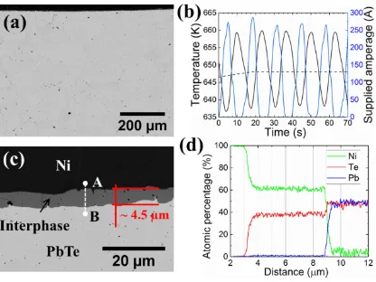
Figure 5. (a) SEM image of bonded sample generated during SPS bonding at 648 K, 20 MPa,
and 5 minutes; (b) SPS parameters of supplied electrical current, thermocouple temperature,
and temperature set-point illustrated by the blue solid line, the black solid line, and the black
dashed line, respectively, for the same conditions expressed in (a); (c) higher magnification
SEM micrograph of the sample in (a) to observe the thickness of the interphase; (d) line scan
13 Figure 5 shows the fabrication of interphase by increasing the bonding temperature, from
623 K (Figure 2) to 648 K, and consequently, the amplitude of oscillations in the electric
current (Figure 5(b)). The sample temperature was approximated at 792.7 K through the
model presented in Figure 3 and calculated using Equation 3 with a supplied power of Psupplied
= 438.75 W. A homogeneous reaction layer is formed at the interface between Ni and PbTe
when they are bonded at 20 MPa for 5 minutes (Figure 5(c)). The generated interphase is
roughly 4.5 µm thick and free of large porosity or cracks, indicating good cohesion between
the layers. In addition, the distinct separation of the Ni electrode from the PbTe by the
interlayer suggests the formation of an effective diffusion barrier. Figure 5(b) shows peaks of
current close to 300 A, meaning that there was an increase on temperature due to more Joule
heating than in the previous samples, these higher currents aid the Ni/PbTe reaction to form a
thicker barrier layer. This and a visual analysis during the experimental process show that
temperatures around 900 K were only generated at the contact and that the bulk of the PbTe
was exposed to lower temperatures. This is viewed as an improvement of the new technique
that promotes the bonding of PbTe with the electrode, since temperatures above 773 K have
been proven to damage the quality of the bulk material.
Figure 5(d) show a line scan taken from point A to point B in Figure 5(c) which confirms
no diffusion of elements in Ni and PbTe and a clear chemical separation of the
Ni/interphase/PbTe phases. It also indicates that the interphase is solely composed of Ni and
Te elements. The atomic percentage of Te element (roughly 38%) is indicative of the
formation of a β2 Ni3±xTe2 phase 39
. The formation of β2 phase Ni3±xTe2 together with the
absence of Pb at the contact are similar findings to those in our previous report on bonding of
Ni plate to n-type PbTe powder using SPS 22. Therefore, these results suggest strong thermal
stability of the interphase when exposed to the operating temperature of the device.
14 were measured to assess the thermal stability of PbTe during bonding procedure. Figure 6(a)
and (b) show that the electronic transport properties of samples remain roughly the same after
bonding process, indicating the joining method preserves the performance of thermoelectric
material.
Figure 6. (a) Seebeck coefficients and (b) electrical conductivities of p-type PbTe samples
before (solid symbols) and after (open symbols) SPS bonding with Ni electrode.
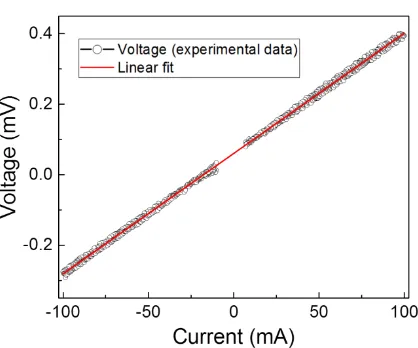
The electrical resistance for p-type PbTe bulk was measured at 1.36 mΩ, using measured room temperature resistivity of material and sample’s dimensions, whereas the total
resistance for the Ni+PbTe sample was 3.24 mΩ, calculated by the slope of Figure 7 (V-I
curve), showing an ohmic behavior of bonded sample. The electrical resistance for Ni3Te2
and interface contacts with Ni and PbTe is of 1.87 mΩ, using a theoretical resistance of 3.2 x
10-3
[image:15.595.86.512.180.355.2]15 Figure 7. Experimental data (open symbols) for V-I curve of p-type PbTe bond to Ni plate and linear fit (solid line) indicating ohmic contact between the parts
The crystallographic structure of the interphase layer between Ni and PbTe was
investigated using combined energy dispersive X-ray spectroscopy (EDS) and electron
back-scattering diffraction (EBSD). The EDS results obtained from area maps and analysis of 20
random points within the interphase shows an average chemical composition of: Ni (at. %
61.92 ± 0.4687), and Te (at. % 38.08 ± 0.4687), indicating a chemical composition of
Ni3.3Te2. This suggests that the interphase layer is solely composed of β2 phase Ni3±xTe2 which
nominally ranges in composition from Ni0.61Te0.39 to Ni0.59Te0.41 39
. The Ni3.3Te2 phase has been
described as having a monoclinic crystal symmetry, with corresponding lattice parameters a
= 7.54 Å, b = 3.799 Å, c = 6.089 Å, and β = 91.2º 40
, and with having the lowest enthalpy of
formation for the three possible β2 Ni3±xTe2 phases 41
, hence being the stable compound at
room temperature. Nevertheless, it is important to note that the monoclinic structure
commonly ascribed to Ni3Te2 in previous studies is formed from a basic tetragonal of the
defective Cu2Sb-type 40
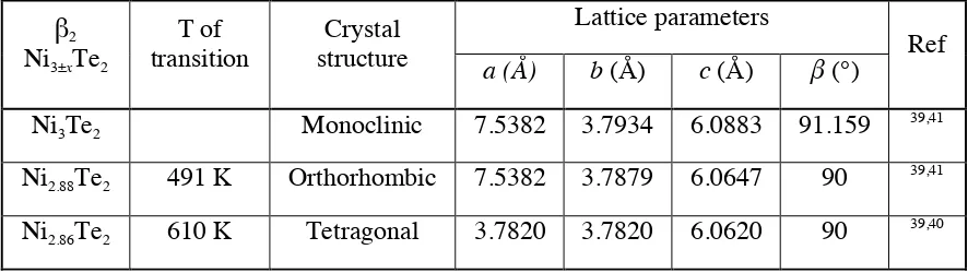
. Table 1 summarises the existing β2 phases of Ni3±xTe2, as well as the
transition temperatures within the phase: from monoclinic to orthorhombic 42
to tetragonal 43
.
16 ordering of Ni atoms in the asymmetric unit cell 40
, in addition to the close proximity of the
[image:17.595.76.519.194.319.2]lattice parameters of the phases.
Table 1. β2 phase of Ni3±xTe2 with the corresponding crystallographic structures, lattice
parameters, and their transition temperatures.
β2
Ni3±xTe2
T of transition Crystal structure Lattice parameters Ref
a (Å) b (Å) c (Å) β(°) Ni3Te2 Monoclinic 7.5382 3.7934 6.0883 91.159
39,41
Ni2.88Te2 491 K Orthorhombic 7.5382 3.7879 6.0647 90
39,41
Ni2.86Te2 610 K Tetragonal 3.7820 3.7820 6.0620 90
39,40
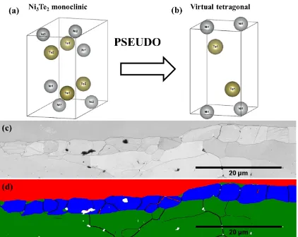
Figures 8(c) and (d) show the EBSD band contrast and phase distribution maps,
respectively. Figure 8(d) illustrates top layer comprising large Ni grains (shown in red),
whereas the middle and bottom layers contain multigrain Ni3Te2 (shown in blue), and PbTe
(shown in green) phases, respectively. The non-indexed regions, shown in white in Figure
8(d), represent voids and porosities. It is worth noting that when the Ni3Te2 phase was first
indexed as a monoclinic phase (Figure 8(a)), some grains presented with fictitious boundaries
within grain interiors with angle-axis 90º/<001>, 180º/<100>, and 180º/<001>. These
fictitious boundaries are representative of pseudo-symmetry in this phase which is caused by
the mis-indexing of the monoclinic electron back-scattering patterns 44
.
The detection of pseudo-symmetry in monoclinic Ni3Te2, is beneficial in that it predicts the
possible phase transitions as well as the existence of a virtual parent structure 45
. These are in
agreement with the particular case of the nickel telluride system, where the aforementioned
ordering of Ni cations within the lattice gives rise to a structural relationship between
high-temperature tetragonal and room-high-temperature monoclinic nickel telluride. In order to
17 Bilbao Crystallographic server) was used to: (i) identify possible pseudo-symmetries in
crystal structures and thereafter, (ii) calculate a virtual parent of a higher symmetry based on
the minimum atomic displacement of the unit cell 45
. Consequently, the PSEUDO program
checks if every atomic position in an initially defined crystal structure belonging to a lower
symmetry space group can be described by a virtual crystal structure corresponding to a
higher symmetry through small displacements to new atomic positions. In the present case of
nickel telluride, the pseudo-symmetry in the monoclinic phase of space group 11 can be
adequately described as a virtual tetragonal phase, space group 129 (shown in Figure 8(b)).
Figure 8(d) shows phase distribution map when Ni3Te2 is indexed as a virtual tetragonal
(129) crystal structure. The interphase layer presents with no pseudo-symmetry whatsoever.
It is to note that twins represented in red appear in the interphase and have 82.5º <110>
18 Figure 8. (a) Crystallographic structure for monoclinic Ni3Te2 (b) Tetragonal crystal structure
assigned as the virtual parent of structure (a) obtained via PSEUDO program in order to
detect and remove pseudosymmetry. (c) EBSD band contrast map, (d) EBSD phase
distribution map with grain boundaries and twins using virtual tetragonal structure of (b).
4. CONCLUSIONS
The successful bonding of bulk p-type single-phase PbTe and Ni plate was achieved using a modified assembly method on a common type of SPS apparatus. Eliminating the graphite
die during sintering forced the supplied electrical current to pass through the interface of the
solids. The formation of a continuous and defect free interphase layer was obtained as thin as
4.5 µm when compared to then roughly 27 µm using powder PbTe together with a graphite
die. This improvement is achieved due to consistent surface roughness of mating surfaces,
19 interphase layer is composed of solely monoclinic β2 phase Ni3±xTe2. The observed
pseudosymmetry at some grains during EBSD analysis suggested the existence of a virtual
parent crystal with tetragonal symmetry, similar to the high temperature tetragonal Ni2.86Te2.
This derived virtual tetragonal, with space group 129, shows higher indexation during EBSD,
allowing for the study of the correct orientation of boundaries in the interphase layer.
ASSOCIATED CONTENT
Supporting Information
Additional details on the thermal model; equation for heat losses; power supplied by SPS
during sintering of samples.
AUTHOR INFORMATION
Corresponding Author
*Email: S.Aminorroaya@shu.ac.uk (S.A.Y.)
Notes
The authors declare no competing financial interest. ACKNOWLEDGMENTS
This work was supported by an Australian Research Council (ARC) Linkage Project
(LP120200289), an ARC Discovery Early Career Research Award (DE130100310), and the
AutoCRC 2020 (Project Agreement 1-203). The authors would like to thank the Electron
Microscopy Centre (EMC) at the University of Wollongong for offering access to
microscopes and sample preparation equipment.
REFERENCES
1 Peters, G. P.;Marland, G.;Le Quéré, C.;Boden, T.;Canadell, J. G.;Raupach, M. R.
20 2 Cook, J.;Oreskes, N.;Doran, P. T.;Anderegg, W. R. L.;Verheggen, B.;Maibach, E.
W.;Carlton, J. S.;Lewandowsky, S.;Skuce, A. G.;Green, S. A. Consensus on consensus: a
synthesis of consensus estimates on human-caused global warming. Environmental Research Letters2016, 11, 048002.
3 Ellabban, O.;Abu-Rub, H.;Blaabjerg, F. Renewable energy resources: current status,
future prospects and their enabling technology. Renewable and Sustainable Energy Reviews
2014, 39, 748-764.
4 Qureshi, M. I.;Rasli, A. M.;Zaman, K. Energy crisis, greenhouse gas emissions and
sectoral growth reforms: Repairing the fabricated mosaic. Journal of Cleaner Production
2016, 112, 3657-3666.
5 Zheng, X. F.;Liu, C. X.;Yan, Y. Y.;Wang, Q. A review of thermoelectrics research–
Recent developments and potentials for sustainable and renewable energy applications.
Renewable and Sustainable Energy Reviews2014, 32, 486-503.
6 Snyder, G. J.;Toberer, E. S. Complex thermoelectric materials. Nature Materials
2008, 7, 105-114.
7 Rowe, D. M. CRC Handbook of Thermoelectrics: Macro to Nano,CRC Taylor & Francis, 2006.
8 Fitriani;Ovik, R.;Long, B. D.;Barma, M. C.;Riaz, M.;Sabri, M. F. M.;Said, S.
M.;Saidur, R. A review on nanostructures of high-temperature thermoelectric materials for
21 9 Qiang, J. W.;Yu, C. G.;Deng, Y. D.;Su, C. Q.;Wang, Y. P.;Yuan, X. H.
Multi-objective optimization design for cooling unit of automotive exhaust-based thermoelectric
generators. Journal of Electronic Materials2016, 45, 1679-1688.
10 Ibrahim, E. A.;Szybist, J. P.;Parks, J. E. Enhancement of automotive exhaust heat
recovery by thermoelectric devices. Proceedings of the Institution of Mechanical Engineers, Part D: Journal of Automobile Engineering2010, 224, 1097-1111.
11 Ebling, D. G.;Krumm, A.;Pfeiffelmann , B.;Gottschald, J.;Bruchmann, J.;Benim, A.
C.;Adam, M.;Labs, R.;Herbertz, R. R.;Stunz, A. Development of a system for thermoelectric
heat recovery from stationary industrial processes. Journal of Electronic Materials2016, 45, 3433-3439.
12 Kraemer, D.;Jie, Q.;McEnaney, K.;Cao, F.;Liu, W.;Weinstein, L. A.;Loomis, J.;Ren,
Z.;Chen, G. Concentrating solar thermoelectric generators with a peak efficiency of 7.4%.
Nature Energy2016, 1, 16153.
13 Heremans, J. P.;Jovovic, V.;Toberer, E. S.;Saramat, A.;Kurosaki,
K.;Charoenphakdee, A.;Yamanaka, S.;Snyder, G. J. Enhancement of thermoelectric
efficiency in PbTe by distortion of the electronic density of states. Science 2008, 321, 554-557.
14 Androulakis, I.;Todorov, I.;Chung, D. Y.;Ballikaya, S.;Wang, G.;Uher, C.;Kanatzidis,
M. High thermoelectric efficiency in co-doped degenerate p-type PbTe. MRS Proceedings
2010, 1267.
15 Vineis, C. J.;Shakouri, A.;Majumdar, A.;Kanatzidis, M. G. Nanostructured
22 16 Biswas, K.;He, J.;Blum, I. D.;Wu, C. I.;Hogan, T. P.;Seidman, D. N.;Dravid, V.
P.;Kanatzidis, M. G. High-performance bulk thermoelectrics with all-scale hierarchical
architectures. Nature2012, 489, 414.
17 LaLonde, A. D.;Pei, Y.;Snyder, G. J. Reevaluation of PbTe1-xIx as high performance
n-type thermoelectric material. Energy & Environmental Science2011, 4, 2090-2096.
18 Zhao, L. D.;Dravid, V. P.;Kanatzidis, M. G. The panoscopic approach to high
performance thermoelectrics. Energy & Environmental Science2014, 7, 251-268.
19 Kim, Y.;Yoon, G.;Park, H. S. Direct Contact Resistance Evaluation of Thermoelectric
Legs. Experimental Mechanics2016, 56, 861-869.
20 Xia, H.;Drymiotis, F.;Chen, C. L.;Wu, A.;Chen, Y. Y.;Snyder, G. J. Bonding and
high-temperature reliability of NiFeMo alloy/n-type PbTe joints for thermoelectric module
applications. Journal of Materials Science2015, 50, 2700-2708.
21 Hu, X.;Jood, P.;Ohta, M.;Kunii, M.;Nagase, K.;Nishiate, H.;Kanatzidis, M.
G.;Yamamoto, A. Power generation from nanostructured PbTe-based thermoelectrics:
comprehensive development from materials to modules. Energy & Environmental Science
2016, 9, 517-529.
22 Reales Ferreres, X.;Aminorroaya Yamini, S.;Nancarrow, M.;Zhang, C. One-step
bonding of Ni electrode to n-type PbTe–a step towards fabrication of thermoelectric
generators. Materials & Design2016, 107, 90-97.
23 Guillon, O.;Gonzalez-‐Julian, J.;Dargatz, B.;Kessel, T.;Schierning, G.;Räthel,
23 materials, and technology developments. Advanced Engineering Materials 2014, 16, 830-849.
24 Rowe, D. M.;Min, G. Evaluation of thermoelectric modules for power generation.
Journal of Power Sources1998, 73, 193-198.
25 Bjørk, R. The universal influence of contact resistance on the efficiency of a
thermoelectric generator. Journal of Electronic Materials2015, 44, 2869-2876.
26 Fan, J.;Chen, L.;Bai, S.;Shi, X. Joining of Mo to CoSb3 by spark plasma sintering by
inserting a Ti interlayer. Materials Letters2004, 58, 3876-3878.
27 de Boor, J.;Gloanec, C.;Kolb, H.;Sottong, R.;Ziolkowski, P.;Müller, E. Fabrication
and characterization of nickel contacts for magnesium silicide based thermoelectric
generators. Journal of Alloys and Compounds2015, 632, 348-353.
28 Kraemer, D.;Sui, J.;McEnaney, K.;Zhao, H.;Jie, Q.;Ren, Z. F.;Chen, G. High
thermoelectric conversion efficiency of MgAgSb-based material with hot-pressed contacts.
Energy & Environmental Science2015, 8, 1299-1308.
29 Locci, A. M.;Cincotti, A.;Todde, S.;Orrù, R.;Cao, G. A methodology to investigate
the intrinsic effect of the pulsed electric current during the spark plasma sintering of
electrically conductive powders. Science and technology of advanced materials2010, 11. 30 Kazakov, N. F. Diffusion bonding of materials.,Mashinostroenie, 1981.
31 Blachnik, R.;Igel, R. Thermodynamische Eigenschaften von IV–VI-Verbindungen:
Bleichalkogenide/thermodynamic properties of IV–VI-compounds: Leadchalcogenides.
24 32 Pashinkin, A. S.;Mikhailova, M. S.;Malkova, A. S.;Fedorov, V. A. Heat capacity and
thermodynamic properties of lead selenide and lead telluride. Inorganic Materials2009, 45. 33 Hikage, Y.;Masutani, S.;Sato, T.;Yoneda, S.;Ohno, Y.;Isoda, Y.;Imai, Y.;Shinohara,
Y. 26th International Conference on Thermoelectrics. 331-335.
34 Xia, H.;Drymiotis, F.;Chen, C. L.;Wu, A.;Snyder, G. J. Bonding and interfacial
reaction between Ni foil and n-type PbTe thermoelectric materials for thermoelectric module
applications. Journal of Materials Science2014, 49, 1716-1723.
35 George, T. D.;Wagner, J. B. Diffusion of nickel and chlorine into lead telluride II.
diffusion at the phase limits. Journal of The Electrochemical Society1969, 116, 848-854. 36 Fuschillo, N.;Gibson, R. Germanium-silicon, lead telluride, and bismuth telluride
alloy solar thermoelectric generators for venus and mercury probes. Advanced Energy Conversion1967, 7, 43-52.
37 Neuer, G. Spectral and total emissivity measurements of highly emitting materials.
International Journal of Thermophysics1995, 16, 257-265.
38 Tipler, P. A.;Meyer-Arendt, J. R. College physics. Applied Optics1987, 26, 5220. 39 Ball, R. G. J.;Dickinson, S.;Cordfunke, E. H. P.;Konings, R. J. M.;Drowart, J.;Smoes,
S. (Commission of the European Communities, 1992).
40 Kok, R. B.;Wiegers, G. A.;Jellinek, F. The system nickel-‐tellurium I. Structure and
some superstructures of the Ni3±qTe2 phase (preliminary communication). Recueil des
Travaux Chimiques des Pays-Bas1965, 84, 1585-1588.
41 Gulay, L. D.;Olekseyuk, I. D. Crystal structures of the compounds Ni3Te2, Ni3−δTe2
25 42 Grønvold, F. Heat capacities and thermodynamic properties of hexagonal and liquid
selenium in the range 298 to 1000 K. Enthalpy and temperature of fusion. The Journal of Chemical Thermodynamics1973, 5, 525-531.
43 Mills, K. C. Heat capacity of nickel and cobalt tellurides. Journal of the Chemical Society, Faraday Transactions 1: Physical Chemistry in Condensed Phases1974, 70, 2224-2231.
44 Karthikeyan, T.;Dash, M. K.;Saroja, S.;Vijayalakshmi, M. Evaluation of misindexing
of EBSD patterns in a ferritic steel. Journal of microscopy2013, 249, 26-35.
45 Capillas, C.;Tasci, E. S.;de la Flor, G.;Orobengoa, D.;Perez-Mato, J. M.;Aroyo, M. I.
A new computer tool at the bilbao crystallographic server to detect and characterize