Theoretical study of tunneling current in the access region of various
heterojunction field-effect transistor structures
Philippe Jansen,a)Hiroshi Mizuta, and Ken Yamaguchi
Hitachi Ltd., Central Research Laboratory, 1-280 Higashi-koigakubo, Kokubunji-shi, Tokyo 185, Japan
Mathias Wagner
Hitachi Cambridge Laboratory, Madingley Road, Cambridge CB3 0HE, United Kingdom ~Received 21 November 1994; accepted for publication 14 December 1995!
The source resistance of a heterojunction field-effect transistor ~HFET!, whose reduction is mandatory for high-performance devices, consists of an ohmic contact resistance and an access resistance. The access region is located between the geometrical source and the geometrical source side of the gate contact. By means of a quantum-mechanical modeling program, the effect of changes in layer structure in the access region of a HFET is studied. A new heterojunction structure using a Si planar doped layer is designed to improve the linearity and reduce the access resistance by more than ten times for a specific transistor layout. Thanks to the higher sensitivity of the modeling program to structural information, the contribution of the tunneling current and the change of equilibrium as a function of temperature is investigated. © 1996 American Institute of Physics.
@S0021-8979~96!00307-6#
I. INTRODUCTION
In recent years, heterojunction field-effect transistors
~HFETs!with ever increasing performances have been fabri-cated thanks to improvements in layer structure, layer growth, use of planar or delta-doped layers, and reduction of the source resistance.1The reduction of the source resistance is mandatory for high-performance HFETs as this resistance deteriorates the extrinsic transconductance, the maximum os-cillation frequency, and minimum noise figure.2 The source resistance can be commonly divided into two parts. The first part is the contact resistance which carriers experience when they flow from the contacting metal to the semiconductor. The second contribution results from carriers flowing from the ohmic contact region to the source side of the two-dimensional electron gas~2DEG!channel. This second resis-tance is the access resisresis-tance. Recent work has been mainly directed to the improvement of the ohmic contacts and the reduction of the access resistance by source-gate spacing reduction.3,4
The reduction of source-gate spacing is considered to be the most difficult and least reproducible step for high-yield device processing. The conditions for source-gate spacing reduction can however be relaxed by reducing the resistance of the access region. In this article a new structure is pro-posed which leads to a reduction of the access resistance due to enhanced tunneling and increased current density in vari-ous parts of the heterostructure.
A quantum-mechanical modeling program5,6 has been used to compare the resistance value and linearity of the current–voltage characteristics with those of several other heterostructures achieving access resistance reduction. To obtain a quantitative description of the contribution of the tunneling current on one side and the thermionic/diffusion current on the other side, the current transport is analyzed as a function of temperature. Moreover, conclusions are drawn
concerning the stability of the structure and its relative inde-pendence from external forces.
II. MODELED STRUCTURES DESIGN
The access resistance in a HFET structure consists in a first approximation of three parallel conduction paths as seen in Fig. 1. These three paths in a standard GaAs/AlGaAs/ InGaAs source contact structure are the highly doped GaAs top layer, the undepleted AlGaAs electron supply layer, and the 2DEG channel. Under the geometric contact at the source we consider these three paths to be shorted. However, at a certain distance from this contact the voltage in the 2DEG channel will rise due to the resistance along the channel and perpendicular to the channel which is mainly determined by tunneling and thermionic emission over the heterojunction diodes.
For optimized structures, however, very little can be done about the resistance of the 2DEG channel, which is optimized toward highest electron density and so to lowest resistance. Although when the resistance across the vertical heterojunction diode is negligible, the total resistance can be reduced by reducing the top-layer resistance. Reduction of the top-layer resistance by replacing GaAs by InyGa12yAs has been described by Kuroda et al.,7 and by inserting an InyGa12yAs quantum well between the electron supply layer and the top layer it has been described in former work.2 These two techniques, however, do not take into account the increase in barrier height of the electron supply layer at the interface with the top layer, due to the larger heterojunction dipole which is created. As the vertical heterojunction diode resistance then becomes significant, the improvement ob-tained by these two techniques remains marginal.
has to be partly removed during the gate etch in order to obtain high-quality Schottky diodes. The new heterostruc-ture, presented here with a single Si planar layer in the top layer, combines the reduction of top layer resistance and of vertical heterojunction diode resistance. To obtain this struc-ture the Si planar doped layer has to be grown in the same material as the top layer at a distance d, not farther from the electron supply layer than given by
0,d5 nd
531018 cm23<30 nm,
with nd the total integrated doping of the Si planar doped layer.
Two fundamental heterostructures chosen from previous research2 are the following. The uniformly doped hetero-structure consists of a 500 nm n1-GaAs layer ~Si, 531018 at. cm23!, a 200 nm n-GaAs layer~Si, 131018 at. cm23!, a 10 nm semi-intrinsic~s.i.!-GaAs layer followed by an 8 nm s.i.-In0.25Ga0.75As quantum well, a 2 nm s.i.-Al0.25Ga0.75As
spacer layer, a 25 nm n1-Al0.25Ga0.75As electron supply layer ~Si, 331018 at. cm23!, 10 nm n2-Al0.25Ga0.75As layer ~Si,
531017 at. cm23!, and finally a 100 nm n1-GaAs top layer
~Si, 531018 at. cm23!. The semi-intrinsic layers are stimu-lated with a 106at. cm23Si doping.
The delta-doped heterostructure consists of a 500 nm
n1-GaAs layer ~Si, 531018 at. cm23!, a 200 nm n-GaAs layer ~Si, 131018 at. cm23!, a 10 nm s.i.-GaAs layer fol-lowed by an 8 nm s.i.-In0.25Ga0.75As quantum well, a 5 nm s.i.-Al0.25Ga0.75As spacer layer, a Si delta-doped layer with density 731012 at. cm22, a 32 nm n2-Al0.25Ga0.75As layer
~Si, 531017 at. cm23!, and finally a 100 nm n1-GaAs top layer ~Si, 531018 at. cm23!. The delta-doped Si layer is de-scribed as a layer with the same characteristics as the sur-rounding layers and the doping density is considered to be spread over 5 nm length.
To study the influence of an InyGa12yAs top quantum
well and the delta-doped layers, the following structures, schematically drawn in Fig. 2, are considered: The first struc-ture is the uniformly doped heterostrucstruc-ture as described above; the second structure has a uniformly doped electron supply layer, as does the first structure, but the top layer contains a 5 nm n1-In0.25Ga0.75 as top quantum well ~Si,
531018 at. cm23! at the edge with the 10 nm
n2-Al0.25Ga0.75As layer; the third structure is the delta-doped
heterostructure as described above, but the top layer contains
a 5 nm n1-In0.25Ga0.75As top quantum well ~Si, 5310 18
at. cm23!at the edge with the 32 nm n2-Al0.25Ga0.75As layer;
the fourth structure is the delta-doped heterostructure, but the top layer contains a delta-doped Si layer with density 731012
at. cm22 at 2.5 nm from the edge with the 32 nm
n2-Al0.25Ga0.75As layer.
III. COMPUTER SIMULATION RESULTS
Using the drift-diffusion and quantum-mechanical mod-eling programs described in previous work,2,5,6 the band structure, carrier density, and resistance of heterostructure diodes are analyzed.
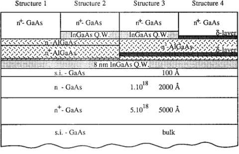
To reduce the access resistance, a new structure, de-scribed as structure 4, is designed, based on the addition of a Si planar doped layer in the cap material, in front of the GaAs/AlGaAs top heterojunction. The vertical and horizon-tal resistance are reduced due to the vanishing of the top heterojunction barrier and due to the higher carrier density in the planar doped layer, respectively. The band diagram of the new heterostructure is obtained by combining the band dia-gram of a conventional delta-doped heterostructure with the one of a single Si planar layer as shown in Fig. 3~a!.
Due to this combination principle, based on the linearity of the Poisson equation towards charge, the location as well as the density of the planar doped layer can be optimized for maximum performance. In Fig. 3~b!it is shown that the po-sition of the Si planar layer can be changed with respect to the AlGaAs/GaAs heterojunction. It is not mandatory to have the planar layer near to the heterojunction to remove the heterojunction barrier. The design window for the location of planar layer, as described previously, is available by adapting the planar layer density. In Fig. 3~c!the carrier density in the structure is shown for the drift-diffusion and quantum-mechanical model simulation. The strong decrease of the car-rier density in the AlGaAs/InGaAs heterojunction barcar-rier, noticed in the drift-diffusion result, is not seen in the quantum-mechanical result as tunneling through this thin barrier is taken into account. The effect of resistance lower-ing by removal of the top heterojunction barrier can only be simulated using the quantum-mechanical modeling program. FIG. 1. Definition of the access region and the three parallel conducting
[image:2.612.319.559.38.193.2]paths which contribute to the access resistance in the HFET layer structure.
[image:2.612.59.283.41.142.2]When using the drift-diffusion model the height of the AlGaAs/InGaAs barrier dominates the transport characteris-tics through the thermionic current equation.
The possibility of placing the Si planar doped layer in the top layer material is crucial for the practical realization of the HFET, which requires a high-quality Schottky diode for the gate. In this new structure a high-quality Schottky diode is obtained by the complete removal of the planar doped layer, together with the cap layer under the gate under stan-dard etching conditions. This new structure can therefore also be used in selective etching processes for HFETs as the barrier material has a different composition than the cap layer material which contains the planar doped layer. The use of a planar doped electron supply layer improves the vertical current even more. Therefore, it is believed that the HFET structure with double planar doping is a good candidate for a minimum access resistance heterostructure.
Using the modified quantum-mechanical modeling program,2the dependency of resistance as a function of ap-plied bias has been studied for a uniformly doped HFET structure and the newly presented structure with planar
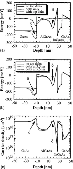
doped electron supply layer and planar doped top layer. The simulations were performed at 77 K. The band diagram and the bound, quasibound, or local states are displayed in Fig. 4. Due to the high barriers in the band diagram of the conven-tional uniformly doped HFET the states are strongly local-ized. In the case of the delta-doped HFET with top delta doping the states are no longer localized due to the removal of the top heterojunction barrier and the reduction of the 2DEG/electron supply layer heterojunction barrier.
[image:3.612.98.252.32.387.2]The access resistance for the structures 1– 4 is shown in Table I. The values for the horizontal conductivity are ob-tained by multiplying the simulated carrier density with the mobility of the respective layers and the electron charge. The vertical resistivity was obtained by quantum-mechanical simulation. The total resistance is a combination of these values. The results clearly show that the total resistance can become considerably smaller than the 2DEG resistance value. From this table, one also notices the bad effect of a high vertical resistance on the total resistance, as for struc-tures 2 and 3. The vertical current density and resistance as a function of bias for structures 1 and 4 are shown in Fig. 5. The vertical resistance of the double delta-doped structure is nearly ten times lower than the resistance of the uniformly doped HFET structure. The standard deviation relative to the mean value for the studied interval~@22 mV,12 mV#!is 7% for the new structure and 45% for the conventional HFET structure. Especially toward the drain side ~positive volt-ages!, very good linearity is obtained. At the source side the linearity is worse due to the saturation of the heterojunction barrier height separating the 2DEG from the supply layer as a function of bias. At high current densities, as observed in FIG. 3. ~a!Combination of a Si planar doped layer~dotted line! with a
[image:3.612.360.515.38.148.2]conventional delta-doped HFET structure ~solid line!. The resulting struc-ture is shown by the dashed line.~b!Band diagram comparison between the conventional delta-doped HFET and the structures with additional Si planar doped layer at 3.5 and 5.5 nm of the heterojunction. ~c! Carrier density calculated by the drift-diffusion model ~solid line! and the quantum-mechanical model~dotted line!.
[image:3.612.314.561.652.739.2]FIG. 4. Band diagram and position of the maxima of the local density of states for the delta-doped HFET structure with additional Si planar top layer on top. The maxima are only given in that part of the structure where the wave function is maximum.
TABLE I. Calculated resistances at 77 K for the three parallel paths assum-ing 2500, 1500, and 20 000 cm2/V s as mobility for the top layer, supply layer, and 2DEG, respectively. The total access resistance is a combination of these parallel paths.
Structure 1 ~mV/mm!
Structure 2 ~mV/mm!
Structure 3 ~mV/mm!
Structure 4 ~mV/mm!
Top layer 122 115 116 102
Supply layer 752 936 921 590
2DEG 124 116 100 94
Vertical 132 234 535 14
the double delta-doped structure, the barrier height causes saturation of the source current, whereas for the conventional structure the expected diode behavior is obtained.
IV. MODELING OF THE TEMPERATURE BEHAVIOR
The modeling of the temperature behavior is an interest-ing way to analyze the rate of tunnelinterest-ing current versus ther-mionic current through the structure. The tunneling current depends mainly on the density of states and depends barely on temperature. The thermionic current, on the contrary, de-pends strongly on temperature and is nonexistent at low tem-peratures when high barriers are to be overcome.
The structure under consideration is a delta-doped HFET with 5 nm In0.25Ga0.75As top quantum well. This structure
was chosen because the top heterojunction barrier prohibits carriers from tunneling through this thick barrier and so re-duces the total current. At room temperature, however, the transport is expected to be mainly thermionic current over the barrier, so the difference between the room and the liquid-nitrogen current is the thermionic current.
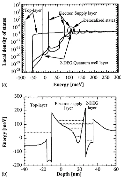
For the analyzed structure, one can see in Fig. 6~a!that the interaction between the 2DEG and the top contact side is very loose, due to the reduced tunneling through the struc-ture. The connection with the back contact is very strong as the local density of states is raised by two decades upon reaching the corresponding energy level~at about 55 meV!. The interaction between the 2DEG and the electron supply layer is strong as can be seen in Fig. 6~b!. This strong inter-action can even contribute to the delocalization of the nor-mally local states. This delocalization or resonance is shown in Fig. 6~b!at an energy of about 106 meV.
When comparing the position of the strongly localized bound and quasibound states with the reference energy cho-sen in the middle between the left- and right-hand-side conduction-band energies, one observes that this position does not change with temperature. The difference in energy between the conduction bands in equilibrium, however, in-creases with temperature and so does the position of the local states. This is in agreement with the theory which claims that the temperature does not affect the already filled states, e.g., the bound and quasibound states, but affects the filling of the states around and above the Fermi level. Although it can be argued that when the position of the conduction bands on either side of the heterostructure moves, the bound and
[image:4.612.337.536.33.322.2]qua-sibound states should follow the changes. It is shown in Fig. 7 that the difference in energy is minimum ~about zero! in the layers which contain the bound ~215 to 210 nm! or quasibound states~17 to 23 nm and 27 to 35 nm!. The posi-tion of these filled states fully determines the equilibrium condition for this structure. The heterojunction FET structure in the access regions is screened off from its contacts and reacts as a closed system to external forces such as current or temperature. These external forces will barely change the equilibrium achieved by the filled states and their interaction. FIG. 5. Current vs potential for a conventional uniformly doped HFET
structure and the delta-doped HFET structure with additional Si planar doped top layer.
[image:4.612.97.252.36.146.2]FIG. 6. ~a!Local density of states as a function of energy for the top layer, electron supply layer, and 2DEG quantum-well layer for a delta-doped HFET structure with top quantum well.~b!Band diagram and position of the maxima of the local density of states for the delta-doped HFET structure with top quantum-well structure. The position of a maximum is only given in that part of the structure where the wave function reaches its maximum.
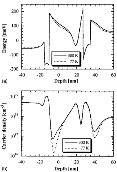
[image:4.612.330.546.559.703.2]The differences in band structure and carrier density can be seen in Figs. 8~a! and 8~b!, respectively. Although few differences can be seen in the plot of the band diagram, major differences are observed for the carrier densities in and around the heterojunction barriers. By thermionic emission the carrier density in the top heterojunction barrier is en-hanced by a factor of 5. The density in the heterojunction barrier between the 2DEG and the GaAs substrate is in-creased by a factor of 2. At the very thin 2DEG/electron supply layer barrier the density is only increased by about 20%, as most current was already tunneling through it.
V. CONCLUSIONS
In this article the influence of the layer structure on ac-cess resistance has been studied using both drift-diffusion and quantum-mechanical models. The addition of a planar doped layer on top of the GaAs/AlGaAs heterojunction im-proved the carrier density in the top layer significantly with-out reduction of the vertical tunneling current. The vertical
current depended strongly on the AlGaAs/2DEG heterojunc-tion barrier height, which can be reduced by using a Si pla-nar doped AlGaAs electron supply layer. A layer structure with planar doped top heterojunction layer and AlGaAs elec-tron supply layer have been shown to be the best structure for low access resistance.
The current–voltage characteristics and the resistance of two realistic diode structures, a conventional uniform doped HFET and a double delta-doped HFET, have been analyzed using a quantum-mechanical simulation model. The latter structure showed a current density across the structure which is a factor of 10 larger than the conventional structure. More-over the analysis of the linearity of the resistance as a func-tion of bias is reduced from 45% for the convenfunc-tional struc-ture to 7% for the double delta-doped strucstruc-ture at 77 K.
The temperature behavior of the heterojunction diodes contributed to the understanding of the physical phenomena occurring in these structures. Increase of the temperature leads to a strong increase of the thermionic/diffusion current over the heterojunction barriers, whereas this current was negligible at liquid-nitrogen temperature. These heterostruc-tures, as they occur in the access region of HFETs, maintain their equilibrium and oppose each change at their contacts. For temperature changes from liquid-nitrogen temperature to room temperature it has been shown that filled bound and quasibound states in the heterostructure determine this equi-librium and that mainly the energy levels of the contact lay-ers have to change to accommodate the difference in struc-tural parameters.
ACKNOWLEDGMENTS
The authors wish to thank Dr. T. Mishima, T. Tanimoto, and K. Higuchi for their helpful discussions.
1See, for instance HEMTs & HBTs: Devices, Fabrication, and Circuits,
edited by F. Ali and A. Gupta~Artech House, Boston, 1991!, pp. 79– 84, or L. D. Nguyen, L. L. Larson, and U. K. Mishra, Proc. IEEE 80, 494 ~1992!; and also Ph. Jansen, Ph.D. thesis, Katholieke Universiteit Leuven, Belgium, 1993.
2Ph. Jansen, H. Mizuta, M. Wagner, and K. Yamaguchi, Tech. Rep. IEICE
ED94-5, 31~1994!. 3
Ph. Jansen, W. De Raedt, M. Van Hove, R. Jonckheere, R. Pereira, and M. Van Rossum, Mater. Res. Soc. Symp. Proc. 181,~1990!.
4Ph. Jansen, Ph.D. thesis, Katholieke Universiteit Leuven, Belgium, 1993. 5M. Wagner, Phys. Rev. B 45, 11 595~1992!.
6M. Wagner, in Proceedings of the Fourth International Symposium on the
Foundations of Quantum Mechanics, Tokyo 1992 @Jpn. J. Appl. Phys.
Series 9, 114~1993!#.
7S. Kuroda, N. Harada, T. Katakami, T. Mimura, and M. Abe, IEEE Trans.
[image:5.612.74.276.30.325.2]Electron Devices ED-36, 2196~1989!. FIG. 8. ~a!Band diagram and~b!carrier density for a delta-doped HFET