ASSEMBLY and TEST INSTRUCTIONS
Processor Technology Corporation
6200Hollis Street
CUTS, COMPUTER USERS TAPE SYSTEM
SECTION
I
II
TITLE
INTRODUCTION and GENERAL INFORMATION 1.1 Introduction • • . • •
1.2 General Information 1.2.1
1.2.2 1.2.3 1.2.4 1.2.5
CUTS Description Receiving Inspection Warranty Information Replacement Parts • Factory Service . . • ASSEMBLY and TEST
2.1 2.2 2.3
Parts and Components . Assembly Tips • • • Assembly Precautions
2.3.1 Handling MOS Integrated 2.3.2 Soldering
· · · ·
2.3.3 Installing and Removing Module. · · ·
·
· · ·
Circuits
· · ·
·
CUTS
· ·
· · ·
2.3.4 Installing and Removing Integrated2.4 2.5 2.6
Circuits
· · · · ·
· ·
· · · ·
2.3.5 Use of Clip Leads· · ·
·
· · ·
Required Tools, Equipment and Materials OrientationAssembly-Test . . . • • • • • 2.6.1 Circuit Board Check • • • • 2.6.2 Assembly-Test Procedure • • III OPTION SELECTION
IV
3.1 3.2 3.3
Option Selection
Port Address Selection (DIP Switch, Sl) Audio Output Selection •
3.4 Data Rate Selection OPERATING PROCEDURES 4.1 Tape Recorder
4.2 CUTS-Recorder Interconnect (Single
·
·
·
·
·
Recorder) • • • • • . . . • • • • • • • • 4.3 CUTS-Recorder Interconnect (Two
Recorders) • • • • . • • • • • •
SECTION IV
V
VI
APPENDICES
TITLE
OPERATING PROCEDURES continued 4.4 Recorder Adjustments .
4.4.1 4.4.2
Volume Control Tone Control
4.5 write Operations . • • • • 4.6 Read Operations
THEORY OF OPERATION 5.1
5.2 5.'3
Introduction .
Block Diagram Analysis . • • • . . • • Theory of Operation • • • • . . . • • • •
5.3.1 Timing • • • • . . • . 5.3.2 Control.. • • • • • •
5.3.3 write Mode . • • • • • • •
5.3.4 Read Mode . • . • • • . • • • . • • DRAWINGS
CUTS Assembly Drawing • CUTS Schematic • • • • • .
I Statement of Warranty II 8080 Operating Codes
III Standard and Tantalum Dipped Capacitor Color Codes
IV Loading DIP Devices, Soldering Tips and Installing Augat Pins
V IC Pin Configurations
i i
IV-2 IV-2 IV-2 IV-4 IV-4
V-I V-I V-2 V-2 V-4 V-6 V-8
CUTS, COMPUTER USERS TAPE SYSTEM TABLES/ILLUSTRATIONS
TABLE 2-1 5-1
FIGURE 2-1 2-2 2-3 4-1 5-1
TITLE
CUTS Parts List . • • • • • • • • Strobe Decoder (U23) Truth Table
TITLE Identification of components Heat sink and U7 installation .
CUTS-transport interconnect cabling • • CUTS-recorder interconnect (two recorders) CUTS simplified block diagram • • • • • • •
PAGE II-2,3
IV-6
PAGE II-4,5
GENERAL INFORMATION
CUTS, COMPUTER USERS TAPE SYSTEM
Processor
Technology
Processor
TechnologyCorporation
CUTS, COMPUTER USERS TAPE SYSTEM SECTION I
1.1 IN'rRODUCTION
This manual supplies the information needed to assemble, test and use the CUTS, Computer Users Tape System. We suggest that you first scan the entire manual before starting assembly. Then, make sure you have all the parts and components listed in the IIParts Listll (Table 2-1) in Section II. When assembling the module, follow the instructions in the order given.
Should you encounter any problem during assembly, calIon us for help if necessary. If your completed module does not work pro-perly, recheck your assembly step by step. Most problems stem from poor soldering, backward installed components, and/or installing the wrong component. Once you are satisfied that the module is correct-ly assembled, feel free to ask for our help.
1.2 GENERAL INFORMATION 1.2.1 CUTS Description
CUTS, The Computer Users Tape System is a high speed, simple to use audio cassette interface that operates at 300 and 1200 bps data rates under program control. The recording technique used is asynchronously Manchester coded at 1200 or 2400 Hz and is CUTS/Byte/ Kansas City Standard compatible.
Two separate tape transport control outputs and two cornmon audio inputs and outputs are provided to drive one or two recorders. In addition, CUTS has provision for selecting
1)
a low level audio output signal for driving the microphone input to an audio recorder, 2) a high level audio output signal for driving the auxiliary input to an audio recorder, and 3) a 5-volt peak-to-peak square save out-put for driving a digital recorder. A fully automatic gain control operates in the read mode. Unlike other cassette interfaces, CUTS has absolutely no critical adjustments that must be preset or adjusted during operation.1.2.2
All Processor Technology software is available on CUTS cassettes at lower cost than equivalent paper tapes. Receiving Inspection
1.2.3 warranty Information
In brief, parts that fail because of defects in materials or workmanship are replaced at no charge for 3 months for kits, and one year for assembled products, following the date of purchase. Also, products assembled by the buyer are warranted for a period of 3 months after the date of purchase; factory assembled units carry a one year warranty. Refer to Appendix I for the complete "Statement of Warranty".
1.2.4 Replacement Parts
Order replacement parts by component nomenclature (DM8131 IC or lN2222 diode, for example) and/or a complete description (680 ohm,
~ watt, 5% carbon resistor, for example). 1.2.5 Factory Service
In addition to in-warranty service, Processor Technology also provides factory repair service on out-of-warranty products. Before returning the unit to Processor Technology, first obtain our authorization to do so by writing us a letter describing the problem. After you receive our authorization to return the unit, proceed as
follows:
1. Write a description of the problem.
2. Pack the unit with the description in a container suitable to the method of shipment.
3. Ship prepaid to Processor Technology Corporation, 6200 Hollis Street, Emeryville, CA 94608.
Your unit will be repaired as soon as possible after receipt and return shipped to you prepaid. (Factory service charges will not exceed $20.00 without prior notification and your approval.)
ASSEMBLY
CUTS, COMPUTER USERS TAPE SYSTEM
Processor
Technology
Processor Technology Corporation
6200 Hollis Street
2.1 PARTS AND COMPONENTS
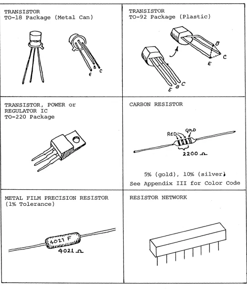
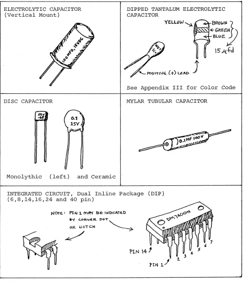
Check all parts and components against the "Parts List" (Table 2-1 on Page 11-2). If you have difficulty in identifying any parts by sight, refer to Figure 2-1 on Page 11-3.
2.2 ASSEMBLY TIPS
1. Scan Section II in its entirety before you start to assemble your CUTS kit.
2. In assembling your CUTS, you will be following a step-by-step assembly procedure. FOLLOW THE INSTRUCTIONS IN THE ORDER
GIVEN.
3. Assembly steps and component installations are pre-ceded by a set of parentheses. Check off each installation and step as you complete them. This will minimize the chances of omitting a step or component.
4. When installing components, make use of the assembly aids that are incorporated on the CUTS PC board and the assembly drawing. (These aids are designed to assist you in correctly in-stalling the components.)
a. The circuit reference (R3, C10 and U7, for example) for each component is silk screened on the PC board near the location of its installation.
b. Both the circuit reference and value or nomenclature (1.5K and 74LS08, for example) for each component are included on the assembly drawing near the loca-tion of its installaloca-tion.
5. To simplify reading resistor values after installation, install resistors so that their color codes read from left-to-right and top-to-bottom as appropriate (board oriented as defined in Para-graph 2.5 on Page 11- .)
6. Unless specified otherwise in the instructions, install components--especially disc capacitors--as close to the board as possible.
7. Should you encounter any problem during assembly, call on us for help if needed.
CUTS, COMPUTER USERS TAPE SYSTEM SECTION II
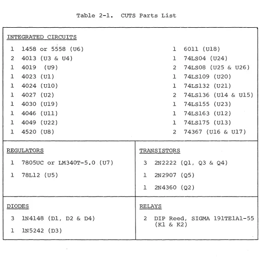
Table 2-1. CUTS Parts List
INTEGRATED CIRCUITS
1 1458 or 5558 (U6) 1 6011 (U18)
2 4013 (U3
&
U4) 1 74LS04 (U24)1 4019 (U9) 2 74LS08 (U25
&
U26)1 4023 (Ul) 1 74LSI09 (U20)
1 4024 (UI0) 1 74LS132 (U21)
1 4027 (U2) 2 74LS136 (U14
&
U15)1 4030 (U19) 1 74LS155 (U23)
1 4046 (Ull) 1 74LS163 (U12)
1 4049 (U22) 1 74LS175 (U13)
1 4520 (U8 ) 2 74367 (U16
&
U17)REGULATORS TRANSISTORS
1 7805UC or LM340T-5.0. (U7 ) 3 2N2222 (Ql, Q3
&
Q4)1 78L12 (U5) 1 2N2907 (Q5)
1 2N4360 (Q2)
DIODES RELAYS
3 lN4148 (Dl, D2
&
D4) 2 DIP Reed, SIGMA 191TEIAl-55(Kl
&
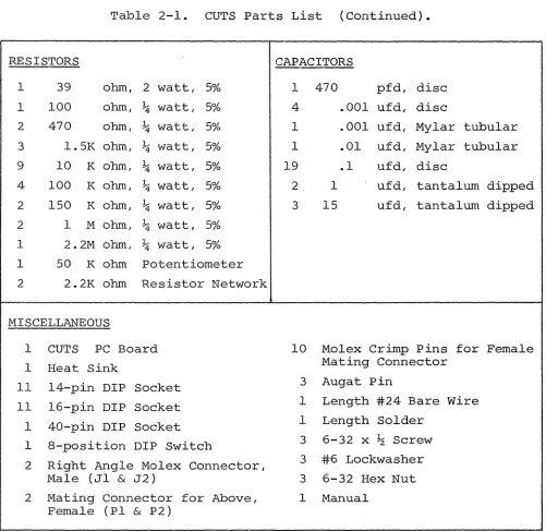
K2) [image:10.612.43.548.90.610.2]Table 2-1. CUTS Parts List (Continued).
RESISTORS CAPACITORS
1 39 ohm, 2 watt, 5% 1 470 pfd, disc 1 100 ohm, ~ watt, 5% 4 .001 ufd, disc
2 470 ohm, ~ watt, 5% 1 .001 ufd, Mylar tubular 3 1.5K ohm, ~ watt, 5% 1 .01 ufd, Mylar tubular 9 10 K ohm, ~ watt, 5% 19 .1 ufd, disc
4 100 K ohm, ~ watt, 5% 2 1 ufd, tantalum dipped 2 150 K ohm, ~ watt, 5% 3 15 ufd, tantalum dipped 2 1 M ohm, ~ watt, 5%
1 2.2M ohm, ~ watt, 5% 1 50 K ohm Potentiometer
2 2.2K ohm Resistor Network
MISCELLANEOUS
1 CUTS PC Board 10 Molex Crimp Pins for Female
1 Heat Sink Mating Connector
11 14-pin DIP Socket 3 Augat Pin
11 16-pin DIP Socket 1 Length #24 Bare Wire 1 40-pin DIP Socket 1 Length Solder
1 8-position DIP Switch 3 6-32 x J..z Screw 2 Right Angle Molex Connector, 3 #6 Lockwasher
Male (Jl
&
J2) 3 6-32 Hex Nut 2 Mating Connector for Above, 1 ManualFemale (PI
&
P2) [image:11.612.69.570.114.601.2]CUTS, COMPUTER USERS TAPE SYSTEM
TRANSISTOR
TO-IS Package (Metal Can)
TRANSISTOR, POWER or REGULATOR IC
TO-220 Package
METAL FILM PRECISION RESISTOR (1% Tolerance)
SECTION II
TRANSISTOR
TO-92 Package (Plastic)
c
CARBON RESISTOR
5% (gold), 10% (silver. See Appendix III for Color Code RESISTOR NETWORK
[image:12.612.55.554.88.671.2]ELECTROLYTIC CAPACITOR (Vertical Mount)
DISC CAPACITOR
Monolythic (left) and Ceramic
DIPPED TANTALUM ELECTROLYTIC CAPACITOR
VEI-LOW ~ BRO~N}
=~::".:~~
GREeN,
BLUE. .'--~
\5"
.t{.+d
See Appendix III for Color Code MYLAR TUBULAR CAPACITOR
INTEGRATED CIRCUIT, Dual Inline Package (DIP) (6,8,14,16,24 and 40 pin)
?tNl..!
Figure 2-1. Identification of componentso
[image:13.612.63.560.108.689.2]CUTS, COMPUTER USERS TAPE SYSTEM SECTION II
2.3 ASSEMBLY PRECAUTIONS
2.3.1 Handling MOS Integrated Circuits
Many of the IC's used in the CUTS are MOS devices. They can be damaged by static electricity discharge. Always handle MOS IC's
so that gQ discharge will flow through the IC. Also, avoid
unneces-sary handling and wear cotton--rather than synthetic-~clothing when handling these IC's.
2.3.2 Soldering **IMPORTANT**
1. Use a fine tip, low-wattage iron, 25 watts maximum.
2. DO NOT use excessive amounts of solder. DO solder neat-ly and as quickneat-ly as possible.
3. Use only 60-40 rosin-core solder. NEVER use acid-core solder or externally applied fluxes.
4. To prevent solder bridges, position iron tip so that i t does not touch adjacent pins and/or traces simultaneously.
5. DO NOT press tip of iron on pad or trace. To do so can cause the pad or trace to "lift" off the board and permanently
damage i t .
6. The flow through to solder bridges. component.
CUTS circuit board has plated-through holes. Solder the component (front) side of the board can produce
Check for such bridges after you install each
7. The CUTS circuit board has an integral solder mask (a lacquer coating) that shields selected areas on the board. This mask minimizes the chances of creating solder bridges during assem-bly. DO, however, check all solder joints for possible bridges.
8. Additional pointers on soldering are provided in Appen-dix III of this manual.
2.3.3 Installing and Removing CUTS Module
NEVER install the CUTS in, or remove i t from the computer with the power on. To do so can damage the module.
2.3.4 Installing and Removing Integrated Circuits.
2.3.5 Use of Clip Leads
NEVER attach clip leads to the top edge of the CUTS PC board. To do so can short the +8, +16 and -12 V dc buses to one another.
2.4 REQUIRED TOOLS, EQUIPMENT AND MATERIALS
The following tools, equipment and materials are recommended for assembling and testing the CUTS Module:
1. Needle nose pliers 2. Diagonal cutters 3. Scredriver
4. Sharp knife
5. Controlled heat fine tip soldering iron, 25 watts 6. 60-40 rosin-core solder (supplied)
7. #24 bare wire (supplied) 8. Volt-ohm meter
2.5 ORIENTATION
The heat sink area (large foil area) will be located in the upper right-hand corner of the board when the edge connector is at the bottom. In this position, the component (front) side of the board is facing up and the solder (back) side is facing down. In addition. the IC legends (Ul through U4, U8 through U15, etc.) will read from left to right. Subsequent position references in the in-structions related to the CUTS PC board assume this orientation. 2.6 ASSEMBLY-TEST
Refer to the assembly drawing in Section VI. CAUTION
THE CUTS MODULE USES MANY MOS b~D CMOS INTEGRATED CIRCUITS. THEY CAN BE DAM-AGED BY STATIC ELECTRICITY DISCHARGE. HANDLE THESE IC's SO THAT NO DISCHARGE FLOWS THROUGH THE IC. AVOID UNNECESSARY HANDLING AND WEAR COTTON--RATHER THAN SYNTHETIC--CLOTHING WHEN YOU DO HANDLE THESE IC's. (STATIC CHARGE PROBLEMS ARE MUCH WORSE IN LOW HUMIDITY CONDITIONS.)
CUTS, COMPUTER USERS TAPE SYSTEM SEC'l'ION II
2.6.1 Circuit Board Check
( t
Visually check CUTS PC board for solder bridges (shorts) between traces, broken traces and similar defects.Check board to insure that the +S-volt line, +16-volt line, +5-volt bus, +12-volt bus and -12-volt bus are not shorted to one another or to ground. Using an ohmmeter, make the following measurements (refer to CUTS assembly drawing in Section VI.):
(~
(~
(~
+S-volt Line Test. Measure between edge connector pin 1 or 51 (left end of connector) and pin 50 or 100 (right end of connector). There should be no continuity.
+16-volt Line Test. Measure between edge connector pin 2 or 52 and pin 50 or 100. There should be no continuity.
S/16 Volt Line Test. Measure between edge connector pin 1 or 51 and pin 2 or 52. There should be no continuity.
+5-volt Bus Test. Measure between the upper mounting pad for D2 (to the left of location K2) and pin 50 or 100 of the edge connector. There should be no
continuity.
+12-volt Bus Test. Measure between upper mounting pad for C9 (in upper right corner below CS) and pin
50 or 100 of edge connector. There should be no continuity.
-12-volt Bus Test. Measure between upper mounting pad for CIS (between U16 and U17) and pin 50 or 100 of edge connector. There should be 'no continuity. 5/12/(-12) Volt Bus Test. Measure between upper mounting pad for C2l (lower left corner) and upper pad for C9, between upper pad for C21 and upper mounting pad for CIS, and between upper pad for C9
and upper pad for CIS. You should measure no conti-nuity in any of the three measurements.
If visual inspection reveals any defects, or you measure continuity in any of the preceding tests, return the board to Processor Technology for replacement.
2.6.2 Assembly-Test Procedure
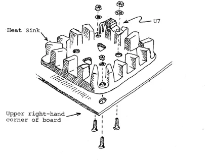
Step 1. Install heat sink. position the large, black heat sink (flat side to board) over the square foil area in the upper right corner. Orient the sink so that the two tri-angles of mounting holes in the board are under the two triangular cutouts in the sink. Using two 6-32 screws,
lockwashers and nuts, attach heat sink to board. Insert the screws from back (solder) side of board. (See Figure 2-2.) Step 2. Install U7 (7805UC or LM340T-5.0). position u7 over left-hand cutout in heat sink and observe how the leads must be bent to fit the mounting holes. Note that the center lead (3) must be bent downwards at a point approximately 0.2 inches further from the body than the other two leads. Bend the leads so that no contact is made with the heat sink when U7 is flat against the sink and its mounting hole is aligned with the hole in the sink. Fasten U7 to sink using a 6-32
screw, lockwasher and nut. Insert screw from back (solder) side of .board. Solder and trim leads. (Refer to Figure 2-2.)
. Heat
Upper right-hand~ corner of board
@
I ~J • . ~
,~. c..--U7
[image:17.612.134.549.384.701.2]CUTS, COMPUTER USERS TAPE SYSTEM SECTION II
(W{
Step 3. Install male Molex right angle connectors in loca-tions Jl and J2. Position connector with longer pins facing the top of the board, insert leads in mounting holes and -solder.(v(
Step 4. Install diodes Dl, D2 and D4 (lN4148)l respective locations. position Dl and D2 with
band mark (cathode) at the top and position D4
in their their dark with its band
!
at the right. Solder and trim leads.(') step 5. Install diode D3 (lNS242) in its location. Posi-tion D3 with its dark band mark ,(cathode) at the right.
(~
(~
Step 6. Install transistors Ql, Q3 and Q4 (2N2222) in their respective locations. position Ql with its emitter lead
(closest to tab on can) at the top and its base lead at the left. Position both Q3 and Q4 with their emitter leads at the right and their base leads at the top. Insert leads and push straight down on transistor until i t is 3/16" above the surface of the board. Solder and trim leads.
Step 7. Install transistor Q2 (2N4360) in its location. position Q2 with its flat side at the bottom, insert leads and push straight down on transistor until i t is 3/16" above the surface of the board. Solder and trim leads.
(
~
Step 8. Install transistor QS (2N2907) in its location. Position QS with its emitter lead (closest to tab on can) at the right and its base lead at the top. Insert leads and push straight down on transistor until i t is 3/16" above thesurface of the board. Solder and trim leads.
(~
Step 9. Install all resistors in numerical order in the in-dicated locations. Bend leads to fit distance between mount-ing holes, insert leads, pull down snug to board, bend leads outward on solder (back) side of board, solder and trim.LOCATION VALUE (ohms) COLOR CODE
(~
Rl 100 K brown-black-yellow( , ) R2 10 K brown-black-orange
( )
R3 1.SK brown-green-red( )
R4 10 K brown-black-orangeC
RS 1.SK brown-green-red( R6 1.SK
"
"
"
( R7 10 K brown-black-orange
( R8 150 K brown-green-yellow
( . R9 10 K brown-black-orange
~~
RIO 1 M brown-black-greenRll 10 K brovm -black-orange
Step 9 continued. LOCATION
~d~ ~i~
( - R14 ( . R15 R16 R17 R18 R19 R20 ( .) R2l
j!m
(:,r
VRIVALUE ( ohms) 2.2M 10 K 150 K 10 K
470 100 100 K
K K
10 10 470
39,2 watt 100 K 100 K
1 M
50 K
COLOR -CODE red-red-green
brown-balck-orange brown-green-yellow brown-black-orange yellow-violet brown brown-black-brown brown-black-yellow brown-black-orange
II II II
yellow-violet-brown orange-white-black brown-black-yellow
II II II
brown-black-green Potentiometer
"A
Step 10. Install resistor networks RXI and RX2 (2.2K ohms) in their respective locations. Position RXI so that the dot on its package is at the right end. Position RX2 with its dot at the left end.CAUTION
THESE RESISTOR NETWORKS ARE DELICATE. HANDLE WITH CARE.
( ) Step 11. Install the five tantalum capacitors in the fol-lowing locations. Take care to observe proper values and the correct orientation.
,
LOCATION VALUE (ufd) ORIENTATION
l~
C7 15 11+11 lead leftC8 15 11+11 lead top left
~
·f
C21 1 11+11 lead topC24 15 11+11 lead right
(t%
C29 1 11+11 lead top( ) Step 12. Install the following capacitors in the indicated locations. Take care to observe the proper value and type for each installation. Bend leads outward on solder (back) side of board, solder and trim.
Continued on Page 11-12.
CUTS, COMPUTER USERS TAPE SYSTEM SECTION II
( JJ)
( ( ( , ( ' -
(
((
)
( Ii )( )
(
)
( (-( )
( . ) ( ) ( ( ( (' )(~)
( )
(
.)
( )
un
(If )(J
Step 12 continued.
Disc capacitor leads are usually coated with wax during the manufacturing pro-cess. After inserting leads through mounting holes, remove capacitor and clear the holes of any wax. Re-insert and install.
LOCATION VALUE (ufd)
Cl .1
C2 .1
C3 .1
C4 .01
C5 .1
C6 .1
C9 .1
CIO .1
Cll .001
C12 .1
C13 .1
C14 .001
C15 .1
C16 .1
C17 .1
C18 .1
C19 .1
C20 .001
C22 .001
C23 .1
C25 .001
C26 .1
C27 .1
C28 .1
C30 .1
C31 470 pfd
Disc II II
Mylar tubular Disc
Mylar tubular Disc
II II II II
Step 13. Install Augat pins in mounting holes A, Band C. (These three holes are located to the left of U16, just below the lower mounting hole for R17.)
NOTE
You will find i t helpful to hold the board between two objects so that i t
stands on edge.
Step 13 continued.
To install an Augat pin, insert i t into the mounting hole from the component (front) side of board and solder the pin from the solder (back) side of the board so the solder
"wicks up" to the front side. (This will hold the pin firm-ly in place.)
Then insert a component lead into the pin and reheat the solder. Using the component lead, adjust pin until i t is perpendicular to board. Allow solder to cool while holding
the pin as steady as possible.
If the cooled solder is mottled or crystallized, a "cold joint" is indi-cated, and the solder should be reheated. Step 14.
switch so tion, the the first
Install DIP switch in location Sl. Switch No. 1 is at the left. (With ON position of each switch is ~.)
seven switches are active.
position this orienta-Note that only
(~step
15. Install DIP reed relays in locations Kl and K2.Be sure to position each relay with its end notch at the top (pin 1 in upper left corner). These relays are soldered to Ihe board. (Refer to "Loading DIP Devices" in Appendix IV.)
(0{
Step 16. Install U6 (1458 or 5558) in its location. Posi-U6 with its end notch at the top (pin 1 in upper leftcorner) and solder to board. (Refer to "Loading DIP Devices" in Appendix IV.)
(~step
17. Install U5 (78L12) in its location just above U6. position u5 with its flat side at the bottom, insert leads and push straight down until i t is 3/16" above the surface of the board. Solder and trim leads.~~tep
18. Install DIP sockets. Install each socket in theindicated location with its end notch oriented as shown on the circuit board and assembly drawing. Take care-not to-create solder bridges between the pins and/or traces.
INSTALLATION TIP
Insert socket pins into mounting pads of appropriate location. On back (solder) side of board, bend pins at opposite cor-ners of socket (e.g. pins 1 and 9 on a Continued on Page 11-14.
CUTS, COMPUTER USERS TAPE SYSTEM . SECTION II
Step 18 continued.
l6-pin socket) outward until they are at a 450 angle to the board surface. This
secures the socket until i t is soldered. Repeat this procedure with each socket until all are secured to the board. Solder the unbent pins on all sockets. Then straighten the bent pins to their original position and solder.
LOCATION TYPE SOCKET
Ul 14 pin
U2 16 pin
U3 14 pin
U4 14 pin
U8 16 pin
U9 16 pin
UIO 14 pin
Ull 16 pin
U12 16 pin
U13 16 pin
U14 14 pin
U15 14 pin
U16 16 pin
U17 16 pin
U18 40 pin
U19 14 pin
U20 16 pin
U2l 14 pin
U22 16 pin
U23 16 pin
U24 14 pin
U25 14 pin
( J
SteE 19.USin~2:24
bare wire,i::t:~:
jumpers according1
your selection of the options described in Section III. ( ) Step~Q. Set DIP switches (Sl) to select port address asdescribed in Section III.
All Processor Technology software is writ-ten with a CUTS port of FA (hex). To set the DIP switches for port FA, place Switch No. 2 in OFF position and the remaining
switches in the ON position.
(~step
21. Check operation of the regulators. This check is made to prevent potential damage to the IC's from incorrect voltages.( :../ Using an ohmmeter, make the following measurements:
SUPPLY MEASUREMENT POINTS
+ 5 V dc Ground to right-hand lead of U7 Ground to left-hand lead of U7 +12
-12
V dc Ground to positive (+) lead of C8 Ground to Pin 8 of U6 socket
V dc Across C21
You should measure some resistance in all three measure-ments. Zero resistance indicates a short. If required, find and correct the problem before proceeding.
J
( ) Install CUTS in computer. (The use of a Processor Tech-nology EXB Extender Board is recommended.)
CAUTION
NEVER INSTALL OR REMOVE CIRCUIT BOARD WITH POWER ON.
Turn power on and make the following voltage measure-ments:
MEASUREMENT POINTS VOLTAGE (±S%)
Ground to Pin 1 of U18 Socket
+
5 V dc Ground to Pin 8 of U6 Socket +12 V dc . Ground to Pin 2 of U18 Socket -12 V dcIf any voltage is incorrect, determine and correct the cause before proceeding.
If voltages are correct, turn power off, remove CUTS from computer and go on to Step 22.
Step 22. Install the following IC's in the indicated loca-tions. Pay careful attention to the proper orientation. Continued on Page II-16.
CUTS, COMPUTER USERS TAPE SYSTEM SECTION II
( )
Step 22 Continued.
Ste12
Pin 1 is positioned at the upper left cor-ner of each IC location, and is indicated by a dot on the PC board and assembly drawing.
IC NO. TYPE
~~
Ul* 4023*U2* 4027*
( - U3* 4013*
(
.
U4* 4013*( U8* 4520*
( u9* 4019*
(
.
UIO* 4024*( Ull* 4046*
( U12 74LS163
( , U13 74LS175
( U14 74LS136
( U15 74LS136
(
)
. U16 74LS367(i
U17 74LS367( . U18* 6011*
~~)
u19* 4030*!~
U20 74LSI09U21 74LS132
U2'2* 4049*
U23 74LS155
( ) U24 74LS04
..
~j
U25 74LS08U26 74LS08
*MOS device. Refer to CAUTION on Page II-7. 23. Adjust VRI.
If you do not have a voltmeter, set arrow on VRI to the "10 o'clock" position (as viewed from front side of board when VRI is at the top) and go on to Step 24. (In nearly all cases CUTS operates with VRI at 10 0 I clock. )
Step 23 continued.
(~
If you selected either the digital ormicrophon~
audiooutput options in Step 19, remove the jumper and install a jumper between Augat pins A and B.
(~If
you selected the auxiliary option in Step 19, leave tpe jumper between Augat pins A and B installed.(~onnect
pin 2 of Jl (IN) to pin 4 of Jl (OUT).( Install CUTS in computer and turn power on.
Set VRI fully clockwise (CW).
"
,-,,,
) Measure the DC voltage at pin ~of ~ and write the
mea-sured voltage down. (Call this Voltage A.)
Set VRI fully counterclockwiseG(CCW).
-, t(
I,
( Measure the DC voltage at pin ~of JiJ"r and write the
mea-sured voltage down. (Call this Voltage B.)
Add Voltages A and B and divide the sum by 2. (Call the
result Voltage C.) An example follows:
Voltage A (VRI fully CW): 3.45 V dc
Voltage B (VRI fully CCW): 1.80 V dc
A + B
=
5.25 V dcVoltage C
=
5.25 V dc/2=
2.63 V dc( ) Adjust VR 1 so that the voltage at pin 3 of U2 equals
Voltage C. (In the preceding example this would be
2.63 V dc.)
Step 24. Disconnect pin 2 of Jl from pin 4 of Jl.
( ) Step 25. If required by your option selection, remove the
A-to-B jumper- and re-install the A-to-D or A-to-C jumper as
appropriate. Otherwise, leave the A-to-B jumper in and go
on to Step 26.
( ) Step 26. Using the two female mating connectors supplied
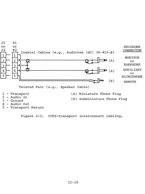
for Jl and J2, fabricate one or two, as required by your needs, CUTS-to-Recorder interconnect cables as shown in
Figure 2-3 on Page 11-18.
CUTS, COMPUTER USERS TAPE SYSTEM
Jl PI or
J2
or P2
Coaxial Cables (e.g., Audiotex (GC)
Twisted Pair (e.g., Speaker Cable)
30-415-5) (A)
(A)
(B)
SECTION II
RECORDER CONNECTOR
MONITOR or EARPHONE AUXILIARY
or MICROPHONE
REMOTE
1 - Transport 2 - Audio In 3 - Ground
(A) Miniature Phone Plug (B) Subminiature Phone Plug 4 - Audio Out
5 - Transport Return
[image:26.612.46.548.103.776.2]CUTS, COMPUTER USERS TAPE SYSTEM
Processor
Technology
Processor Technology Corporation
CUTS, COMPUTER USERS TAPE SYSTEM SECTION III
3.1 OPTION SELECTION
Jumper options that control two operating parameters, data rate and audio output, are provided on the CUTS Module. The port address for the module is selectable with seven switches. Use the following selection instructions along with the assembly drawing in Section VI.
3.2 PORT ADDRESS SELECTION (DIP Switch, Sl)
One of 130 possible port addresses, from
¢
through FA (hex), 254 (decimal), for the CUTS is selectable with the first seven DIP switch positions in location Sl.All Processor Technoloqy software is written for a CUTS port assignment of FA (hex). To configure your CUTS for this port, set Switch No.2 (Sl-2) to OFF and Switch NO's. 1 (Sl-l) and 3 through 7
(Sl-3 through Sl-7) to ON.
To select another port, set Sl-l through Sl-7 as required for the desired address. with these switches the address increases from ¢ (all seven switches open) in a binary fashion to 254, decimal,
(all seven switches closed). When setting these switches, keep in m~nd that 1) Sl-7 and Sl-l are the most and least significant bits respectively and 2) a closed switch is equivalent to a binary 1.
3.3 AUDIO OUTPUT SELECTION
The A, B, C, D jumper arrangement (to the left of U16) de-termines the audio output signal supplied to Jl and J2. Three choices are available: 1) a 5 V peak-to-peak signal for driving digital recorders, 2) a 250 mV signal for driving the auxiliary in-put to an audio cassette recorder, and 3) a 50 mV signal for driving the microphone input to an audio cassette recorder.
For audio cassette recorders, the auxi-liary input is preferred and recommended over the microphone input.
To select the digital recorder output, install a jumper (#24 bare wire is recommended~ between Augat pin A and the mounting pad labeled D.
To select the microphone output to drive the microphone in-put to an audio cassette recorder, install a jumper (#24 bare wire
is recommended) between Augat pins A and C.
3.4 DATA RATE SELECTION
Your CUTS is presently wired for both 1200 and 300 Baud operation, with the selection being program controlled. CUTS is designed, however, for operating at data rates up to 9600 Baud. The pad labeled AA, K, L, Q, R, S, T, U, V, W, X, Y and Z are provided for increasing the data rate. How the board is configured for higher rates will be the subject of a future addendum to this manual.
At this point in time Processor Technology does not recom-mend operation higher than 1200 Baud.
OPERATING PROCEDURES
CUTS, COMPUTER USERS TAPE SYSTEM
Processor
Technology
Processor Technology
Corporation
6200 Hollis Street
4.1 TAPE RECORDER
Any standard cassette tape recorder can be used with CUTS providing i t has the following features:
useful:
• ALC (automatic level control) in record mode • II Remote II on-off control input jack
• IIMonitor ll or lIearphone ll output jack
Though not required, the following recorder features will be
• Tone control
e Tape counter
@ IICue ll , IIPause ll or IIInstant Stopll control
Processor Technology currently uses the Panasonic Model RQ-413S with con-sistently good results.
4.2 CUTS-RECORDER INTERCONNECT (Single Recorder)
Using the interconnect cabling you fabricated in Step 26 of the IIAssembly-Test Procedure ll (Section II), make the following con-nections: (Refer to Figure 4-1 on Page IV-3. You may use either output connector Jl or J2 on the CUTS.)
1. Plug transport cable (Pins land 5 of Jl or J2) to re-mote jack on recorder.
2. Connect lIaudio out ll cable (Pin 4 of Jl or J2) to micro-phone or auxiliary jack on recorder, with the choice de-pending on the audio output selection you made. (Refer
to Paragraph 3.3'in Section III.) The auxiliary input is preferred and recommended over the microphone input. 3. Connect lIaudio inll cable (Pin 2 of Jl or J2) to monitor
or earphone jack on recorder.
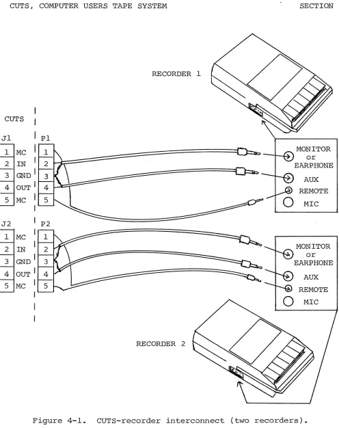
4.3 CUTS-RECORDER INTERCONNECT (Two Recorders)
Two recorders, under program control, can be driven by CUTS. In this case you will need two sets of the interconnect cabling described in Step 26 of the II Assembly-Test Procedure '\ (Section II).
CUTS, COMPUTER USERS TAPE SYSTEM· SECTION IV
Using these interconnect cables, connect the CUTS and re-corders as shown in Figure 4-1.
When using two recorders you may read or write to both under program control as well as read one tape while writing on the other.
If you intend to read one tape while writing on the other, however, you may have to disconnect the "monitor" plug from the write unit, with the need for disconnect being determined by the recorder design. The monitor disconnect must be made if the re-corder provides a "monitor" output in the record mode. (Panasonic RQ-413S and RQ-309DS do, for example.)
4.4 4.4.1
NOTE 1
Recorders on which the "monitor" jack is labeled MONITOR usually provide a monitor output in the record mode. If the jack
is labeled EAR or EARPHONE, the recorder usually does not provide a monitor output in the record mode.
NOTE 2
To determine if your recorder provides a monitor output in the record mode, install a blank tape, plug earphone into "monitor"
jack and microphone into microphone jack, set recorder controls to record, and
speak into microphone while listening with the earphone. If you hear yourself through the earphone, your recorder does provide a monitor output in the record mode.
RECORDER ADJUSTMENTS Volume Control
Since CUTS cui try in the read the Volume Control write operations.
incorporates AGC (automatic gain control) cir-mode and the recorder has ALC in the record cir-mode,
setting should not be critical for either read or Simply set the control at midrange and forget i t . 4.4.2 Tone Control
RECORDER 1
CUTS
Jl PI
1 MC
or
2 IN EARPHONE
3 GND
I
AUX
4 OUT I REMOTE
5 MC
I
MICJ2 P2
1 MC 1
2 IN 2 MONITOR
GND I or
3 3 EARPHONE
4 OUT I 4 AUX
5 MC I 5 REMOTE
0
MICRECORDER 2
Figure 4-1. CUTS-recorder interconnect (two recorders).
[image:33.612.65.561.68.694.2]CUTS, COMPUTER USERS TAPE SYSTEM SECTION IV
4.5 WRITE OPERATIONS
Other than placing the recorder in the record mode, loading the tape and making sure that the head is on tape (not leader), no manual operations are needed to write on tape.
4.6 READ OPERATIONS
When reading tapes, you must start the tape at least two sec-onds ahead of the data block you want to read. (CUTS tapes have a standardized header before each data block.) This two second delay is needed to allow the recorder playback electronics and the CUTS circuitry to stabilize after power is turned on.
Use the following procedure for loading tapes:
1. Disconnect monitor and remote plugs from recorder. (On most recorders this must be done in order to listen to . the tape.)
2. Load prerecorded cassette and play tape until you hear data. (Data sounds like noise in CUTS format.)
Absence of data is indicated by a pure 1200 Hz or 2400 Hz tone if recorded at 1200 bps or 300 bps respectively in the Byte/Kansas City Standard format.
3. Rewind tape far enough so i t will take two seconds to reach the data block you want to read after the recorder is placed in the playback mode. STOP RECORDER AT THIS POINT.
4. Set Volume Control as specified in Paragraph 4.4.1 if necessary.
5. Reconnect monitor and remote plugs to recorder. 6. Place "play" control on recorder in play position.
CUTS, COMPUTER USERS TAPE SYSTEM
Processor
Technology
ProcessorTechnology Corporation
6200 Hollis Street
CUTS, COMPUTER USERS TAPE SYSTEM SECTION V
5.1 INTRODUCTION
The CUTS module functions to transfer data bidirectionally between a computer and one or two audio cassette recorders. To
per-form its function, the module contains circuitry related to: 1. port address recognition,
2. computer-CUTS buffering,
3. computer input/output command decoding, 4. timing,
5. status reporting,
6. recorder on/Off control,
7. parallel-to-serial and digital-to-audio conversions in the write mode,
8. audio-to-digital and serial-to-parallel conversions in 9. and conversion of read data to NRZ (non-return to zero)
format.
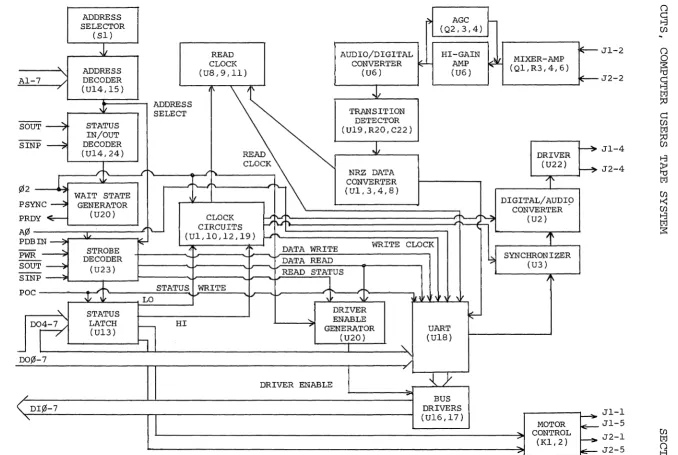
5.2 BLOCK DIAGRAM ANALYSIS
A simplified block diagram of the CUTS module is provided in Figure 5-1.
An address selector defines the port address for the CUTS module. It wor¥s with the address decoder to determine if the ad-dress on Al-7 matches the port adad-dress for the module. If i t does, the decoder produces the indicated CARD SELECT output to enable the status in/out and strobe decoders.
Once an input or output request from the processor is recog-nized, the status in/out decoder enables a PRDY line driver in the wait state generator. This generator inserts one wait state into every input or output request from the processor.
The strobe decoder decodes the indicated inputs from the processor to produce the STATUS WRITE, READ STATUS, DATA READ and DATA WRITE strobe signals.
been accepted. It also resets the driver enable generator to imme-diately enable the DI bus drivers.
If the cycle is an output cycle and A¢ is high, the strobe decoder outputs a DATA WRITE which transfers DO bus data into the UART and initiates serial transmission by the UART. Should A¢ be low, the strobe decoder outputs a STATUS WRITE. STATUS WRITE strobes the data on D04-7 into the status latch.
The four status bits in this latch are concerned with record-er motor control and data rate. One output turns one recorder motor on and off, another turns a second recorder motor on and off, a
third selects a low data rate, and the fourth selects a high data rate.
Timing for the CUTS module is supplied by the clock circuits and read clock. Clock circuitry manipulates ¢2 to supply WRITE
CLOCK as well as various other timing signals required to obtain two data rates. Read clock uses NRZ data transitions and one of two clock signals to generate READ CLOCK for use in the read mode.
When CUTS is in the write mode, parallel data on DO¢-7 is serialized in the UART and applied to a synchronizer in the NRZ for-mat. The synchronizer in turn establishes the time at which the bit cell from the UART starts. The digital-to-audio converter converts the data bit levels into corresponding audio signals. These signals are then fed through a driver to the audio output jacks.
In the read mode, inputs from the recorders are mixed and amplified, with an AGC circuit operating on the second stage. Fol-lowing amplification the audio signals are converted into digital signals, the transitions of which are detected and converted into the NRZ format. NRZ data is applied to the UART which performs the required serial-to-parallel conversion and supplies the parallel data to the DI bus drivers.
5.3 THEORY OF OPERATION
Refer to CUTS schematic in section VI. 5.3.1 Timing
All timing for the CUTS module is derived from, or related to, the 2 MHz ¢2 clock from the computer. As can be seen on the schematic, ¢2 is received on pin 24 of the S-IOO bus by a hysteresis receiver, U21. The inverted ¢2 directly clocks both sections of U20 as well as U12. One half of U20 (clock pin 12) serves as the wait state generator~ the other half generates the DRIVER ENABLE signal.
U12, preset to count 3, divides ¢2 by 13 to produce a 153.85 KHz signal on pin 11. The output of U12 is in turn counted down in
<:
I
W
AI-7
SOUT ----7
SINP ~
¢2
L
PSYNC ~
PRDY ~
A¢
PDBIN ---?
PWR --.:;;
SOUT ~
SINP~
POC
"-DO~
-00,0 7
/
( DI¢-7
"-SELECTOR (SI) ,~ ADDRESS DECODER (UI4,15) Ji STATUS IN/OUT DECODER (UI4,24)
+
WAIT STATE GENERATOR (U20) STROBE DECODER (U23)
~t
STATUS LATCH (UI3)r> (Q2,3,4)
READ AUDIO/DIGITAL HI-GAIN
CLOCK CONVERTER ~ AMP
(US,9,1l) (U6) (U6)
I' ~
ADDRESS
SELECT TRANSITION
DETECTOR (UI9,R20,C22)
READ
.1
CLOCK
;"~
"'"
NRZ DATAr - - ' ' - - I ' ...
"-
CONVERTER(Ul, 3,4, S)
,
CLOCK
~ ~
,,~ CIRCUITS
' ' - - - I
(Ul,10,12,19) i-J'h.
'\
~
4' ; i.--- DATA WRITE WRITE CLOCK
DATA READ
~
1..----.. READ STATUS
STATUS WRITE
1
-LO 'J' '>. In
'n
:,
,
\11DRIVER
~
HI 7 ' "- ENABLE ~GENERATOR UART
(U20)
,
(UlS)"
I
"DRIVER ENABLE { } '
BUS DRIVERS (UI6,17)
~
MIXER-AMP(Ql,R3,4,6) DRIVER (U22)
l'
DIGITAL/AUDI9 CONVERTER"? (U2)
l'
~ SYNCHRONIZER (U3)
J
MOTOR
" CONTROL
--::> (Kl,2) ~
...
IE---~ ~ ~ f----7IE-
r---- E--JI-2 J2-2 JI-4 J2-4 Jl-l JI-5 J2-1 J2-5 1-3 Cfl () 0:s:
'U~
I::Ij :;0 c::: Cfl I::Ij::0 'U
Cfl :;0
0
1-3 ()
~ I::Ij
'U Cfl
I::Ij Cfl
0
Cfl :;0
t-<:
Cfl 1-3 1-3 I::Ij I::Ij ()
:s:
ij
[image:38.792.57.735.78.533.2]UlO, a seven-stage binary counter, to provide 38.4 KHz on Q2, 19.2 KHz on Q3, 4800 Hz on Q5, 2400 Hz on Q6 and 1200 Hz on Q7. The
clocks on Q6 and Q7 are used in the write data synchronizer (U3) and and the digital-to-audio converter (U2).
The remaining outputs from UIO are fed to two sections of U9, a quad multiplexer or select gate. All four sections of U9 are used to select clocks for low speed or high speed operation according to the select inputs, pins 9 (a) and 14 (B). The states of these two select inputs must be complementary to each other in order to select the high or low speed clocks. Specifically, A must be high and B low to select high speed clocks: the converse condition selects low speed clocks. The select inputs are supplied by the complementary outputs of one section in U13, the status latch.
The output of the second section of U9 is WRITE CLOCK, 4800 Hz on low speed and 19.2 KHz on high speed. The third section out-puts a 19.2 KHz (high speed) or 38.4 KHz (low speed) timing signal
to U8 in the NRZ data conversion circuit.
READ CLOCK is produced by ull (a phase locked loop), U8 (a binary counter) and the remaining two sections in U9. The signal
input (pin 14) to ull is supplied from pin 1 of U3 in the NRZ data conversion circuit. It is a constant frequency, regardless of whe-ther one or two transitions are detected in the read data during the count out time (12 counts) of the counter (U8) in the NRZ conversion circuit. A phase comparator in Ull compares the signal input to the output of a voltage controlled oscillator (VCO) in Ull (pin 4). By feeding the VCO output through a counter (the other half of U8) be-fore feeding the counter output back to the compare input (pin 3) of Ull, the circuit acts as a frequency multiplier. The output of this circuit remains locked, therefore, to a multiple of the signal input on pin 14 of Ull.
The output of ull is nominally 19.2 KHz. Remember that the actual output is determined by the signal input which in turn is a function of tape speed. In other words, the phase lock loop circuit tracks input frequency variations. And i t will track such varia-tions within its locking range which is determined by the setting of VRI (connected to pin 12 of Ull).
On high speed, the divide by four output of U8 (pin 12) is selected as RECEIVE CLOCK. The VCO output of Ull is selected for the low speed RECEIVE CLOCK.
5.3.2 Control
Basically the wait state generator (~ of U20), address se-lector and decoder (Sl, u14 and U15), strobe decoder (U23), driver enable generator (~ of U20), the status latch (U13), the status in/ out decoder (U14 and 24), motor control (Kl and 2), and power on clear (U21) comprise the CUTS control circuitry.
CUTS, COMPUTER USERS TAPE SYSTEM SECTION V
The address selector and decoder consists of seven open col-lector exclusive-OR gates, the inputs of which are connected to Al-~ RXI and Sl. RXI and Sl function as the selector which is configured to reflect the complement of the module address. That is, a response to a high on an address line is generated by the applicable gate by grounding the other input by closing the appropriate DIP switch position. When the decoder senses an address match, all the gates
respond true and RX2-4 pulls the outputs up to a high level CARD SELECT signal.
CARD SELECT enables the output gate (U2l) in the status in/ out decoder. This gate is satisfied if, and only if, SOUT or SINP
is active to indicate either an input or output operation is under way. The output (pin 6) of U2l enables the PRDY line driver.
The input to this driver is provided on pin 10 of U20, the wait state generator which is clocked by ¢2 and reset by PSYNC.
Thus, pin 10 of U20 goes high on the falling edge of ¢2 after PSYNC. This is the time during which the processor tests for wait requests. The purpose of this half of U20, therefore, is to insert one wait state into every input or output request by the processor. This is required to lengthen the data strobes to durations required by the UART.
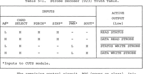
U23, the strobe decoder, decodes SINP, PDBIN, SOUT, PWR and A¢ to produce STATUS WRITE, READ STATUS, DATA READ STROBE, and DATA WRITE STROBE. The truth table for U23 is provided in Table S-l on Page V-6. All outputs from U23 are low active.
READ STATUS is applied to the J and K inputs to the other half of U20 which is clocked by ¢2. Thus, an active READ STATUS signal produces a DRIVER ENABLE which is delayed from the strobe by one-half a ¢2 cycle. This signal enables the tri-state buffers
(U16 and 17) to place data on the DI bus. Note that a DATA READ STROBE resets U20 to immediately enable the DI bus buffers.
Table 5-1., Strobe Decoder (U23) Truth Table.
INPUTS
ACTIVE
CARD - - OUTPUT
A¢* SELECT PDBIN* SINP* PWR* SOUT* (Low)
L H H H
-
-
READ STATUSH H H H
-
-
DATA READ STROBEL H
-
-
L H STATUS WRITE STROBEH H
-
-
L H DATA WRITE STROBE*Inputs to CUTS module.
The remaining control circuit, POC (power on clear), ini-tializes the CUTS whenever power is applied. When power is applied, POC on S-IOO bus pin 99 goes low. POC is inverted in one section of U21 to clear the logic in the UART (UlS). In addition, the inverted POC is again inverted in one section of U24 to clear the status re-gister, U13. This clear sets both motor control outputs as well as the high speed select bit high.
5.3.3 write Mode
When the CUTS is in the write mode, data is input to the UART (UlS) under control of the DATA WRITE STROBE signal from U23. Upon completion of this strobe, the transmit sequence is initiated within the UART, with the transmission rate being governed by WRITE CLOCK.
The transmission sequence begins with a start bit, a low (data zero) on the UART's TO output. It is followed by eight data bits and two stop bits, with the number of bits being fixed by the connections to pins 34 through 39 of UIS. This data stream is
called NRZ data (non-return to zero) because the data never returns to zero until the next bit cell.
NRZ data from UIS is applied to the D input of U3, aD-type flip-flop which is clocked at 1200 Hz. Consequently, the output on pin 13 of U3 follows the input data on pin 9 after the rising edge of the 1200 Hz clock. This output is connected to the reset (pin 12) of U2, so when the data out of the UART is high, the first section
in U2 is forced to a reset condition. In this condition the J and K inputs to the second stage of U2 are held high which allows the flip-flop to change state on the rising edge of the clock.
[image:41.612.43.535.101.356.2]CUTS, COMPUTER USERS TAPE SYSTEM SECTION V
The clock for U2 is 2400 Hz in the high speed mode or 4800 Hz in the low speed mode. This clock is derived from the 2400 Hz output of UIO in conjunction with the low speed select signal NAND gate Ul and exclusive-OR gate U19.
In the high speed mode, pins 4 and 5 of Ul are held low, thus holding pin 6 of Ul high. As a result the 2400 Hz signal is inverted in Ul19 to become the clock for U2.
Pins 4 and 5 of Ul are held high, however, in the low speed mode to enable Ul. In this case R19 and C20 provide a delay in the Ul gate. When the 2400 Hz signal on pin 9 of U19 changes state; so does pin 10 of U19. Also, C20 charges through R19 for several hun-dred nanoseconds, at which point pin 6 of Ul is brought to the op-posite polarity. The output from U19 then goes high. A series of positive pulses, with a pulse width approximately equal to the R19, C20 time constant and occuring at every transition of the 2400 Hz signal, appears on pin 10 of U19. This circuit thus operates as a frequency doubler in the low speed mode to provide a 4800 Hz clock for U2.
The 2400 Hz signal from which the U2 clocks are derived al-so produces the 1200 Hz clock signal for U3 by toggling the flip-flop in UIO. As a result the 1200 Hz signal changes state follow-ing a propagation delay after the 2400 Hz signal falls.
As previously stated, the second stage of U2 is allowed to change state on the positive going transitions of the U2 clock as long as the data out of the synchronizer is a 11111. The end result is an output on pin 2 of U2 that is one-half the clock frequency
(1200 Hz and 2400 Hz in the high and low speed modes respectively). Assume the data stream out of the UART goes low (110 11 ). On the next rising edge of the 1200 Hz signal, U3 will reset with Q
low and
Q
high. A low reset on pin 12 of U2 enables the first U2 stage to toggle on the next rising edge of the U2 clock which occurs 1/2400 second after the synchronizer output falls. Remember that the U2 clock moves from a lqw to a high shortly before the 1200 Hz signal did. The reset on pin 12 of U2 is thus removed slightly after the U2 clock occurred. with the J and K inputs to the first U2 stage high, its output will change state on each succeeding low to high transition of U2 clock. The second U2 stage in turn can only toggle on the positive going transition of U2 clock when itsJ and K inputs are high. Since the inputs are high at one-half the clock rate, by virtue of the first U2 stage, the second U2 stage toggles at one-fourth the clock rate.
1200 Hz represents a 11111 and one-half cycle of 600 Hz represents a
11011 •
The output on pin 2 of U2 is applied to one section in U22 which provides sU'fficient current drive for the R15, 16 and 17 divi-der network. This divider and a jumper arrangement allow selecting one of three outputs to be fed to the audio output jack *Jl-4 and J2-4}. The A-to-D jumper selects a 4-volt peak-to-peak square wave output for a digital recorder~ the A-to-B jumper selects a 270 mv
signal for the auxiliary input to an audio recorder~ the A-to-C jumper selects a 50 mv signal for th~ microphone input to an audio recorder.
5.3.4 Read Mode
When CUTS is in ters oh Jl-2 and J2-2. tive mixer (R3,4 and 6) put of which is applied amplifier U6.
the read mode, data from the recorders en-These two inputs are mixed through a resis-and fed to Ql, an emitter follower, the out-to the negative input (pin 2) of operational
The first section of U6 is a high gain amplifier, with its gain being determined by R9 and RIO. The output from this amplifier is coupled to the input (pin 6) of the following U6 stage and the base of a Darlington pair (Q3 and 4) which provides high current gain.
Current into the base of Q3 causes C29 to discharge. (C29 charges through R25 to 5 V dc.) The voltage on C29 in turn controls· the gate of FET (field effect transistor) Q2. Q2 functions as a
variable resistor which can be changed by its gate voltage. Since Q2 is connected between ground and the input network to the first U6
stage, i t serves as a variable shunt. A low gate voltage on Q2 decreases the shunt resistance and the input to u6. In a like man-ner, a high voltage on C29 results in an increased input to U6. Q2, 3 and 4 with their associated circuitry, therefore, serve as an AGC circuit which limits the input to the second U6 stage to approxi-mately a 2 vol.t peak signal.
The second stage of U6 performs the needed audio to digital conversion. Feedback resistor R12, in conjunction with R13, esta-blishes the level on the positive input (pin 5) of U6. This level, be i t positive or negative, is the threshold which the negative
input (pin 6) must exceed in order for the output of U6 to switch levels, positive to negative and the converse. Since the feedback loop is regenerative, U6 switches at its maximum rate, and u6
switches on each transition of the audio signal input. It is in this manner that U6 performs the audio to digital conversion.
The digital output of U6 is inverted in one section of U22 and applied to pin 2 of U19, an exclusive-OR gate which is connected as a buffer without inversion. If the output of U22 is low, the
CUTS, COMPUTER USERS TAPE SYSTEM SECTION V
output on pin 3 of u19 is also low and the output on pin 11 of u19 is high. The voltage across C22 under this condition is minimal. When the output of U22 goes high, C22 starts to charge through R20 until pin 2 of U19 crosses the threshold of that gate. At this point pin 3 of U19 goes high, and since the two inputs to the se-cond exclusive-OR gate are both high, pin 11 of U19 goes low. C22 now discharges because pins 2 and 3 of U19 are at the same level so that the circuit can repeat the operation on the next high to low transition at pin 4 of U22. R20, C22 and U19 consequently serve as a transition detector that produces a pulse less than one microsecond long for each transition of the output on pin 4 of U22,
regardless of the polarity of the transition.
Transition pulses from U19 clock ~ of U3 and ~ of U4, both of which are D-type flip-flops. A transition pulse clocks U3 to set
Q high and Q low to enable a binary counter, US. The Q output of U3 is applied to pin 5 of U4 and the circuit remains in this state until one of two things occurs: 1) a second transition pulse ar-rives before US reaches count 12 or 2) uS reaches count 12.
If a second transition pulse arrives before count 12, the first U4 stage is set and presents a 11111 to pin 9 of U4. - This is clocked by the -reset of U3 as a low to pin 12 of U4.
If a transition pulse does not arrive before count 12, the first U4 stage presents a 110" to pin 9 of U4. On count 12, the C and D outputs of US go high to reset U3 through Ul. As a result the U4 second stage clock goes high, as does pin 12 of U4. The output on pin 12 of U4, in the NRZ format, is inverted by U22 and applied to the receive input of the UART.
The Q output of U3, which occurs at the actual bit rate of the incoming data, is also used by the receive clock circuitry to reconstruct the receive clock from the data signal.
Received data undergoes serial-to-parallel conversion in the UART and placed on the ROl-S data outputs of the UART WHEN ROD
(pin 4 of the UART) is low. The received data is then gated through u16 and 17 to the DI bus.
Four status outputs from the UART can also be enabled when SFD (pin 16) is low. These four bits are FE (framing error), OE
CUTS, COMPUTER USERS TAPE SYSTEM
Processor
Technology
Processor Technology Corporation 6200 Hollis Street
COMPONENT Wf~ING
+8 + 8
-m
w
..J
w:
+
r
..:.(n=
+"18 "IS
-
X~Oy---v i a EXT CL~
VI1 ~TC
VI2 STSTS V!3 0lG1
VI4 FROY ViS VIS VI7
-X~OY2
-C/C OSSPS -UNPROC - P R O C - - 2 0 - 7 0 SS R U N AOO OSS P R O Y -0 -0 OSS P!NT
-;rJ 2 CLK PHOLO
-;rJ 1 CLI<;'" - - 2 5 - 7 5 PHLOA PSYNC
-PW~IT--PW~
-PINTE---POSH~
-AS Aa A 4 A1 A3 A2 A15 AS A12 A 7 AS A8
0 0 1 - - - A 1 3 - - - 3 5 - 8 5 0 0 0 A 1 4 -A10 "A ' 1 1
0 0 4 0 0 2 0 0 S O O 3 -0 -0 8 - - - -0 -0 7 - -40-90 01 2 - - - - 0 1 4 01 3 0 1 S 01 7 0 1 , 8 -SMI 01 1 -S O U T - - - O l a - - 4-S--S-S SINP SINTA , S M E I " ! SWO S H L T A S S T A C K -GNO G N O - - 50-100
t
ru 'l:J
. 0
-"
-IU 2
m -i
F"
m
~
----..."...'.-.yy~~I
- - - ,
1:"
-"
o o
<
-DATA
VI-2
JI AUDIO IN
JZ AUDIO IN
F'''' (0
Z 1---_""I.SI\Kr---,/
"'"
10K
JI TAP~ T~AN.sP"'~'Tl
, 31 ~AP" TI<'AN:50I"'OI<Tl Re:TU~N
Jt. TAP. TII'AN"POF<T;z. I
Cit.
ZN4~"'O
JZ TAPE TI<'AN~F"OF<T;z. R:&:TUI<'N ~~---~
,:~
tJ~ A PL-L-P'1"1P'a!C'/~"UNTi.1I: ~i50U8
'-"'''"
~""
~4;;'.zO 15
®
1L---~'Zz (~~~y)
NOHS:
I. - D I" I/O "'ONN~'::~"I<
1.. ----CJ I~ s.-Ie''' G't'NNi£':::1'IO,,",
~. D-- ," $-100 ""NNI!'::TION
DJ: ¢
.... I~V
-I~V
SCHE:MATIC:,5-IOO CUTS
1
-DRAWN n I,.I"'D ~ MA~~U . - , .... .::.'-8-77
DAn, q-:z.1-7~(,~L_~...:. _ _ ...:"_~_n ____ ...l_ •• _ _ _ ~ _ _'_
PROC:5SS0R TSCHNOl-06:Y
13 1 1
GJ
1 1 1 0 0 1 1 UART (NRZ Data)12 DATA WRITE STROBE
14 f ' )
J1J1JWUl
2400 Hz1 1 1 1 NRZ DATA (Synchronized to 1200 Hz Clock)
15
16
17 MANCHESTER ENCODED DATA
18 FILTERED MANCHESTER ENCODED DATA
NOTE: 1200 Baud NRZ data (13) is not necessarily synchronized with 1200 Hz
clock. Signal at 15 and its complement on pin 12 of U3 are.
1
2
3
4
5
6
7
8
9
10
11
CUTS
AUDIO IN (0.5 to 8 V p-p)
FILTERED AUDIO
(Approximately 2 V p-p)
DC level between 0.5 and 5 V dc depending in input signal
amplitude. DC level varies inversely with input amplitude.
-."j
I+-
Approximately 500 nsec---~f
'r'---
~
o V (Approximately
20 V p-p)
MANCHESTER ENCODED DATA (CMOS Level)
to Negative Edge
(Approximately 1200 Hz)
RECOVERED NRZ DATA
II 8080 Operating Codes III Standard Color Code
IV Loading DIP Devices, Soldering Tips and Installing Augat Pins V IC Pin Configurations
Processor
Technology
Processor
Technology Corporation
CUTS, COMPUTER USERS TAPE SYSTEM APPENDIX I
PROCESSOR TECHNOLOGY CORPORATION, in recognition of its
responsibility to provide quality components and adequate instruction for their proper assembly, warrants its products as follows:
All components sold by Processor Technology Corporation are purchased through normal factory distribution and any part which fails because of defects in workmanship or material will be replaced at no charge for a period of 3 months for kits, and one year for assembled modules, following the date of purchase. The defective part must be returned postpaid to Processor Technology Corporation within the warranty period.
Any malfunctioning module, purchased as a kit directly from Processor
Technology and returned to the factory within the three-month warranty per