Photonic crystal interfaces:
A design-driven approach
A thesis presented by
Melanie Ayre MEng.
to the
University of St Andrews
in application for the degree of
Doctor of Philosophy
Abstract
Photonic Crystal structures have been heralded as a disruptive technology for the miniaturization of opto-electronic devices, offering as they do the possibility of guiding and manipulating light in sub-micron scale waveguides. Applications of photonic crystal guiding - the ability to send light around sharp bends or compactly split signals into two or more channels have attracted a great deal of attention. Other effects of this waveguiding mechanism have become apparent, and attracted much interest - the novel dispersion surfaces of photonic crystal structures allow the possibility of “slow light” in a dielectric medium, which as well as the possibility of compact optical delay lines may allow enhanced light-matter interaction, and hence miniaturisation of active optical devices. I also consider a third, more traditional type of photonic crystal, in the form of a grating for surface coupling.
In this thesis, I address many of the aspects of passive photonic crystals, from the underlying theory through applied device modelling, fabrication concerns and experimental results and analysis. Further, for the devices studied, I consider both the relative merits of the photonic crystal approach and of my work compared to that of others in the field. Thus, the complete spectrum of photonic crystal devices is covered.
With regard to specific results, the highlights of the work contained in this thesis are as follows:
• Realisation of surface grating couplers in a novel material system demonstrating some of the highest reported fibre coupling efficiencies.
• Optimisation and experimental validation of photonic crystal routing elements (Y-splitter and bend).
Declaration
I, Melanie Ayre, hereby certify that this thesis, which is approximately 40,000 words in length, has been written by me, that is the record of work carried out by me, and that it has not been submitted in any previous application for a higher degree.
date signature of candidate
I was admitted as a research student in September 2002 and as a candidate for the degree of Ph.D. in September 2003; the higher study for which this is a record was carried out in the University of St.Andrews between 2002 and 2006.
date signature of candidate
I hereby certify that the candidate has fulfilled the conditions of the Resolution and Regulations appropriate for the degree of Ph.D. in the University of St. Andrews and that the candidate is qualified to submit this thesis in application for that degree.
Copyright
In submitting this thesis to the University of St Andrews I understand that I am giving permission for it to be made available for use in accordance with the regulations of the University Library for the time being in force, subject to any copyright vested in the work not being affected thereby. I also understand that the title and abstract will be published, and that a copy of the work may be made and supplied to any bona fide library or research worker.
Acknowledgments
In August 2002, as an exciting beginning to my doctoral studies, I was given the opportunity to travel to the town of Ascona, on the banks of Lago Maggiore in Switzerland, to attend a summer school on two dimensional photonic crystals. Having little experience of any kind of optics, I remember being alternatively amazed and baffled by the other delegates, the apparent breadth and depth of their knowledge, and their willingness to engage in vigorous debate with their elders and betters. I am particularly indebted to Maria Kotlyar, then a fellow St Andrews student, who helped me to hide my nervousness and inexperience! Arriving finally in St Andrews, I found myself part of a big research group under a mostly absent professor. Thankfully, with so many people around, I was well placed to start learning my new subject. I’d like to thank Rab Wilson, my post-doc, for helping me to see just how much I’d need to know about, if not actually know, and Mikey Settle and Steve Neale, who started their PhDs with me, just for being themselves. Donald Brown and Simon McGreehin helped me to see the importance of attention to detail, and Will Whelan-Curtin the importance of blind leaps of faith! There are now 35 current and former members of Prof. Krauss’s Microphotonics Group, and if they’d all been chosen solely to help me towards gaining my PhD they couldn’t have been better.
with a hard act to follow.
As for the elusive Prof. Krauss, well, I’m not sure I could’ve chosen a better PhD supervisor than Thomas. Since he’s so hard to get hold of, on technical matters I found myself asking the real experts for help first. This has meant that when I’ve finally managed to catch him, my opinion is well enough informed that I can be like one of those obstreperous delegates myself, trying to find the line between useful debate and pointless argument, and walk that knife edge carefully. For me, this has helped to maximise the benefits of having a well-known and travelled supervisor, always jetting off but returning full of enthusiasm, with new ideas and approaches to try. Although sometimes it’s been exhausting. So let me admit here what may not have been clear at the time - Thomas, at least sometimes, I really thought you were right!
On a personal note, I’d like to thank everyone who’s put up with me while I’ve been writing, especially Paul Cruickshank and Dave Bolton, both for constantly reminding me why it’s good to do a PhD, and making it easier; Elaine, Matt and John, who can always make time to watch a movie; Ruth and Christina for endless cups of tea; and my parents and grandparents, who’ve been desperately waiting for me to stop being a student.
Contents
Abstract ii
Declaration iv
Copyright v
Acknowledgments vi
1 Introduction 1
1.1 The role of PhCs . . . 1
1.2 Thesis structure . . . 3
2 Theory and modelling of photonic crystals 6 2.1 Introduction to photonic crystals . . . 6
2.2 Maxwell’s equations . . . 14
2.3 Practical numerical modelling of photonic crystal slabs . . . 15
2.4 Conclusion . . . 31
3 PhC fabrication techniques 33 3.1 Introduction . . . 33
3.2 Substrate choice . . . 34
3.4 Lithography . . . 37
3.5 Pattern transfer and etching . . . 47
3.6 Additional processes . . . 52
3.7 Conclusion . . . 52
4 Coupling into microphotonic devices 54 4.1 The coupling problem . . . 54
4.2 Fibre couplers . . . 56
4.3 Surface grating couplers . . . 58
4.4 Fabrication considerations . . . 71
4.5 Characterisation and testing . . . 82
4.6 Conclusions . . . 87
5 Photonic crystals and coupling 89 5.1 Optimisation of short tapers . . . 90
5.2 Photonic crystal interfaces . . . 101
5.3 Other studies - PhCs with elliptical holes for AWG design. . . . 111
6 PhC routing devices 124 6.1 Integrated optics and routing . . . 125
6.2 Design of integrated PhC coupler, Y-splitter and bend . . . 129
6.3 Device fabrication . . . 150
6.4 Measurement setup . . . 152
6.5 Principles of measurement analysis . . . 153
6.6 Results and analysis . . . 159
7 Conclusions 171
Chapter 1
Introduction
In this work, I will present the results of my research into Photonic Crystal (PhC) devices, undertaken in Prof. T.F. Krauss’ Microphotonics and Photonic Crystals Group at the University of St Andrews. In this introductory chapter, I will briefly explain the potential role of Photonic Crystal devices, and then outline the rest of this thesis - as I have studied a number of significantly different devices, the literature reviews are presented in their relevant context.
1.1
The role of PhCs
and designed to operate with fibre optic systems. A single functional device may have a length of several centimetres, which is unthinkable to electronics system designers! There are also high density optical technologies, with a feature size of the order of 1µm, which are more suited to integrate with ICs, and this integration is an active area of research.
For many years it has been recognised that optical communications and electronic data-processing technologies must converge. The ICs are increasingly limited by communications both on and between chips, and the demand for broadband internet is fueling an expansion in communications markets, albeit without the headlines of a few years ago. This convergence has proved rather more difficult than was hoped, with optical systems repeatedly proving more demanding than improved electronics, but the major players in the silicon industry still believe that optics will ultimately be necessary to the continued growth of the IC markets and technologies[1]. There is much still to do to enable effective use of optics technologies in ICs - a lingering issue being that modern high density integrated optics do not exist on silicon. Instead, indium phosphide and gallium arsenide are the choice semiconductors where active functionality is required, and silica-on-silicon, which is convenient for use with optical fibre, is prefered for passive systems. Although the search for silicon-based alternatives continues, the current thinking is to integrate suitable optics materials into the silicon platform where required.
dispersion properties of PhC devices are a strong contender for enhancing light-matter interactions [2, 3], thereby further reducing the device footprint. Particularly, I have studied the principles and techniques that can be used to design a range of photonic crystal devices, taking into account the practical matters of fabricating and characterising physical devices. I present a complete solution, taking light from a fibre into a semiconductor waveguide, then down to the small scale of PhCs, and finally coupling into a PhC device and using it for routing of light.
1.2
Thesis structure
In chapter 2, I discuss the background needed to understand the operation of PhC devices and their underlying theory, with a particular regard to justifying the choices that have been made for the designs presented in later chapters. Thereafter, we concern ourselves with devices and introduce the design techniques used, and both their strengths and weaknesses. As I have focussed on practical devices, it is necessary to actually fabricate them, to gain an understanding of the constraints that this implies. Hence, in chapter 3, I will discuss the fabrication technologies that have been used, concentrating particularly on the techniques that have been developed for effective PhC device fabrication here at St Andrews. In some ways my fabrication work is unusual, because for this thesis I have studied and made devices in the three major optics material systems: InP, SOI and AlGaAs. Each of these has their application in optics technologies, and also presents its own fabrication challenges. Many techniques only work for specific systems, as is explained in chapter 3.
been studied, beginning in chapter 4 with a surface grating coupler on InP that very successfully couples light from an optical fibre on to a chip. The principles behind the design are elaborated, before concentrating on the specific fabrication effort to realise these devices. Finally measurement results are presented. This work has been undertaken in collaboration with Universiteit Gent, in Belgium.
These couplers are relatively large devices, dictated by the 6µm mode diameter of standard single mode fibre. This means that the coupler itself has a footprint of around 12µm2
. PhC devices at telecommunications wavelengths have a mode diameter of around 500nm. A standard adiabatic taper between these two scales is over 500µm in length. This represents the major part of the device footprint in many cases, and hence is undesirable. In chapter 5, we use multimode interference techniques to try and reduce this length, successfully designing and characterising a taper which is only 9µm long. I also present some work which has been undertaken to try and improve the coupling into a PhC, making use of impedance matching techniques, and suggest a design which appears to work in theory. I also discuss a Mach-Zehnder Inteferometer device design which was carefully studied in terms of coupling, which would require a successful interface design to couple light efficiently and without reflection or loss, and hence show effective use of the anomalous dispersion of PhCs.
reproduction of the design. This was carried out in collaboration with Photon Design, an electromagnetics software company based in Oxford, UK.
Chapter 2
Theory and modelling of
photonic crystals
In this chapter, I will introduce Photonic Crystals (PhCs) in a conceptual way, explaining the origins of the effects that I will refer to continually in chapters 4, 5, and 6. I will then introduce the modelling techniques used to study the devices presented in these chapters. Both time domain and frequency domain techniques have been used, and will be compared. In general, time domain methods are simpler to understand and use, but frequency domain techniques can be more powerful, and give greater insight into problems. The key with both methods is to determine a dispersion diagram which agrees with a transmission model.
2.1
Introduction to photonic crystals
Maxwell’s equations to gain this data, and so it seems more appropriate to start with the concepts I work with. However, to use such programs effectively it is necessary to understand the mathematics and algorithms behind them, so I will return to Maxwell shortly.
We start with a PhC as a periodically patterned dielectric, for example a Bragg stack in a 1D system, or opals in 3D. The key discovery was made independently by Yablonovitch and John, who both showed that a periodicity in all of the dimensions of a given space gives rise to an omnidirectional bandgap, because no states exist for propagation in any direction, for certain wavelengths. Further, they showed that the periodicity must be on the order of the wavelength for this bandgap to exist [4, 5, 6, 7, 8]. To do this, it was necessary to find periodic solutions to Maxwell’s equations, invoking the Floquet-Bloch theorum and many concepts from solid-state theory, particularly those of Brillouin Zones and Bloch Modes.
In saying that there are wavelengths where no states exist in PhC structures, we imply that there are wavelengths where states do exist. As these are the solutions to Maxwell’s equations, they necessarily define the propagating waveguide modes of the system - we commonly refer to these as lattice modes. They have been found to have interesting dispersion surfaces, and as a result the use of these lattices has been proposed and demonstrated for such devices as super-prisms and super-collimators [9, 10, 11].
concept of PhC slabs was developed by Joannopoulos [4] - using PhC effects in the plane, but waveguiding via total internal reflection (TIR) reflection in the third dimension. Although still challenging, as will be demonstrated in chapter 3, fabricating devices in planar PhCs is much simpler than in 3D crystals, as techniques developed for planar processing of conventional semiconductor devices can be adapted for this purpose. Hereafter, any reference to PhCs will strictly mean PhC slabs.
Planar PhCs inherit many properties from the slab waveguides they inhabit, and so strictly they should be modelled as complete 3D devices. However, because it is possible to separate these effects, the majority of the modelling work both in this thesis and in the PhC community is performed in 2D only, assuming that the third dimension is either infinite and uniform, or of zero size. Any simulations performed in 3D will have this noted. Of course, it is necessary to compare the results of 2D and 3D models, especially when assessing fabricated devices. For many structures the only major difference is a slight shift in frequency of spectral features.
To permit comparison between 2D models and real devices, we must have methods to determine the effects of the third dimension. Most importantly, we work with the concept of the lightline, which is superimposed on the dispersion diagrams that are calculated as ω =ck0, or u =k/ncladding in the normalised
units typically used. As even a PhC mode cannot be expected to propagate faster than light, states above this line on the dispersion diagram are inherently lossy - that is, they are quasi-guided or radiation modes.
and cladding (LOP), or like a photonic wire, with high ∆n(HOP). LOP devices are essential when one aims to integrate with active functionality. In this case, all operation must be above the lightline, but it is hoped that sufficient gain can be applied to overcome intrinsic losses. HOP devices, which can operate below the lightline, are much more suitable for waveguiding applications.
2.1.1
Photonic Crystal Slabs
For all PhC devices, the first point of reference is the bandstructure. In the next sections, I will describe ways in which these can be calculated, but here I will simply present the results, for 2D bandstructures. With PhC slabs, the first decision is whether to use a lattice of high index rods in a low index medium, or low index rods (i.e. holes) in a high index medium. It is the properties of rod systems that first caused excitement about PhC devices, as these have a wave guided in air; however these structures have no TIR confinement and so very long rods are needed. These are again very challenging to fabricate, and simpler fabrication is one of the motivations for slab PhCs. Hence, here I will exclusively study the properties of lattice-of-holes PhCs.
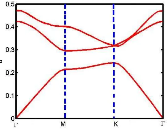
The next question is, what kind of lattice to use? It has been shown that triangular lattices have broader bandgaps than square lattices, essentially due to increased symmetry[13]. Hence we choose this system for most of the studies here. The exception is for the work on 2D grating couplers discussed in chapter 4 where it is essential that the basis vectors for a unit cell are orthogonal, and hence we use a square lattice. Figure 2.1 shows a typical bandstructure for a triangular lattice of holes1
.
1
Specifically, air holes through a material of refractive index 2.89, which is the effective
index value for the SOI slab used in later chapters, with a normalised hole radius of 0.28.
Figure 2.1: A typical dispersion diagram or bandstructure for a triangular lattice
of holes-type photonic crystal. The ordinate traces the edge of the irreducible
Brillouin zone for this structure. Γ, K and M are the vertices of the IBZ,
following standard symmetry labelling. This is the normalised k vector. The
abscissa is normalised frequency, ωa/2πcfor a PhC with lattice period a. The
bands represent the allowed (w, k) states. The calculation method is described
later in this chapter.
advantage.
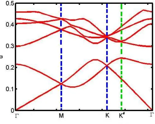
To calculate the bandstructure for such a waveguide, we use a supercell consisting of many periods of the unit cell, and then delete a hole to form the defect. However, because we wish free propagation in the ΓK direction, the supercell must be only one period wide in this vector. As a result, we must have a rectangular supercell, containing several holes, and hence we now calculate a projected bandstructure. In figure 2.2, we calculate the bandstructure for identical parameters to the above, but now using a rectangular basis. The first figure is much simpler, but the second can be understood in terms of zone folding from the first. The point indicated as K′ is the high symmetry K point for the supercell in the triangular basis, and for our defect waveguides, it is at this point that folding effects occur. For the mathematics, see [14], or for a geometric approach [15]. Finally, in figure 2.3, we show a typical bandstucture for a W1 waveguide, with the various regions of interest indicated. The bandstructure is restricted to ΓK, because we are solely interested in propagation in this direction, hence the presence of an omnidirectional bandgap is not important.
In the figure, the air and silica lightlines are shown - the lines ω =ck and ω =ck/nSiO2 for suitably normalised ω and k. These are used to express the
Figure 2.2: Bandstructure for a triangular lattice of holes, using rectangular basis
vectors as opposed to the natural unit vectors in the previous figure. The
supercell now contains two holes, so some otherwise degenerate bands are
duplicated at other points in the dispersion diagram. Appropriate folding of
the Brillouin zones returns this figure to the simple form above. The point
marked K′ is important, as this is the projected point equivalent to the K point
for a unit cell containing a single hole.
closely follows the fundamental mode on its first pass between Γ andK, before it folds back. As a result the folded-back PhC mode in the band-gap is not TIR guided at all, but instead radiates for all frequencies.
Figure 2.3: Bandstructure for a W1 waveguide in a triangular lattice of holes, using
rectangular basis vectors. We now only consider the Brillouin zone between Γ
and K. The fundamental mode is magenta for normal propagation and blue
in the slow light regime; the fundamental mode below the bandgap is green (see
chapter 4), and the lattice regions are outlined in black. The two heavy black
lines are the air and silica lightlines.
the fast or index-guided mode, whereas the blue slow-light mode is gap-guided. The transition between these two regimes is smooth, and the reasons for them are explained in detail in [16].
2.2
Maxwell’s equations
After the conceptual introduction above, we now return to mathematical analysis, starting with Maxwell’s equations. These are given here for reference, particularly for the descriptions of bandstructure calculations using planewave and finite-difference-time-domain (FDTD) methods which will be discussed in subsequent sections.
div(B) = 0 (2.1)
div(D) =ρ (2.2)
curl(H) =∂tD+J (2.3)
curl(E) =−∂tB (2.4)
Using the standard symbols - E is the electric field, Hthe magnetic field,
Dthe electric flux density, andB the magnetic induction. For linear materials
B =µH for magnetic permeability µ, and D=ǫE with ǫ=ǫ0ǫr representing
electric permittivity. ǫ0 is the free space term; commonly I will work with
the refractive index n = ǫ0.5
r for pure dielectric materials. ρ and J represent
free charge and current densities respectively. For the systems studied in this thesis, we assume that there are no free charges, hence:
that the magnetic permeability µr= 1, and that the dielectrics are purely
real, therefore:
div(H) = 0 (2.6)
ǫ div(E) = 0 (2.7)
curl(H) =ǫ ∂tE (2.8)
curl(E) =−∂tH (2.9)
2.3
Practical numerical modelling of photonic
crystal slabs
In the introduction to PhCs above, I have stated that there are periodic solutions to Maxwell’s equations. As with normal waveguide modes, these periodic solutions are transcendental, and so must be found using numerical methods. There are a variety of techniques for doing this, which have different strengths and weaknesses in terms of application for designing PhC based devices. It is this application which I will discuss here, rather than either the details of these techniques, or even the theoretical considerations leading to these solutions. For the latter, refer to [4].
these methods to determine useful structures. Further, one can be confident in one’s results only when they can be obtained using a variety of methods.
In this section, I will consider first frequency and then time domain methods, and for each of these discuss how bandstructure and transmission spectra can be determined using a variety of commercial and freely available packages. This only covers techniques I have used significantly, as an overview of other alternatives is provided in a subsequent section. For each of the techniques here, the aim is to explain the criticalities in its use, and the relative merits of the method.
2.3.1
Frequency Domain Techniques
We begin by considering frequency domain methods - in general, to use these, it is necessary to understand the problem and the expected result, to try and calculate an intelligent and (semi-)analytic solution. The benefit of this prior effort is that the result is relatively easy to interpret, as it will be in terms of modal eigenvalues and eigenvectors, and further using some analytic results can both improve accuracy and reduce simulation times. The disadvantages are that the method used must be targeted to the system of interest; there are no completely general frequency domain techniques. Also, results may often be for single frequencies or k-vectors and only give steady state responses, making it difficult to see how a system performs over time[17]. It is often claimed that frequency domain methods are faster, but this is only true for specific systems, and frequently not the case for PhC device modelling.
2.3.1.1 Bandstructure Calculations
basis vectors that describe the dielectric structure and the fields. However, there is a strong preference for the planewave technique, as the dependent variable is the k-vector, whereas in eigenmode the dependent variable is the frequency - and therefore it is a resonance-finding method, which we prefer to implement in FDTD (see next subsection). For a complete discussion of the eigenmode method, see reference [18].
For the planewave method, there are two options readily available at St Andrews, namely the MIT photonic bands package (known as mpb) [19, 20], or Photon Design’s bandsolver package [21]. Although the detail of the code is of course different, the underlying algorithm is the same, and so the packages are often used interchangeably. To confirm this, figure 2.4 compares the (2D) bandstructures calculated for a typical W1 waveguide2
in each package. mpb uses a completely periodic supercell technique, although the dielectric function is discretised in real rather than Fourier space. Photon Design, on the other hand, allows the use of an absorbing boundary condition, but only in the out-of-plane direction for the 3D bandstructures of PhC slabs. It is commonly thought otherwise! As a result, the supercell size used for 2D calculations is significant. In mpb we typically use a supercell with 18 periods of PhC transverse to the propagation direction3
, but the graphical nature of Photon Design encourages smaller supercells. In the figure, I have used the different typical parameter values for resolution and supercell size, and as a result the calculations are more different than would be expected based on Photon Design’s validation documents4
.
2
The parameters are the same as in chapter 4
3
Determined by S. Boscolo of the University of Udine to have no significant coupling
between parallel waveguides in the real space representation for this resolution.
4
Figure 2.4: Comparison of 2D bandstructures calculated with the mpb and Photon
Design bandsolver packages, for a W1 waveguide. The calculation is performed
with a grid resolution of 20 in mpb, which is optimal, and 36 in Photon
Design as only powers of 2 are permitted. The nature of the packages
encourages different supercell sizes, so for accurate results care must be taken
with convergence. The different band positions apparent in this figure are
mainly related to the different supercell sizes.
Planewave algorithm For a detailed mathematical treatment of the algorithm, the reader is referred to [19], and the relevant manuals. Here, I will try to provide a sketch of the process, mostly derived from the manual for mpb.
In a planewave model, the bands of a PhC are computed as eigenmodes of the dielectric system, using Helmholtz’s equations:
curl(1
ǫ curlH)−( ω
c)
2
= 0 (2.10)
E=−(ic
ωǫ)curlH (2.11)
as:
H=Hk(x)eik.x (2.12)
Where Hk is a periodic function. This is equivalent to saying that the calculation has periodic boundary conditions. To solve 2.11 numerically, we then expand Hk in a Fourier basis, as a sum of planewaves. To multiply by the inverse dielectric function Hk is Fourier transformed into real space, and the desired PhC discretised accordingly. We then return to the frequency domain to solve the eigenvalue equation, using iterative methods as we only desire a small number of the eigenvalues of the matrix. The key to a good planewave algorithm is in the discretisation of the dielectric function, because this impacts strongly on the time to convergence in the iteration. In both mpb and Photon Design, it is difficult to know exactly which dielectric function has been used, because the discretisation is optimised in many ways. The number of planewaves required to achieve convergence is strongly dependent on the disctetisation of the dielectric function, but we do not explore htis further here, as we only wish to use the available tools effectively. Because we calculate eigenstates, the overhead to calculate field profiles and group velocities is minimal. Hence, we can have all of this information from one calculation, which is not possible using time domain techniques.
3D Bandstructures We can also extend this to 3D, but for PhC slabs, there is a problem. As discussed, mpb simulations necessarily give solutions which are periodic in all directions, and so we must also consider an out of plane periodicity which is very unphysical5
. To do this, we can define our slab
5
I have been unable to test 3D bandstructure calculations in Photon Design due to
structure in a large supercell, with a large volume of air above and below. In principle, for a low out of plane contrast system, we could instead fill space with a high index material. For the high contrast case (e.g. SOI), we can then easily compute the true modes, those that are fully guided by the slab (i.e. below the light-line). The leaky radiation modes can also be calculated, but this is more complex. Consider: the mode tail for the radiation mode extends out of the slab, and only becomes negligible at a certain distance. If there is any significant field, it may couple into the slab mode in the next repeat of the device, or it may reflect from the interface and come back. Either way, the result is non-physical. To reduce this problem we need to use very large supercells, and the computational burden becomes beyond our capabilities. Instead, it is possible to perform the calculation with relatively low air volumes. In this case, we have to consider modes guided in the substrate, modes guided in the air, and glancing angle modes, all of which are purely a result of the boundary conditions. This can be done, by outputting the mode profile in some way (e.g. the flux density in the guiding layer) and filtering the bandstructure data accordingly, but this has not been attempted. It was found easier to use an FDTD method with absorbing boundary conditions (see later). An alternative approach is to insert an absorbing medium into the out-of-plane dielectric profile, as has been done in Photon Design’s Crystalwave, however I have not evaluated this.
2.3.1.2 Transmission and Phase
Design’s FimmProp and Omnisim frequency domain engine [21]. Of these, only FimmProp is a fully 3D solver, and it has only been used incidentally in this project.
The CAMFR and FimmProp codes are based on the principles of Eigen-mode expansion, detailed in [18]. The structure is discretised into transverse slices, which are then stacked together in the propagation direction to form a device. The solver calculates the modes for each slice, propagates the mode (actually simply rotates the phase) for the desired length, and then performs the overlap integral between each adjacent slice. This is implemented in a scattering matrix algorithm, to take account of forwards and backwards propagating modes in a numerically stable fashion (compare transfer matrix). For simple waveguide devices and grating couplers, this is a very useful approach, because it scales with the number of different slices, rather than the area covered by the device.
field is forced to zero. Both of these methods are simple to implement, and both can be easily used to divide a simulation in two along the propagation direction, forcing propagation in odd or even modes respectively. However, at the edges of the simulation, these methods can cause reflections back into the simulation space, that in real life would decay away.
PML To solve this problem, we have the perfectly matched layer[23]. Essentially this is an absorbing layer placed between the edges of the device and the wall. This is more difficult to implement in practice, but is a necessary technique. However, the mathematics of absorption cause the problems associated with PML. If we consider a real evanescent mode of the formE0eωt,
and multiply by an absorbtion e−αL, then the amplitude will reduce; and we
can set α and L such that there is no significant field at the boundary. But, for example, assume that we have a propagating photonic crystal mode with a significant intensity in the lattice and hence close to the boundary. We now have a field of the form E0eiωt, which will decay more slowly, and then
reflect from the wall and re-enter the simulation. Depending on the method in which the PML is defined, it can even experience gain in some circumstances. Essentially, then, we need to first of all run a simulation for a single transverse slice of the structure, and vary the PML position, width and strength until the result is stable. A photonic crystal already has a high transverse width, and so the already large simulation must become even greater for reliable simulations in this scheme. Ideally, one must have a good idea about the modes and their properties before starting such a simulation.
profile is instantly available, as is the amplitude and phase at any point in the simulation. This data is, of course, also obtainable in the time domain, but suffers more strongly from numerical noise, and must be extracted via arduous post-processing.
Photon Design’s Frequency Domain Engine In addition to these, we have Photon Design’s 2D frequency domain engine. This is a proprietary finite element technique with an adaptive grid, rather than a mode solver. However, it provides results similar to CAMFR: the mode at a given frequency of the entire system (not slices), and the relative amplitude and phase between any two points. This program is very simple to use, unlike CAMFR where discretisation must be taken care of by the user, and often solves systems very quickly. In particular, this program has been used extensively in my work on tapers (chapter 4). Unfortunately no information is available on the algorithm it uses, so I cannot describe it. However, results for simple systems compare well with those calculated using FDTD in the same package.
It was also hoped to use this package to complement the PhC coupling results in chapter 5, particularly to prove the effectiveness of the tapered crystals discussed there as a solution to the slow-light coupling problem; however, the predicted memory requirements for the necessary simulations approach 10GB RAM, hence it was not possible to complete this work.
2.3.2
Time Domain Methods
it is relatively easy to understand what your simulation is doing. Calculations can be set up quickly, and changing systems is easy. However, only the amplitude of a field is readily calculated, saying little about mode properties. To compensate for this, for PhC devices it is important to start and end time domain calculations in a simple ridge waveguide, so that at least you can calculate an overlap integral with the waveguide mode. Many groups consider FDTD results as a numerical experiment.
2.3.2.1 Bandstructure Calculations
For the time domain methods, it is more usual to start by discussing transmission techniques, as these are the usual application of this method. However, for the sake of consistency I will start with bandstructures.
Firstly, though, we must understand how the FDTD algorithm works. We have previously shown Helmholtz’s equations 2.11, which is derived from Maxwell’s equations by assuming solutions which are sinusoidal in time, and said that it can be solved numerically. In FDTD, this is done in the following way [24]:
1. discretise the dielectric profile onto a regular grid
2. implement the Yee cell6
3. impinge a magnetic (electric) field
4. calculate the electric (magnetic) field via the curl equations
5. increment the time step
6. calculate the magnetic (electric) field via the curl equations
7. repeat from 4
To illuminate this, refer to Hagness [24] or Min Qiu [25], from either of whom FDTD codes and algorithms are available7
. I have worked almost exclusively with commercial codes, and so will offer only the limited perspective needed as a user, rather than developer, of FDTD methods.
Beginning with 1, we have to consider our device not as a slab with some holes etched into it, but rather as a fine mesh, in which different cells have a different dielectric constant. In our device, we have ǫdielectric and ǫbackground,
but in a 2D calculation we use the effective index of the slab ǫslab, and ǫ0 for
an air background. Each cell in the mesh overlaid on the device will contain either air, or slab, or a proportion of both, and we model the “both” with
6
explained subsequently
7
an intermediate dielectric constant. The size of the mesh must be adjusted to give a sufficiently good representation of the structure, via convergence testing, howeverperiod/20 is a good rule of thumb for photonic crystal devices. Commercial codes also implement sub-gridding to increase the resolution of small features.
Figure 2.5: One period of a 2D Yee cell. The electric and magnetic fields are
calculated on separate interspersed grids.
response and so must be run for a long time to a steady state.
The remaining steps (4 onwards) calculate the evolution of the field as it propagates away from the launch. This is numerically simple in principle, especially on the Yee cell. The curl is the circulation of the field, so recalling:
curl(E) =∇×(E) =
ˆi ˆj ˆk
∂x ∂y ∂z
Ex Ey Ez (2.13)
which expands as:
curl(E)) =ˆi(∂yEz−∂zEy)−ˆj(∂xEz−∂zEx) + ˆk(∂xEy −∂yEx) (2.14)
If we consider a one dimensional system for the sake of simplicity, then ∂x
and ∂y are zero, and we obtain:
curl(E)) =−ˆi∂zEy+ ˆj∂zEx (2.15)
assuming propagation in z.
Now, recalling Maxwell’s curl equations:
curl(E) =−1
c ∂t(H) (2.16)
curl(H) = ǫ
c ∂t(D) (2.17)
The magnetic field at t+ ∆t can be written as:
H=c(ˆi∂zEy−ˆj∂zEx) ∆t (2.18)
hence:
Hx =
Eyz+∆z/2−Eyz−∆z/2
Hy =−
Exz+∆z/2−Ez−
∆z/2
x
∆z ×c∆t (2.20)
where ∆z is the spatial step, or grid size. The ±∆z/2 refers to the interleaved grid of the Yee cell. Given H, we can write a similar equation for E. These can be extended to a full three dimensional form on the same principles. We can then continue to computeE and Halternately for as long as is desired.
In this equation, ∆t and ∆z cannot be arbitrary - instead, they are linked by the Courant stability condition. Essentially ∆z cannot be greater than the distance that light can propagate in a time ∆t, in the appropriate medium.
So, the result of the FDTD algorithm is to reduce the process of solving Maxwell’s equations to simple arithmetic. Of course interesting effects arise, making FDTD an active area of research - seewww.fdtd.com to see the current scope of this! There are several sources of complexity, including boundary conditions, efficient computations, and reducing the sheer volume of computer memory required to perform these calculations over a significant device area, amongst others.
FDTD Bandstructures After this whirlwind tour of the principles of FDTD, we return to the question of bandstructures and periodic boundary conditions. As we clearly introduce a frequency into the system with the incident field, the boundary must allow a method to find the k-vectors for any particular frequency. In chapter 4, we will consider a k-vector as an angle, and it can also be considered as a phasor. Dealing with the simple case of propagation along a waveguide, we know that k=p
k2
x+k2y+kz2 is a
particular angle, and that kz is the component of that angle in the direction
field at the leading edge of the supercell to the field at the trailing edge, plus a phase rotation according to the desired k-vector. The simplest case is at the Γ point, where the rotation is zero.
Previously, we have said that a field must be introduced slowly, but at a boundary we introduce on the left hand edge exactly the field calculated on the right hand edge at the previous time step. We do this by adding this set of values to the existing set before calculating the next evolution of the field. We keep doing this, and advance the time step until we reach a steady state condition. For frequencies where the both edges of the simulation are in phase, the system resonates, but all others will die away rapidly. We can determine these frequencies by using an input field with a broad spectral range, and monitoring the variation of the field with time. The Fourier transform, or better yet harmonic inversion [20] as the signal is decaying, yields the frequencies. This is then repeated for other k-vectors.
There are several advantages and disadvantages to this method. At first sight, the disadvantages seem overwhelming. Firstly, it lacks the mathematical elegance of the planewave method as described in the previous section. To find the field profile the simulation has to be repeated at the appropriate frequency. The results are noisy, even using harmonic inversion, so repeated simulations with narrower launch bandwidths have to be used to home in on precise values. The group velocity isn’t intrinsically calculated. FDTD is a brute force method, and hence strictly limited by the RAM available, and the post-processing required to extract the frequencies is similarly computationally expensive. Finally, we have to work in real space with real frequencies.
of the bandstructure we’re interested in. More important, though, are the possible boundary conditions for bandstructure calculations. By using a PML in the transverse direction, we can have a supercell significantly smaller than those required for the plane wave method. Further, we can extend to 3D trivially (excepting memory requirements). By also using PML in the out of plane direction, we do not have the box mode problems that exist with plane wave, so we can solve for guided resonances above the lightline as easily as guided modes below.
2.3.2.2 Transmission and Phase
As with the bandstructure discussed above, in the time domain we typically calculate transmission using the FDTD approach. We do this simply, using the same algorithm as above, but instead of a supercell and periodic boundary conditions we lay out the dielectric profile of the entire device.
The two commercial codes we typically use, Photon Design’s Omnisim [21] and RSoft’s FullWAVE [26] 8, have slightly different implementations of the
basic FDTD algorithm. With Fullwave, we can only determine the net field at any given point, whereas Omnisim gives access to the forwards and backwards going flux as well. However, with either approach, it is challenging to obtain accurate phase information, yet this is necessary to study the effects of the interfaces of our devices. This is discussed more fully in chapter 5. To obtain this information, in principle one could simply look at the phase from the Fourier transform of a pulsed simulation. Unfortunately, this phase is not well defined, because only the pulse centre-frequency is correctly launched in the appropriate well-defined waveguide mode, and we need a very high degree of accuracy in the phase, because the group velocity effects we are interested in
8
are calculated using the second derivative of this phase [15]. The only method which has been found to be acceptable is to run cw calculations to a steady state, and then fit a sine wave to the last few hundred periods of the response. Then we must scan the required spectral range in sub-nanometer steps. This is hugely time-consuming, and has been a major limitation on the theoretical work in chapter 5.
2.4
Conclusion
In this chapter, I have explained the terms used to describe the PhC design work later in this thesis, such as lattice regions and slow light, and showed the origin of these effects. Thereafter, I have discussed in detail the calculation methods that will be used throughout the rest of this thesis to design devices and study their behaviour. These methods are derived very briefly; with emphasis on the practical application of the methods used, their individual strengths and limitations. I stress again, no single method is completely to be trusted, instead one seeks agreement from a variety of calculations.
Chapter 3
PhC fabrication techniques
3.1
Introduction
3.2
Substrate choice
As there is no wafer growth at St Andrews, this section is included merely for completeness. For the devices detailed in other chapters, I have used three particular wafers - SOI with 220nm silicon over 1000nm (or more) silicon oxide on a silicon substrate; 200nm Q1.22 InP on an InP heterostructure designed to be removable after wafer bonding; and a complex AlGaAs heterostructure. These have been sourced from various suppliers, and the wafer designs form part of other projects. Clearly, the choice of wafer is dictated by the application, and governs the fabrication processes.
In each of these, the critical part is that the guiding layer (top for InP and SOI, buried for AlGaAs) is single moded at telecoms wavelengths, which has been verified in each case by the wafer designers, F. van Laere at Universiteit Gent, T.J. Karle and T.F. Krauss at St Andrews. The layer structures are shown for SOI and AlGaAs in figure 3.1; for InP refer to chapter 4.
Figure 3.1: Layer structures for the SOI (left) and AlGaAs (right) used for the
devices in later chapters (not to scale). The layer compositions are indicated
as well as typical etch depths.
either system, albeit by different methods.
3.3
Masks
A mask is an intermediate step between the device you design and the device made. For Si processes we typically use the lithographic resist layer as the etch mask. I have tried using an oxide based hard mask as part of the process development. However, in our RIE the mask etches away faster than the silicon for PhC features of 100s of nm size, and as such is useless.
For non-Silicon (heterostructured AlGaAs and InP) fabrication, etching the pattern requires a hard mask to be deposited on the substrate. This is because the ion-beam etching is very selective to dielectric masks and the etch depth required may be great (>2µm), and perhaps most importantly, the etch chemistry necessitates a high temperature process. In the case of shallow InP etching, I did attempt to use only a soft mask. Although it actually survived the very short etch time, it seems to have softened such that it flowed back together, deleting the pattern!
3.3.1
Hard masks
resistant, but the thinner mask does not. However, this is conjecture.
The sol-gel process has been developed for use in house, and involves a spin-coating technique to deposit the film. The chemistry of the sol-gel is not relevant here, as we use a commercial product FOX-14. When suitably spun and baked (at very high temperatures, up to 500oC), it provides a silica-like
hard mask. Each layer is typically 140nm thick, and in principle multiple layers can be deposited, to give the required mask thickness. However, I have not found this material to show the non-linear selectivity of the PECVD material, so a thicker mask is required. The HSQ is preferable in cases where electrical contacts are required at a later stage in the processing [27].
3.3.2
Lithographic resists
A resist is (typically) a polymer film deposited via spin-coating and baking at low temperatures, typically 100 to 200oC. The film is altered in some
way by the interaction with photons and/or electrons, by becoming either more (positive) or less (negative) soluble in its developer solution. As such, resists are used for pattern definition, and as etch masks for some processes. As with hard masks, the critical parameter is thickness, although in this case I found that multiple layers cannot always be used to increase the film thickness. Instead, solute concentration or spin speed must be altered appropriately. This would seem to be solvent-related. Specifically for the ebeam1 resist polymethylmethacrylate(PMMA), our standard solution is a
mixture of commercial PMMA and a thinner. With hindsight, it seems clear that the PMMA will readily re-dissolve in the thinner!
The typical soft masks are this PMMA and the proprietary ZEP-520A (commonly, ZEP) which are ebeam resists. No significant optical lithography
1
has been used here, so optical masks will be neglected. With both of these resists, it is necessary to consider the required sensitivity to the ebeam exposure. Although this decreases only slightly with mask thickness, it is easier to accurately define a PhC with a thinner mask. Of course, possible etch depths increase with thickness. For the narrow lines and large holes needed for my InP work, it is necessary to have a very thin mask, to achieve sufficient control of feature size. On the other hand, for my SOI etching, it never became possible to make a thick enough film of PMMA to reliably etch the silicon layer well, and as a result it was necessary to switch to ZEP. This will be discussed further in the etching section.
3.4
Lithography
The desired pattern is defined in the chosen resist in the lithography step. As I typically need sub-100nm resolution, I use ebeam. The major pattern definition tool used in this project is a Raith Gemini electron beam system. Although installed at St Andrews several years prior to the beginning of this project, a huge amount of detailed knowledge and experience was required to make the devices for this project, and has been developed over the course of (although not as part of) this project. Almost all of the credit goes to D.H Brown and L. O’Faolain; but again I will emphasise my contributions.
Some additional electron beam lithography was also performed at Glasgow University on their Leica EBPG-5 semi-commercial tool.
resulted, so I will not discuss this further here. For details of this process, see [28].
3.4.1
Electron beam lithography
Ebeam, more formally known as electron beam lithography, is perhaps the most important technology for PhC fabrication. By using high energy electrons rather than low energy photons to expose the resist, the degree of control over pattern definition considerably improves, and as a result the minimum attainable feature size decreases.
Although a detailed review of the theory of ebeam lithography is beyond the scope of this thesis, a discussion of the process from a user’s perspective is illuminating - since this is the level at which we have mastered our system. For details of the theory, see [29], and the system manuals. Also worth a read is the user manual which has been developed in house. I then present a discussion of the techniques that I have helped to develop, which have been critical to fabrication success in this project.
3.4.1.1 Process flow
This is provided for reference purposes, as it is very specific to our current system. However, it is useful to provide context for terms which will be used later.
1. Load sample
2. Wait at least one hour, to allow stage drift to stabilise
3. Measure beam current
5. Correct focusing, stigmation and aperture alignment at very high magnification (greater than 100,000 times)
6. Burn contamination spot 2
7. Align writefields, ideally using a contamination spot
8. Expose pattern
Doing all of this correctly can take quite some time! When writing small numbers of large features, this process can be very simple. But to successfully write a set of photonic crystal devices, the process breaks down into a large number of smaller steps, each with their own complications. Subsequently, I will discuss the interesting ones.
3.4.1.2 Beam currents, beam speeds, and step sizes
In the process flow step 3, “measure beam current” sounds very simple. In fact, as a process, it is! However, the next part, setting step sizes and dwell time is rather less so, and depends strongly on the measured current. These values affect both resolution and stitching issues. The former is important for my work on elliptical holes, the latter for making access waveguides to bring the PhC-matched waveguide mode up to an easily measurable scale.
Consider firstly resolution: we operate with a fixed beam current, and write on a resist with a fixed clearing dose, where dose is equal to current × time /area, typically in µAs/cm2
. Clearly, there is a physical limit to
2
This is very specific to Raith systems - it translates to exposing a single point and
watching the behaviour of the beam current on a picoammeter. As the point is exposed
-burnt - its conductivity changes and the current falls. The rate of current decrease and the
size of the resulting contamination spot show how well the focussing etc. have been done,
how quickly the beam can move, or be switched off. As a result, there is a minimum area that can be exposed - this is known as the step size for the raster scan. Initially, our ebeam lithography was done with the beam area and hence current constricted by a thirty micron aperture. In figure 3.2, the pattern was defined using the minimum step size possible with this aperture. The pattern is an elliptical hole with a constant air filling factor, replicated over a square lattice. The bottom left ellipse is at a 45 degree angle to the lattice vectors, and is rotated across the lattice such that the ellipse is vertical at the top left and bottom right. The important point is this: in the SEM image, the air filling factor is not constant. The reason for this is the discretisation involved with the raster scan at the minimum step size; which is sufficient to vastly distort the filling factor.
To solve this problem, we clearly must further reduce the step size. To do this, the only choice is to reduce the current. We do this by reducing the aperture, and hence the beam diameter. Figure 3.3 shows a pattern for a real device, written with 30µm, 20µm, and 10µm micron apertures. The 10µm pattern has the highest definition, but takes longest to write.
Figure 3.2: SEM image showing the effect of discretisation. The dose is increased
from left to right. In each block, we have a lattice of identical elliptical holes,
which are increasingly rotated in each row and column of the block. In each of
the four rows in the image, the rotation angle of the first hole in the block is
increased. As a result, the over-exposed area moves for each row. This image
conclusively demonstrated that the minimum step size achievable with a large
aperture cannot be used to write holes with a controllable shape.
Figure 3.3: A real device, which needs definition of hole shapes and hence very
accurate lithography. The top and bottom halves contain PhCs with elliptical
holes, with eccentricity 1.5 and rotation of 10o and 50o respectively. The
ebeam aperture is increased from left to right. The definition of the hole shapes
a disadvantage; firstly that the system needs to be focused individually for the two apertures, and secondly that they need to be brought into alignment with each other. The former effectively doubles the set up time, and the latter can introduce errors as perfect alignment is not trivial. However, these are much less troublesome than the step size and writing time problems, so changing apertures is now commonly accepted as a viable compromise.
Stitching Moving on to the issue of stitching, which is part of the “complexity” mentioned above. Briefly, to write a pattern, you can define a small area called a writefield, which can be exposed by raster-scanning the beam. The area over which the beam can be rastered is mechanically limited, and also computationally limited. The computational part is trivial -a digit-al to -an-alogue converter is used to convert between the digit-al file -and the analogue motion of the beam, and the DAC only has a certain number of bits and hence quantisation levels. Hence, regardless of the current/ aperture issues, the minimum step size is related to the size of the writefield. The optimum for our system, considering many other variables, is 100µm - to write larger patterns, the stage must be moved. The stage position and motion are controlled via feedback from laser interferometers, with a mean theoretical error of 40nm. To achieve this, there are alignment routines that must be followed. However, this 40nm error is not typically seen in ridge waveguides that are written, because there are other effects that dominate.
is taken to keep the beam speed below 5mm/s, the lower the better. For a small aperture, doing this requires increasing the step size above the minimum possible - so again, we use an aperture changing technique, using a moderate aperture and large step size (hence low beam speed) to write long waveguides, and a small aperture and small stepsize to write fine details. Long photonic wires, which need both fine control and good stitching are best avoided, unless an additional technique I have discovered is used: break all large areas up into many contiguous small areas! The software then adds a beam settling time to the exposure for each polygon, reducing the effective beam speed over the waveguide, and hence improved stitching, regardless of step size.
There is an additional problem that has been found, that for many years was thought to be a stitching error. Again, this is a software limitation. In my process flow above, one step is “leave for one hour, to allow thermal drift to stabilise”. But, in practice there are two effects, the drift of the stage as it settles to the mean temperature of the system, which affects focussing and stigmation, and also the beam drift, which is continuous and periodic, with a period of several minutes. An example of the error is found in figure 3.4.
Figure 3.4: Pseudo-stitching errors caused by out of order writing. The left hand
image is a cutaway from the right, taken at the same scale but reproduced here
at a higher magnification, to make the defect more obvious.
The device pictured is a PhC with increasing crystal period at each end of a
This occurs when the PhC pattern is not written in a canonical order - so two adjacent rows of holes are written at different points on the bean drift cycle instead of continuously. This is a significant error, on the order of 200nm in the worst case - because a 5nm change in the position of a row of PhCs is used to create a so-called heterostructure cavity [30]. The error is actually caused by the memory limitations on the proximity correction process - as the whole pattern cannot be held in memory at once, the pattern order gets jumbled! Figure 3.5 shows the same device written correctly. Proximity correction is discussed in the next section.
Figure 3.5: The same device, with the holes written in canonical order. The beam
drift no longer induces stitching errors. I designed these devices, but thanks
to G. Pagnotta for writing the code which fixes the problem.
An alternate method to remove all stitching errors is a technique known as shot-shifting which is also used to remove statistical disorder in the PhC lattice, but has not been not used here [31, 32].
3.4.1.3 Spots
the smallest useful feature for write-field alignment, and as such the greatest accuracy in alignment is gained when using this spot. To use aperture changing techniques, this accuracy is necessary.
In figure 3.6, there are two images of these spots, one on SOI and one on InP. The much greater visibility of the SOI spot lends itself to complex writing techniques, but with the poor visibility InP spot, we are restricted to 20µm or greater apertures, and so cannot use aperture changing techniques. This is significant for the work in chapter 4.
Figure 3.6: Spots - on InP on the left, and on SOI on the right. The much greater
visibility of the SOI spot makes writing on SOI easier, and also allows the use
of multiple-aperture techniques. For the InP, we are restricted to apertures
greater than 20µm, because with smaller apertures contamination spots are
not visible.
3.4.1.4 Dose to target
It all comes down to stray electrons. With a PhC lattice, backscattered electrons and other secondary exposure mechanisms give rise to a low level exposure away from the feature currently being written, no matter how carefully the dose is selected. This low level exposure is also developed, so a feature is always larger on a sample than on the mask. How much larger is related to the developing process, but as examining the results here is challenging, it is simpler to have a consistent developing process and control the hole size lithographically. To manage the backscattering effect, it is quantified as a background level for the nearest neighbour holes. In a triangular lattice, a central hole receives a background dose contribution from each of its six nearest neighbours, whereas one on the edge of a pattern may only have two contributions, and an isolated hole none. As a result, a proximity correction algorithm assigns a low dose to the central hole, a larger one to the edge hole, and larger yet to the isolated case. This is easy to understand, but to calculate the effects requires a very computationally intensive algorithm [33].
the desired pattern.
[image:57.595.249.365.325.448.2]This dose to target effect is also useful for isolated lines and one dimensional gratings, simply as over-exposure tends to give the smoothest possible lines. Photonic wire bends are similar. The effect of raster scanning on a bend is to make it rather uneven because of the square grid at the step size; so the width varies around the bend. To make a smooth bend, so the width varies around the bend. To make a smooth bend, over-exposure is necessary, and to make a smooth bend of the desired width, dose to target techniques must be used. Some examples of photonic wire bends are shown in figure 3.7.
Figure 3.7: A variety of bends. The first is written using a large step size, and
critically exposed. In some areas, the bend closes up completely. The zoomed
image shows the roughness of the bend. The second bend is written using an
overexposure technique, and is both continuous and smooth.
3.5
Pattern transfer and etching
to explain the parts where significant development work has been done, and where my processes provide substantial benefits.
3.5.1
Heterostructure devices
For this project, two significant heterostructure devices are involved, namely a PhC y-splitter et al. (chapter 6) on AlGaAs, and a surface grating coupler on InP (chapter 4). The techniques used in etching these two devices are fairly similar. In both cases, we use PMMA as the resist, and transfer into a hard mask using RIE (Reactive Ion Etching) in a fluorine chemistry, and then etch the pattern into the heterostructure using CAIBE (Chemically assisted ion beam etching) in chlorine chemistry. For the AlGaAs patterns our concern is to maximise the etch depth, whereas achieving exactly the target etch depth is important in the InP case.
The pattern transfer step is the most standardised of all the fabrication processes used here; and poor results are usually due to external effects. There are two limits to this, firstly that the RIE machine is used with other etch gases which can cause contamination that affects the etch recipes, and secondly mask thickness. Although the standard recipe is consistent, the selectivity is 1:1 at best. Using a thicker hard mask to get a greater CAIBE etch depth requires a thicker resist, and this lowers resolution in the pattern. The etching is done in CHF3 gas, taking about 15 minutes for 300nm of silica hard mask.
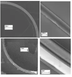
sample temperature, the velocity and number of argon ions for the mechanical etching component (via beam voltage and current)and the relative number of argon and chlorine ions available for etching. There are several regimes that can be optimised to give good results, some examples of which are shown in figures 3.8 and 3.9. For a detailed discussion of this, refer to M.V. Kotlyar’s thesis [37], and L. O’Faolain’s thesis [38].
Figure 3.8: Good quality AlGaAs etching in CAIBE for the Y-splitter devices in
chapter 6. The etch depth and sidewall verticality are the critical parameters
to optimise.
3.5.2
Silicon etching
The silicon etching here is primarily SOI rather than silicon wafers, and the typical SOI is a 220nm Si guiding layer on 1µm buried oxide (BOX), over a silicon substrate. For PhC devices, Bogaerts et al. [28] have shown that simply etching holes into the top silicon layer, and neglecting the BOX, gives the best results consistent with the additional difficulty in transferring the pattern into the oxide. One can also make a silicon membrane, by using a wet HF process to undercut the PhC device. Although there are arguments for and against this, it has not been done in this project.
Figure 3.9: Shallow InP etching in CAIBE, for an attempt to realise the 1D
gratings in chapter 4. The etch depth in the figure is close to 95nm. In
this case, we have to accurately hit a target etch depth while maintaining good
etch-floor roughness and sidewall verticality. This is the best result I could
achieve, which manages two of the three requirements. However, CAIBE is
not well suited to shallow etching, and so we have changed to an ICP system
for these devices. This is discussed further in chapter 4.
and SF6 gases. The SF6 gas etches the silicon, but it does so in an isotropic
fashion which is not very conducive to PhC holes with vertical sidewalls. CHF3
is added to provide directionality; it reacts with the product gases to form a polymerisation layer, and so prevents etching outwards.
The challenge with silicon etching in this kind of process is in the masking. In the pattern transfer process, we can use 200nm of PMMA and etch for 15 minutes, which indicates that PMMA resists CHF3 gas well [39]. Using a
similar etch pressure but replacing half of the CHF3 flow with SF6, we find
that the 200nm mask lasts less than a minute, and the silicon is only etched to around 100nm. All values given here are very approximate, as it depends strongly on hole size, and the accuracy of depth measurement is limited - the SiO2BOX layer is an insulator, so charging effects in the SEM reduce precision.
make small holes, and difficult to accurately control hole size. Clearly, an alternative solution is desired.
[image:61.595.250.362.389.506.2]Although several attempts were made to alter the etch chemistry, none were successful. Instead, the resist type was changed, from PMMA to ZEP, following the practice of several other groups fabricating PhCs in Si. This improves the situation somewhat, although the result still is not perfect. We can reliably etch holes of diameter greater than 200nm all the way through the top Si layer. For a typical target r/a of 0.27, this gives a minimum period of 370nm, which is acceptable for devices designed to operate at 1550nm, but only just. Further increases in resist thickness are not desirable, so work is in progress on further improving the process. An example of etching is shown in figure 3.10.
Figure 3.10: RIE etching of PhCs in SOI, using a mixture of SF6 and CHF3
gasses. The aim is to etch through the 220nm top Si layer only, while
maintaining sidewall verticality.
has improved with the experience of the group, by learning which details must be taken care of3
, and now only a few samples are lost.
3.6
Additional processes
As well as the processes described here, there are many others that are routinely undertaken, and that I have helped to develop, such as those for sample cleaning. These fall under the heading of tedious in the introduction to this chapter. However, there are additional interesting processes, particularly the wafer bonding used in making the InP grating couplers, which are very specific to particular devices, and as such are discussed in the relevant chapters.
3.7
Conclusion
In this chapter, I have discussed fabrication techniques used in making the devices in the other chapters, specifically showing the problems I have encountered, and solutions discovered by myself and colleagues. The most significant technologies, or at least those that I could most influence, are the ebeam lithography used to define the device patterns, and the dry etching used to transfer these patterns into the various material systems used. I have done lithography and etching on InP, GaAs, and SOI platforms, each of which presents their own different challenges. Both my own work and that of my colleagues towards overcoming these has been presented. With due care and attention, we have the tools to fabricate almost any PhC structure designed to operate at telecommunications wavelengths, that is for lattice pitches > 350nm. However, I have also shown that this is not trivial, and
3


![Figure 4.2:Tips taper with polymer overlay, from [43].To improve coupling](https://thumb-us.123doks.com/thumbv2/123dok_us/8668504.376426/68.595.218.393.125.294/figure-tips-taper-polymer-overlay-improve-coupling.webp)
![Figure 4.3: Schematic of a ”‘polarisation diversity coupler”’, taken from [40]. The](https://thumb-us.123doks.com/thumbv2/123dok_us/8668504.376426/69.595.225.380.284.454/figure-schematic-polarisation-diversity-coupler-taken.webp)
