Nanoelectromechanical Relays for
Low Power Integrated Circuits
Peter Gleeson
Department of Chemistry
Trinity College Dublin
This dissertation is submitted for the degree of
Doctor of Philosophy
Declaration
I declare that this thesis has not been submitted as an exercise for a degree at this or any other university, and it is entirely my own work. I agree to deposit this thesis in the University’s open access institutional repository or allow the library to do so on my behalf, subject to Irish Copyright Legislation and Trinity College Dublin Library conditions of use and acknowledgement.
Peter Gleeson
Acknowledgements
I thank my supervisor, Prof John Boland, for his advice and guidance through-out not only this work, but the many projects I have been engaged in over the years. The work in this thesis involved a large team working in Ireland and various locations in the US. I would like to thank my Intel colleagues, Dr Kevin Lin for his work on analytical and finite element modelling, Dr Patrick Theofanis for his work on molecular dynamics simulations and Dr Chytra Pawashe for his numerical modelling. I thank my Trinity College colleague, Dr Plamen Stamenov, for his generosity with his time and skill in conductive AFM measurements, and I thank Dr Alexis Potie, working between the Boland and Cross groups in Trinity College, for his nanorelay contact performance mapping study.
As an Intel researcher in residence, I thank the AMBER programme team at CRANN for hosting me in the centre, and providing me with such a rich opportunity during my many years here. I acknowledge my former man-ager, Leonard Hobbs, who encouraged me to undertake a PhD, and Bernie Capraro, Research Manager for Silicon Technology at Intel Ireland, for his ongoing encouragement and support. Thanks also to the Intel research group members, Jennifer, Roger and Matt, and to all former members, particularly Chris, for his friendship down the years, and whose fingerprints can be found on the many “SketchUp” diagrams contained herein. Armin, Riley and
nifer also left their mark, for which I am grateful.
It has been a real pleasure to do this PhD surrounded by so many talented people in the CRANN Institute, particularly present and former members of the Boland group. Indeed many former colleagues have become personal friends.
Abstract
The semiconductor industry roadmap was described by Intel cofounder, Gor-don Moore, fifty years ago when he predicted that the number of transistor devices on a silicon integrated circuit would double with every new genera-tion of the technology on a two year cycle [1]. That this exponential growth has been maintained for several decades to the point where a state of the art Si integrated circuit now contains billions of transistors is remarkable, and has transformed the world we live in. The solid state device technolo-gies on which these products have been built now feature dimensions on the order of 10nm, and this aggressive scaling brings new challenges. With growing demand for data volumes and computing power, much of it mobile, leakage currents and power dissipation are key challenges for the industry. While the progress of the technology to date has been evolutionary, with new materials, device designs and circuit topologies, the fundamental nature of the problems confronting the industry now require revolutionary approaches, with completely new devices and technologies being developed to maintain Moore’s law.
The future may well look to the past for inspiration in this regard. In the 1930s, computing was carried out using mechanical relay devices by Alan Turing and others [2]. If mechanical devices can be scaled to be compatible with current state of the art integrated circuits, they may well offer solutions
List of Figures
1.1 PN junction diode . . . 6
1.2 Bipolar Junction Transistor . . . 9
2.1 MOS transistor in OFF state . . . 16
2.2 MOS transistor in ON state . . . 17
2.3 MOS transistor with electron energy distribution function . . 18
2.4 Transistor transfer characteristic . . . 19
2.5 Scaling and leakage in CMOS . . . 21
2.6 CMOS circuit configuration . . . 22
2.7 Cantilever beam (CB) type nanorelay device . . . 24
3.1 Nanorelay schematic . . . 30
3.2 Balance of forces in nanorelay . . . 32
3.3 Hysteresis in nanorelay operating characteristic . . . 33
3.4 Multi terminal relay device . . . 35
3.5 Schematic of four terminal relay . . . 38
3.6 Schematic of relay with 4nm nanogap . . . 38
3.7 Nanorelay with modified beam . . . 39
3.8 Nanorelay with composite beam . . . 40
3.9 Nanorelay with large area actuation paddle . . . 41
3.11 Integrated circuit incorporating nanorelays . . . 45
3.12 Nanorelay operating characteristic . . . 49
4.1 Schematic and micrographs of nanorelay array . . . 56
4.2 Fabrication process flow . . . 58
4.3 Zeiss Gemini electron optical column . . . 59
4.4 Micrograph of sub 30nm wide beam . . . 62
4.5 Origin of DC bias in plasma etch process . . . 63
4.6 Si etch profile . . . 64
4.7 Etching / polymerisation process space . . . 66
4.8 Nanocantilever collapse during drying process . . . 68
4.9 Schematic of Atomic Force Microscope . . . 70
4.10 Schematic of stiffness measurement experiment . . . 71
4.11 Force displacement characteristic . . . 72
4.12 F-d map showing measurement locations on beam . . . 74
4.13 Stiffness versus beam length simulation and measurement . . . 75
4.14 Cross sectional images of beams . . . 76
4.15 Moment of inertia for ideal and realistic beams . . . 79
4.16 FEA model of realistic beams . . . 81
4.17 Beam stiffness pre and post oxide strip . . . 82
5.1 Trigate transistor at 22nm node . . . 88
5.2 Transfer characteristic at 22nm node . . . 89
5.3 Device used for numerical model . . . 91
5.4 Dimensional dependence of pull-out force . . . 92
5.5 Dimensional dependence of resonance frequency . . . 94
5.6 CMOS / nanorelay four input AND gate . . . 96
LIST OF FIGURES ix
5.8 UNCD and NCD AFM probe chips . . . 101
5.9 Low noise DC measurement circuit . . . 101
5.10 AFM head with preamplifier . . . 102
5.11 Substrate mount with AFM probe chip holder . . . 103
5.12 F-d curve: UNCD - Si . . . 105
5.13 Damage to Si through repeated F-d measurement . . . 106
5.14 F-d curve: NCD - Si . . . 107
5.15 Simulated & measured adhesion pressure for various materials 110 5.16 Relay design space . . . 111
6.1 Nanorelay failure mechanisms . . . 119
6.2 Encapsulated device in BEOL . . . 120
6.3 F-d characteristic showing repulsive behaviour . . . 125
List of Tables
1.1 Truth table: AND . . . 4
1.2 Truth table: OR . . . 4
1.3 Truth table: NOT . . . 4
4.1 EBL process parameters . . . 62
4.2 ICP plasma etch process parameters . . . 67
5.1 Critical dimensions at the 22nm technology node. . . 90
5.2 Nanorelay device specification . . . 99
Abbreviations
α Polarisability
ϵ Dielectric Permittivity
γ Surface Energy
h Planck’s Constant
λ Electron Mean Free Path
µ mobility
ν Poisson Ratio
ω(r) van der Waals interaction
ρ Density
AF M Atomic Force Microscope
BEOL Back End Of Line
BOE Buffered Oxide Etch
BOX Buried Oxide
CB Cantilever Beam
CM OS Complementary Metal Oxide Semiconductor
CRT Cathode Ray Tube
CV D Chemical Vapour Deposition
DAC Digital to Analogue Convertor
DI DeIonised
DLC Diamond Like Carbon
EBL Electron Beam Lithography
EsB Energy selective Backscatter
F EA Finite Element Analysis
F EG Field Emission Gun
F IB Focused Ion Beam
F inF ET Fin Field Effect Transistor
F P GA Field Programmable Gate Array
F SD Full Scale Deflection
GN D Ground
HDP High Density Plasma
HOP G Highly Ordered Pyrolytic Graphite
ABBREVIATIONS xv
ICP Inductively Coupled Plasma
ICT Information and Communications Technology
IP A IsoPropyl Alcohol
IT RS International Roadmap for Semiconductors
LM IS Liquid Metal Ion Source
M D Molecular Dynamics
M EM S Micro ElectroMechanical Systems
M OS Metal Oxide Semiconductor
M OSF ET Metal Oxide Semiconductor Field Effect Transistor
N CD NanoCrystalline Diamond
N EM S Nano ElectroMechanical Systems
N M OS N type Metal Oxide Semiconductor
OF N Oxygen Free Nitrogen
P M OS P type Metal Oxide Semiconductor
P olySi PolySilicon
P P E Personal Protective Equipment
RF Radio Frequency
RIE Reactive Ion Etch
SEM Scanning Electron Microscope
Si Silicon
SOI Silicon On Insulator
SRAM Static Random Access Memory
ST M Scanning Tunnelling Microscope
ST P Standard Temperature and Pressure
T EM Transmission Electron Microscope
T EOS LR Tetra Ethyl Ortho Silicate Low Rate
T EOS TetraEthylOrthoSilicate
T M D Transition Metal Dichalcogenides
T T L Transistor Transistor Logic
Contents
1 Introduction 1
1.1 Overview . . . 1
1.2 Digital Computing . . . 2
1.3 Device Physics . . . 4
1.3.1 The semiconductor pn junction diode . . . 5
1.3.2 The bipolar transistor . . . 9
1.3.3 The MOS transistor . . . 10
1.3.4 The nanorelay . . . 11
2 Motivation 15 2.1 Introduction . . . 15
2.2 Metal Oxide Semiconductor (MOS) Technology . . . 15
2.3 CMOS - State of the Art and Challenges . . . 20
2.4 Nanorelays for Reduced Leakage . . . 23
2.5 Thesis Overview . . . 25
3 Theory 29 3.1 Mechanics of Cantilever Beam Nanorelays . . . 29
3.2 NEMS Devices: State of the Art . . . 34
3.4 NEMS / Nanorelay Technology: Challenges . . . 47
3.4.1 Miniaturisation . . . 47
3.4.2 Adhesion . . . 48
3.4.3 Contact reliability . . . 51
4 Silicon Nanocantilevers 53 4.1 Introduction . . . 53
4.2 Review of Beam Mechanics . . . 54
4.3 Design & Fabrication of Nanocantilever Array . . . 55
4.4 Processing . . . 57
4.4.1 Application of (electron beam) resist . . . 57
4.4.2 Exposure and development . . . 57
4.4.3 Dry plasma etch . . . 62
4.4.4 Wet release etch . . . 66
4.4.5 Resist strip . . . 68
4.5 Experimental Measurement of Stiffness . . . 69
4.6 Experimental Results and Analysis . . . 73
4.7 Conclusions . . . 84
5 Nanorelays at the 22nm node 85 5.1 Introduction . . . 85
5.2 The 22nm Technology Node . . . 88
5.3 Device Specifications . . . 90
5.3.1 Mechanical specifications . . . 90
5.3.2 Electrical specifications . . . 96
5.4 Experimental Approach . . . 100
5.5 Results . . . 104
CONTENTS xix
5.5.2 Molecular dynamics simulations . . . 108
5.5.3 Performance mapping of candidate material combina-tions . . . 109
5.6 Conclusions . . . 113
6 Possible Future Directions 115 6.1 Introduction . . . 115
6.2 The Adhesion and Electrical Challenge . . . 116
6.3 Device Fabrication . . . 117
6.4 Reliability . . . 118
6.5 Repulsive Behaviour in Liquids . . . 120
6.6 Novel Device Design . . . 126
6.7 Alternative Materials . . . 127
7 Summary and Conclusions 131 Appendix 137 A Processing Details 137 A.1 Application of Photoresist . . . 137
A.2 Electron Beam Lithography . . . 137
A.2.1 Electron beam exposure . . . 137
A.2.2 Development . . . 138
A.3 Plasma Etch . . . 138
A.3.1 Silicon plasma etch . . . 138
A.3.2 Silicon dioxide plasma etch . . . 139
A.4 Wet Release Etch . . . 139
A.5 Removal of Electron Beam Resist . . . 139
A.5.2 ICP strip process . . . 140
Chapter 1
Introduction
1.1
Overview
Information and communications technology (ICT) has revolutionised life across the globe. In an increasingly connected world, diverse facets of life such as transport, healthcare, education and the workplace rely on comput-ing power. The ubiquity of this technology is evident, for example, in the proliferation of internet-enabled smartphones used by billions of people all around the world. This has been enabled by Moore’s Law which has led to extremely powerful processors containing billions of transistors. The move from PC and laptop based computing to mobile computing has given rise to cloud computing, where the compute function is carried out in large server farms with data transmitted between these server farms (the “cloud”), and processors in smartphones or embedded controllers in cars or smart televi-sions, for example.
All these devices, telecommunications networks and servers consume power. In a research paper, Fehskeet al [3] quantify the carbon footprint of mobile technology in the context of its ecological and economic significance, and
dict that emissions will rise to 235 MTo by 2020. Indeed, taking in the wider scope of ICT, Fettweiss et al [4] note that power consumption is increasing by 16-20% per annum. While the entire system is complex (the deployment of ICT in many sectors of industry has led to major gains in efficiency), it is clear that the power being consumed by ICT is a problem in the context of climate change.
In parallel with Moore’s Law, efficiency gains have been made accord-ing to Koomey’s law [5] which describes how technological advances have resulted in a doubling of the number of computations per joule every 1.5 years (though this has slowed down more recently). However, Complemen-tary Metal Oxide Semiconductor (CMOS) technology, on which processors have been built for the past few decades, is now facing a fundamental limit in efficiency. To retain Moore’s Law as the guiding principle of the industry, new power efficient approaches are required. Taking inspiration from the early days of computing, relay technology, scaled to the nano regime, may well hold the solution.
1.2
Digital Computing
1.2. DIGITAL COMPUTING 3 Taking voice as an example, the analogue signal from a sensor (micro-phone) is sampled, and the amplitude of the signal at each sample is mea-sured and recorded in binary form. In this way, the signal can be represented by a series of digits having either of just two values (zero or one). Accord-ing to the samplAccord-ing theorem [6], an analogue signal can be recovered from a sampled version of the signal if the sampling frequency is at least double the highest frequency component of the original signal. Hence an analogue signal can be represented by a digital signal by sufficiently fast sampling and subsequent analogue to digital conversion. In digital electronics, each binary digit or bit is represented by charge, where the presence of charge (voltage) represents a “1”, and the absence of charge represents a “0”. This binary signal is memorised or processed by utilising transistors as switches where they can be switched to the power line to represent a “1” or to ground (GND) to represent a “0”. In addition to the memory function, transistors can be connected together to perform numeric algebra / calculation based on this bi-nary system. Such transistor circuits can also be used to implement Boolean logic developed by George Boole [7], [8], which utilises two states, “True” and “False”. There are three primary operators, AND, OR and NOT. These functions are described in so called truth tables below. This use of binary coding to perform logical functions was developed by mathematician and electrical engineer C. E. Shannon, and is the basis for all digital computing [9].
Table 1.1: Truth table for AND: output is true if inputs A AND B are true.
A B A.B
0 0 0 0 1 0 1 0 0 1 1 1
Table 1.2: Truth table for OR: output is true if inputs A OR B are true.
A B A+B
0 0 0 0 1 1 1 0 1 1 1 1
Table 1.3: Truth table for NOT: ouput is inverse or opposite (NOT) of input.
A A¯
0 1 1 0
Noyce [11], then of Fairchild Semiconductor, demonstrated the first Si inte-grated circuit using planar technology, and both he and Gordon Moore went on to found Intel [12]. At this time, Gordon Moore’s prediction of scaling became the business model for the industry, and has set a rapid pace which has been maintained to this day. Moore’s Law, as it is known, describes how the transistor density on the Si integrated circuit doubles with every new technology generation on a 2-3 year cycle [1]. Having followed this model for five decades, integrated circuits now contain billions of transistors on a single silicon chip [13].
1.3
Device Physics
1.3. DEVICE PHYSICS 5 subsequent understanding of semiconductor device physics that ultimately led to the development of transistors (first on polycrystalline Ge, and later on crystalline Si), and the integrated circuit.
A description of a simple two terminal diode is given below, and this is followed by a description of bipolar and MOS transistors. The challenges for CMOS technology as the industry continues along the roadmap described by Moore’s Law, is then reviewed, and nanorelay technology is presented as a potential solution.
1.3.1
The semiconductor pn junction diode
In this section, the basic physics of a p-n junction diode is explained. Fig. 1.1 shows a diode formed by connecting p type and n type Si together. The n type Si is doped with phosphorus which has five valence electrons. Four of these electrons are used to form bonds with neighbouring Si atoms, while the fifth electron is liberated and moves freely through the material. The positively ionised donors together with the electrons (in red) can be seen in Fig. 1.1. Similarly, the p type Si is doped with boron which has three valence electrons which bond with neighbouring Si atoms, thereby creating a hole (the negatively charged ionised acceptors together with the liberated holes can also be seen in Fig.1.1. Taking a typical solar cell as an example, the concentration of electrons in the n type Si is equal to the dopant con-centration, ND=1018cm-3, while the concentration of holes is 102cm-3. On
the p type side of the junction, the hole concentration is NA=1016cm-3, while
the concentration of electrons is 104cm-3 (again taking typical values for a solar cell). The concentration gradient of electrons drops from 1018cm-3 in
Figure 1.1: (a) PN junction diode. Note the negatively charged ionised
donors in the p type Si and positively charged donors in the n type Si. In
the depletion region, there are no carriers. The electric field, shown in (b),
is zero outside the central depletion region, and there is an electric field
and built in potential caused by the recombination of minority carriers in
this region. At equilibrium, the built in potential causes a drift current
which compensates the diffusion current of electrons from the n type Si to
the p type Si, and holes from the p type Si to the n type Si. The applied
bias reduces this built in potential in forward bias, and current increases
exponentially. In reverse bias, the applied voltage acts to increase the built
1.3. DEVICE PHYSICS 7 (from 1016cm-3 on the p type side to 102cm-3 on the n type side) also gives
rise to a diffusion current given by Eqn. 1.2. The minority carriers recombine with majority carriers on either side of the junction, that is to say, minor-ity carriers diffusing to the p side (electrons) combine with majorminor-ity carriers (holes) and are no longer liberated. Conversely, on the n type side, the holes which are the minority carriers combine with electrons which are the ma-jority carriers, as shown in Fig. 1.1. These areas immediately adjacent to the metallurgical junction are therefore depleted of charge, and this region is referred to as a depletion region or space charge region. The redistribution of charge to either side of the region gives rise to an electric field, and the field causes a drift current in the opposite direction to the diffusion current given by Eqn. 1.3 for electrons and Eqn. 1.4 for holes. At thermal equilibrium, the drift and diffusion currents are equal, and the resulting net current is zero.
Je(dif f) =qDe
dn
dx (1.1)
Jh(dif f)=−qDh
dp
dx (1.2)
Je(drif t) =nqµeE (1.3)
Jh(drif t) =pqµhE (1.4)
where De and Dh are the electron and hole diffusion coefficients, q is the
electronic charge, n and p are the electron and hole concemtrations and dn
dx
and dp
dx are the electron and hole concentration gradients. Looking at the
bandstructure in Fig. 1.1, the electric field in the depletion region that gives rise to the drift current is labelled as the built in voltage, Vbi. In a pn
in voltage causes a reduction in the built in voltage. At this point the balance between the diffusion and drift currents at thermal equilibrium is disturbed, with the drift current no longer able to compensate the diffusion current. This causes an increase in minority carrier concentration on either side of the barrier. The quasi neutral regions (outside the depletion region) now lose their neutrality as the ionised donors are not compensated by the majority carriers (lost to recombination). Neutrality is restored by the external circuit which provides a measurable current to balance the diffusion current that is not compensated by the drift current, and the recombination current. As the applied bias is increased, the depletion region will shrink and the electric field will decrease leading to an exponential increase in the (forward bias) current flowing through the diode. Under reverse bias (i.e. with a negative bias applied to the p type Si with respect to the n type Si), the applied voltage is dropped across the depletion region (as the quasi neutral regions outside the depletion region are conductive). The sum of Vbi and the applied bias now
increases the barrier, and gives rise to a potential barrier which minimises diffusion of majority carriers across the junction. While this voltage does favour the drift current based on minority carriers across the depletion region, recall that the minority carrier concentration is low (a hole concentration of 102cm-3 in the n type Si and an electron concentration of 104cm-3 in the p
1.3. DEVICE PHYSICS 9
Figure 1.2: Schematic and circuit symbol for an npn transistor. There
are three terminals, the emitter connected to the n++ region, the base
connected to a thin lightly doped p type region, and a collector connected
to an n+ doped region.
1.3.2
The bipolar transistor
collector region under the electric field arising from the collector base reverse bias. The base region is made thin so that the minority carriers can diffuse in less time than the minority carrier lifetime. Note also in Fig. 1.2 that the doping in the base is kept low in order to minimise carrier loss through recombination. The device can operate as an amplifier (when the emitter base junction is forward biased and the collector base junction is reverse biased as described, or as a logic switch. In the latter case, the transistor is considered to be “ON” when the device is in saturation (both junctions forward biased), or “OFF” when the device is in the cut off region with both junctions reverse biased. Early integrated circuits were built using these bipolar transistors in transistor transistor logic (TTL) [17]. In particular the 7400 series developed by Texas Instruments [18] became an industry standard, with compatible products offered by all the major industry players of the time. In comparison to CMOS technology, built on MOS devices, TTL logic consumed significantly more power, particularly when not switching.
1.3.3
The MOS transistor
1.3. DEVICE PHYSICS 11 described in Chapter 2. The key advantage of the MOS transistor over the bipolar transistor can be appreciated by comparing its performance at circuit level. As noted above, TTL logic is not highly energy efficient. When MOS transistors are used in integrated circuits, the most common implementation is CMOS or complementary MOS. While a more detailed description follows in Chapter 2, it is sufficient to note that in the CMOS configuration, there is essentially no current flowing when the circuit is not switching from one logic state to the other, leading to a dramatic improvement in energy effi-ciency. While CMOS has been the standard technology for several decades, even while aggressively scaling from the micro regime to the nano regime, it has recently started to face a fundamental energy crisis, to be described in Chapter 2.
1.3.4
The nanorelay
The power consumed by the MOS transistors in a CMOS circuit consists of both dynamic power, which scales with the supply voltage, VDD, when the
transistor is switched ON, and static power when the transistor is switched OFF. To reduce the dynamic power consumption, the supply voltage, VDD,
can be reduced. However, to maintain the drive current, ION, and thus
circuit speed, while scaling the supply voltage, the voltage at which the device switches on or threshold voltage, VT H, must also be reduced by the
same amount given the dependence ofION onVDD−VT H (known as the gate
overdrive) according to Nathanael [21]:
ION =µef fCox
w
L(VDD −VT H)
2 (1.5)
where µef f is the effective mobility in the channel, Cox is the gate oxide
respectively.
It is important to maximise this drive current, to avoid a reduction in circuit speed due to slower charging and discharging of the parasitic load capacitance of subsequent logic gates. However, scaling the threshold voltage causes an exponential increase in the leakage current, Eqn. 1.6 [21], due to non abrupt switching which will be explained in detail in Chapter 2.
IOF F ∝10
−VT H
SS (1.6)
with SS, the subthreshold swing, given by
SS =ln(10)kT
q (
1 + Cdep
Cox
)
(1.7)
where kTq is the thermal voltage and
(
1 + Cdep
Cox
)
is a non ideality factor which accounts for the capacitive voltage divider effect of the capacitance arising from the depletion region in the semiconductor channel, Cdep, and the gate
oxide capacitance, Cox.
1.3. DEVICE PHYSICS 13 The application of microtechnology developed by the semiconductor in-dustry to the fabrication of devices which feature both electrical and mechan-ical functionality is not new. Indeed, the first accelerometer was developed in Stanford University in 1979 by Roylanceet al [22], and microelectromechan-ical devices (MEMS) now find widespread use as accelerometer based airbag sensors in the automotive industry. To compete with CMOS, however, de-vices would need to be aggressively scaled to the nano regime, and this brings many challenges. If these challenges can be satisfactorily addresed, it is likely that nanorelays will complement rather than replace CMOS technology, par-ticularly in applications such as power gating [23], where energy efficiency is critical.
A number of these challenges were addressed in this work. Understand-ing the mechanical behaviour of nanoscale cantilever beams, and how beam stiffness scales is important, as both the pull-in voltage and the ability of the beam to overcome stiction force is determined by the beam stiffness. In this work, the impact on stiffness of scaling single crystal Si cantilever beams to the nanoscale was investigated. Arrays of nanoscale cantilever beams were fabricated with systematically varying lengths and widths. Detailed measurement of physical dimensions and composition were made, and used to validate analytical models. Due to the departure from ideal rectangular shapes with well defined dimensions [24], [25], finite element analysis (FEA) was undertaken, and these models were validated by experiment.
Chapter 2
Motivation
2.1
Introduction
In 1968, Gordon Moore, one of the cofounders of Intel, predicted that the number of transistors in a given area of Si would double with each new tech-nology node, on a two year cycle [1]. After 50 years of relentless miniaturisa-tion, his prediction still holds. Indeed, it has become the business model for the semiconductor industry, where new products with ever increasing func-tionality can be delivered through increased device density, thus generating profits to fund a virtuous cycle of innovation and growth.
2.2
Metal Oxide Semiconductor (MOS)
Tech-nology
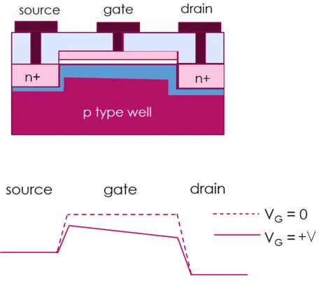
For at least three decades, the workhorse device of the semiconductor in-dustry has been the metal oxide semiconductor system, shown in Fig. 2.1. This is a three terminal device, with current flowing from source to drain controlled by bias applied to the gate. To understand the operation of the
Figure 2.1: Metal Oxide Semiconductor (MOS) transistor schematic
(top) showing source terminal connected to n+ region, gate terminal over
channel region separated by SiO2, and drain terminal connected to drain
n+ region and the associated bandstructure (below). Note how the built in
voltage described in Chapter 1, Vbi, between the source and channel, acts
to minimise electron flow from the source to the channel.
2.2. METAL OXIDE SEMICONDUCTOR (MOS) TECHNOLOGY 17
Figure 2.2: Metal Oxide Semiconductor (MOS) transistor under positive
gate bias.
flow is reduced. The source to channel barrier is first driven to flatband con-dition, and ultimately an inversion layer is formed where the channel region becomes n type (with the same absolute carrier concentration as in the p type well). This is referred to as the threshold voltage, and the transistor is now considered to be in the ON state with current flowing from source to drain. In reality, the transition from the OFF state (VGS<VTH) to the ON
state (VGS≥VTH) is not abrupt.
The carriers in the source region are described by the Boltzmann approx-imation of the Fermi probability function [27], [28] given by
f(E) =e
(Ef−E kT
)
(2.1) wheref(E) is the probability of occupancy by an electron,E is the electron energy,Ef is the Fermi energy,kis the Boltzmann constant andT is absolute
height is reduced by VGS, even before the threshold voltage is reached. This
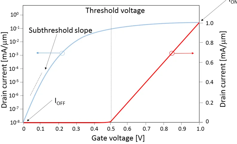
[image:39.595.157.448.321.620.2]can be seen in Fig. 2.3, where the high energy tail is clearly higher in energy than the barrier. Electrons in this high energy tail give rise to a leakage current preventing an abrupt switching characteristic. Fig. 2.4 shows a plot of source drain current on a log scale against the gate voltage on a linear scale where this subthreshold current is clear. The inverse slope of this plot
Figure 2.3: Electron energy distribution function showing high energy
tail (labelled thermal tail) with energy exceeding the source - gate energy
barrier. Electrons in this high energy tail give rise to subthreshold current
2.2. METAL OXIDE SEMICONDUCTOR (MOS) TECHNOLOGY 19 in the subthreshold region is given by
( kT
q )
ln(10) =>60mV /decade (2.2) At room temperature, the slope is 60mV / decade. In other words, to reduce the source drain current by one order of magnitude, the gate voltage must be reduced by at least 60mV. Through innovation such as high permittivity gate dielectric materials and non planar fin field effect transistor devices (Fin-FETs) [29], capacitive coupling of the gate to the channel has been enhanced to reduce the subthreshold slope, but the slope is fundamentally limited to 60mV/dec. This limitation on the subthreshold slope represents a major con-straint for the industry for a number of reasons. To optimise performance, the drive current, ION, (source drain current with maximum gate signal
ap-Figure 2.4: Drain current as a function of gate voltage showing
[image:40.595.73.470.416.658.2]plied) should be maximised, and the OFF (leakage) current, IOFF, should be
minimised. Maximising ION is important as this current charges / discharges
the parasitic capacitance of the following gate(s), and thus determines the speed performance of the circuit. To turn on a transistor in a circuit, the full VDD signal is applied to the gate. Although the transistor is in the ON
state once the threshold voltage is reached, this “gate overdrive” (VDD -VTH)
increases ION as the carrier concentration in the channel increases beyond
in-version as the gate voltage is increased, leading to higher ION, see Fig. 2.4.
It might therefore be concluded that to maximise ION, the threshold voltage
should be reduced as much as possible to maximise VDD-VTH. However, for
reasons of power conservation, IOFF must be minimised. As outlined above,
the transistor does not switch off abruptly below VTH. In the best case
sce-nario, the rate of current reduction is limited to 60mV/dec. Therefore, as VTHis decreased to maximise the drive current, the leakage current increases
exponentially as shown in Fig. 2.5
2.3
CMOS - State of the Art and Challenges
2.3. CMOS - STATE OF THE ART AND CHALLENGES 21
Figure 2.5: CMOS transistor characteristic. To improve energy
perfor-mance,VDD andVT H can be scaled down, but the>60 mV/dec
subthresh-old swing causes rapid increase inIOF F.
carried by holes. This transistor is turned ON when the gate signal is low, and OFF when the gate signal is high. Conversely, the lower transistor is an NMOS device, and is turned ON when the gate signal is high, and OFF when the gate signal is low. The output from this circuit is either logic 1 (∼VDD) or logic 0 (GND), as described in Chapter 1. In the case of a
logic 1 output, the PMOS transistor is ON, thus connecting the output to VDD, whereas in the case of a logic 0 output, the NMOS transistor is ON
Figure 2.6: CMOS circuit configuration: no connection across the power
rail when circuit is stable (not switching).
2.4. NANORELAYS FOR REDUCED LEAKAGE 23 fundamental energy efficiency of the MOS transistor must be addressed if Moore’s law is to continue. This is a major issue for the industry, and it is this challenge that provides the high level motivation for the work outlined in this thesis.
2.4
Nanorelays for Reduced Leakage
A number of alternative devices that do not rely on thermionic emission have been suggested to address the power efficiency crisis of MOS transis-tors. One such candidate is Tunnelling Field Effect Transistors (TFETs), where current flow is based on tunnelling of carriers through a barrier rather than thermionic emission over a barrier. The switching mechanism is based on modulating the ability of the carriers to tunnel through to the channel, and subthreshold slopes of less than 60mV/dec have been demonstrated by Ionescu et al [32], for example. However, these transistors are hampered by limited ION current, with implications for circuit speed as noted above. The
Figure 2.7: (a) A nanorelay with a suspended beam of length L, and
thicknesst, separated by an air gapg, from the substrate. Note the dimple
at the end of the beam which gives a reduced separation of gd. (b) A bias
applied between the beam (Drain) and Gate terminals causes the
capaci-tor comprising the beam and gate with air dielectric, to charge up. The
electrostatic force then causes the beam to bend bringing the Drain in to
contact with the Source at the dimple contact.
the neutral position, thus turning the switch OFF, when the gate bias is re-moved. This switching mechanism is abrupt, thus avoiding the subthreshold leakage of MOS devices. Furthermore there is an air gap between the source and drain, minimising gate leakage in the OFF state.
2.5. THESIS OVERVIEW 25 problems. The electrostatic force available to pull the active element (can-tilever beam) in to contact with the source scales with the active device area. Further, the requirement to operate at CMOS compatible voltage (∼1V) lim-its the force, and this problem is exacerbated by the inverse beam stiffness dependence on length, as will be shown in Chapter 3. On the other hand, once the switch is in the closed position, stiction forces which are known to dominate at the nanoscale, must be overcome to allow the beam to be restored to the neutral position when the gate voltage is removed. Contrary to the case for low voltage operation, this requires that the beam be suffi-ciently stiff. The nature of the contact interface is also critical. In addition to the mechanical properties just discussed, the contact must be capable of carrying sufficient current, and must withstand repetitive impact without significant wear. For example in [34], Peschott et al point out that to guar-antee functionality for ten years based on 100MHz operating frequency with a duty factor of 1%, the device must withstand 3x10¹⁴ ON / OFF switching cycles. In Chapter 5, it is shown that for this operating frequency, a current of 100nA per nanorelay is required in a typical circuit configuration.
2.5
Thesis Overview
Chapter 4 begins with a review of cantilever beam nechanics. The stiffness of theoretical beams is described, and the need to build and validate models of the stiffness of these beams is addressed. This is followed by a description of the fabrication of arrays of nanoscale cantilever beams. The dimensions of these beams are varied in a systematic and controlled manner. The stiffness of these beams is then measured using force spectroscopy in an atomic force microscope (AFM). This technique is described in detail, along with the results from the fabricated array. The need for validated analytical and finite element models to accurately predict the mechanical behaviour of these nanoscale beams is then presented, and the model results are compared to the results of experimentally measured fabricated nanoscale beam arrays. The models are modified to account for practical nonidealities found in the fabricated beams.
In Chapter 5, the objective of intercepting the industry roadmap at the 22nm node is discussed. Taking this technology node as a basis, reasonable dimensions for a cantilever beam device are determined, and this leads to adhesion force requirements, while electrical specifications are derived from practical circuit implementations. Using an AFM tip and substrate to repli-cate the dimple and source of a nanorelay, it is possible to measure the adhesion performance of a range of material combinations by performing force -displacement measurements and measuring the adhesion force. By applying electrical bias across the tip - substrate contact, the electrical performance of various dimple - source contact materials can be simultaneously tested. These results are then compared to the aforementioned specification to de-termine if the particular candidate materials support nanorelay operation.
2.5. THESIS OVERVIEW 27 are reviewed. Preliminary experimental work demonstrating the elimination of stiction is presented as a potential route to reliable device operation.
Chapter 3
Theory
3.1
Mechanics of Cantilever Beam
Nanore-lays
Consider the cantilever beam nanorelay design shown in Fig. 3.1. The device is based on a cantilever beam which acts as the active element. A bias is applied to the gate terminal, which, together with the cantilever beam, acts as a capacitor. The electrostatic force arising from the charge on this capacitor causes the cantilever to accelerate towards an opposing source contact, thus closing the switch. Note the contact dimple on the end of the cantilever, which defines the contact interface, and reduces switching time by minimising beam travel. As the gate voltage is reduced, the combination of electrostatic force and van der Waals (vdW) force ensures the switch remains in the closed position until the pull-out or release voltage is reached, at which point, the beam spring restoring force overcomes these forces, and the beam moves back to the neutral position. The device can also be designed to remain in the closed position when the gate voltage is removed, allowing nonvolatile
Figure 3.1: Schematic of cantilever beam nanorelay device. The
electro-static force between the actuation beam and the gate arising from the gate
voltage, causes the device to switch to the ON state.
memory functionality. The dimple gap, gd, is a key design parameter which
determines whether or not the device will display this hysteretic behaviour as explained below. Note that the mechanical spring restoring force acting on the beam is a linear function of displacement,
F =−kz=−k(g0−g) (3.1)
where F is the applied force, k is the stiffness and z is the displacement or distance the beam has travelled towards the opposing contact, g0 is the as
fabricated actuation gap thickness and g is the actual gap thickness. By modelling the beam and gate electrode as a parallel plate capacitor of ca-pacitance, C, it can be seen that the electrostatic force experienced by the cantilever, on the other hand, is a superlinear function of displacement,
Felec = (
1 2)qE =
1 2 ( CV2 g ) = 1 2 ( ϵ0W L
g ) (
V2 g
)
= ϵ0W LV
2
2g2 (3.2)
whereqis the electronic charge,E is the electric field,W andLare the width and length of the beam, V is the applied voltage and g is the actuation gap distance. At equilibrium, the electrostatic force is balanced by the spring restoring force.
k(g0−g) =
ϵ0W LV2
3.1. MECHANICS OF CANTILEVER BEAM NANORELAYS 31 As the displacement of the beam from the neutral position increases due to the applied gate voltage, there comes a point where the electrostatic force will be unconditionally larger than the spring restoring force. At this point, the beam will abruptly jump to contact. This phenomenon, described by Rebeiz [35], is known as “pull-in”, and Kaajakari [36] has shown that this critical displacement occurs when the beam has moved by g0
3. This phenomenon occurs at the pull-in voltage given by Yaung [37] as
Vpi =
√( 8 27 ) ( kg3 0 ϵ0(W L)
)
(3.4)
As noted above, nanorelays frequently utilise a contact dimple which can be seen in Fig. 3.1, where the dimple gap, gd, is shown. This dimple
defines the patterned contact area and can be designed independently of the as fabricated actuation gap. If the dimple gap is less than g0
3, then the pull-in phenomenon will not occur, because the dimple will contact the source electrode before the beam displacement reaches g0
3. The mode of operation (whether pull-in or non pull-in) has implications for the device operating characteristic. For a device operating in pull-in mode (gd > 13g0),
the actuation gap, which reduces to g0 − gd on contact, leaves the beam
closer to the gate electrode, so the electrostatic force is larger for the same
Vpi. To release the beam, the voltage must be reduced below Vpi leading
Figure 3.2: Mechanical restoring force (Fk) and electrostatic force (Fe)
for (a) a pull-in mode nanorelay and (b) a non pull-in mode nanorelay.
When operating in pull-in mode, the beam is closer to the gate electrode
when the device is ON (labelled g0-gd on the Z axis), leading to higher
electrostatic force. The net downward force (Fe-Fk) holds the beam in the
contact position until the electrostatic force is reduced below the restoring
force by reducing the gate voltage. This gives rise to the hysteresis visible
in Fig. 3.3. In the non pull-in mode device, the net force (Fe-Fk) is zero
when in the contact position (again labelled g0-gd on the Z axis), and the
beam returns to neutral position as soon as the gate voltage is reduced,
neglecting adhesion force (adapted from [37]).
In the case of the pull-in mode device, the electrostatic force (solid line) is greater than the linear force (dashed line) when the relay is ON. In order to turn the device OFF the gate voltage must be reduced below Vpi to reduce
3.1. MECHANICS OF CANTILEVER BEAM NANORELAYS 33
Figure 3.3: Nanorelay hysteretic operation: the nanorelay turns on at
VPI but does not turn off until the gate voltage is reduced to VPO
force but balances the spring restoring force when the device is turned ON. Thus the spring restoring force immediately overcomes the electrostatic force as the gate voltage is reduced fromVpi. When a relay operating in non pull-in
mode (gd < 13g0) turns ON, the actual gap, g, is given by g0−gd, and the
turn on voltage (denoted Vpi by convention) is given by
Vpi=
√
2kef fgd(g0−gd)2
ϵ0Aef f
(3.5) where kef f is the effective spring constant of the actuation beam, and Aef f
is the overlap area between the actuation beam and the fixed gate electrode. When contact is established, the force is described by
ϵ0(W L)2
2g2 +Fadh =k(g0−g) (3.6)
where Fadh is the surface adhesion force. At the release point where g =
g0−gd, the release voltage is given by
Vrl =
√
2(kef fgd−Fadh)(g0−gd)2
ϵ0Aef f
where Aef f is the overlap area between the actuation beam and the gate
electrode.
3.2
NEMS Devices: State of the Art
As described by White in [39], mechanical switches have been candidates for computing going back to the 1930s. However, for the past thirty years, CMOS technology has been dominant. This dominance was the result of the energy efficiency of CMOS (compared to TTL for example as described in Chapter 1). As devices have been scaled to the nano regime, this advantage has been eroded. As explained in Chapter 2, the device supply voltage, VDD,
and the threshold voltage, VTH, should be reduced to minimise power
3.2. NEMS DEVICES: STATE OF THE ART 35
Figure 3.4: Scaling of multi terminal relay device. The device evolved
from a 90µm four terminal device to a 15µm six terminal device with
mul-tiple source (S) and drain (D) contacts for additional functionality. To
switch the device, a control voltage is applied between the gate (G) and
body (B) terminals [40].
make contacts on (multiple) source and drain contacts. While this device is micron sized, the device has been scaled from 90µm to 15µm as can be seen in Fig. 3.4, and has been refined to reduce its footprint and increase the number of contacts to allow complex functional logic to be implemented. The CB devices, meanwhile, utilise a variety of materials including single crystal Si, polysilicon, CNTs and various metals, but all typically feature micron dimensions, and feature Vpi in excess of 1V. Metal contact dimples such as
showed how a device based on Al / TiN / W in the back end could deliver a subthreshold slope of 5mV/dec with an ION/IOFF ratio of 103 (a state of the
art MOS device would achieve a ratio of 106).
However, challenges remain. In order to achieve low switching voltages compatible with CMOS technology, beams tend to be long (several µm). This arises from the difficulty of patterning very small actuation gaps (ideally 10nm or less) and the constraints imposed on gap dimensions by the design rules for the particular technology. In [46], Leeet al proposed a novel design to address this issue based on a novel pipe clip structure to achieve a 4nm thick air gap. More generally, for the larger gaps typically used, the beam stiffness (which is inversely proportional toL3) must be reduced.
While metal contacts provide good electrical behaviour, the metallic bond-ing, and the associated large van der Waals forces, can be problematic for non volatile operation, given their adhesive nature. Even when stiction can be overcome, reliability remains as a major challenge. The actual contact area is less than the physically patterned contact area, with the actual contact area dominated by contacts via asperities. The current density at these asperities is high enough to cause microwelding and contact ablation. Unlike radio fre-quency (RF) applications of microelectromechanical systems (MEMS) relays, where contact resistance must be low to minimise insertion losses (i.e. loss of signal power from the resistance of a component inserted in the circuit), a relatively high contact resistance (e.g. 10KΩ) can be tolerated in NEMS applications. This is because the electrical (RC) delay of a nanorelay (∼ps) is about a thousand times shorter than the mechanical delay (∼ns) arising from the travel time associated with beam displacement. With this in mind, it has been shown that a dielectric material such as TiO2 can be used to
3.2. NEMS DEVICES: STATE OF THE ART 37 increased electrical time constant (RC delay) remains well below the mechan-ical time constant. A further advantage of this approach is that oxidation of the metal contact can be avoided (for Ru, however, Lee et al points out that RuO2 is conducting and so less problematic [47]).
Akarvardar et al [48] benchmarked several metals against Si as the beam material. A model was presented that showed that by using a low density 225nm Si beam, 1V operation would be feasible with single crystal Si, but this has not been experimentally verified. Single crystal beams (both cantilever and double clamped) are quite common in resonator applications [49], [50], [51], but beam lengths are in the micron range. The low mass and high resonance frequencies of such suspended Si nanobeams lend these devices to applications in high resolution mass sensing. While the beam lengths are greater than 1µm, their integration with CMOS signal processing circuitry reflects the promise for wider application of suspended Si NEMS devices for other applications such as digital logic and power gating. In addition to submicron Si beams, a number of avenues have been explored to address the relatively high pull-in voltage required for devices in the literature. The use of a fourth “body” terminal is shown in Fig. 3.5 for a crab like relay device [38]. This idea is similar to a floating bias terminal proposed by Yanget alfor MEMS [52]. By applying bias to the body terminal, the switching voltage, Vgb, can be reduced below 1V. Jeon et al [53], has shown that by judicious
Figure 3.5: Schematic of four terminal relay. Device operation is based
on the electrostatic force arising from the voltage between the gate and the
fourth “body” terminal [38].
leading to an operating voltage of 400mV. Fig. 3.6 shows the novel pipe clip structure achieved using high density plasma (HDP) deposition [54] over a self aligned trench to realise the 4nm gap.
Figure 3.6: Schematic of two terminal NEM switch. The expanded image
shows how the 4nm gap is realised through the use of a pipe clip structure
3.2. NEMS DEVICES: STATE OF THE ART 39 As the mechanical requirements of the beam (sufficiently stiff to overcome contact adhesion force, with a low adhesion dimple contact surface) and the electrical current carrying requirement can sometimes be contradictory, a number of designs seek to decouple these requirements. For example, Parsa
et al [55] [56] [57], use a compliant polySi beam to define the mechanical performance with a Pt coated beam providing electrical contact. To prevent secondary pull-in, where the active element (beam) causes a short between the source and gate, see Fig. 3.7, the cantilever is modified in the actuation area to provide a non compliant stiffness. In [58], Leeet aluse a dual sidewall coating on the beam consisting of HfO2, which provides electrical isolation
between the drain and the beam and Pt which provides electrical contact between the source and drain terminals, as shown in Fig. 3.8. This adds
Figure 3.7: Cantilever beam (CB) device with the beam modified to be
Figure 3.8: CB device with HfO2 / Pt coating on beam. The HfO2
isolates the drain from the beam, and Pt provides electrical contact between
the drain and source providing the ability to mimic both PMOS and NMOS
behaviour. The arrangement also allows independent biasing of the beam
[58].
3.2. NEMS DEVICES: STATE OF THE ART 41
Figure 3.9: This device achieves reduced voltage operation by increasing
the electrostatic force with a large area (∼2x4µm) capacitive paddle, as
3.3
Circuits incorporating NEMS: State of
the Art
Due to the relatively long switching time of a NEMS device, associated with mechanical displacement of the active element, it is best to design nanorelay based circuitry to avoid sequential device switching, thereby exploiting the energy efficiency of these devices while mitigating their limited speed. In this way, complex logic circuitry can be configured where all relays switch si-multaneously through circuit design tailored to NEMS device characteristics, thus limiting the delay to one mechanical switching period, while simultane-ously exploiting the aforementioned leakage and subthreshold characteristics to drive energy efficiency.
3.3. CIRCUITS INCORPORATING NEMS: STATE OF THE ART 43 reliability problems to be overcome (high ON resistance, RON, and gradual
switching transition compared to the abrupt switching of the isolated NEM device), the work demonstrated the potential for integration.
By switching from planar to out of plane (vertical geometry), the transis-tor interconnect wiring can be used to integrate NEMS with CMOS. State of the art CMOS integrated circuits published by Intel [13] feature 12 layers of interconnect wiring. Xu et al [62] and Mu˜noz-Gamarra et al [41] showed that the aggressive scaling of interconnect layers can be exploited to incor-porate vertical cantilever beam devices in a monolithic integration strategy. An example is shown in Fig. 3.10. It is projected that 1V operation with a switching time of 20ns is feasible, and that by using the vertical out of plane orientation, a footprint of 0.1 µm2 is possible. Circuit simulations utilising such devices have been performed for various functions. For example, Xuet al [62] show how energy efficiency can be improved by integrating this NEM device in CMOS buffer circuits, or in power gating, where a non-volatile NEM device based circuit can be used to power off inactive logic blocks in an energy efficient manner. Other proposed circuits which could benefit from cointegration of NEMS and CMOS include field programmable gate arrays (FPGA) [63], static random access memory (SRAM) [64] and header / footer switches [65].
Taking SRAM as an example, Bota et al [66] analyse the performance of NEM relays designed using 65nm node technology in a conventional SRAM cell. The nanorelay is a CB device utilising one of the metal layers with a 17µm long, 100nm wide, 220nm thick beam with an as fabricated source gate gap of 100nm and stiffness of 8.4 x 10⁻²N/m. Using this device, they develop
Figure 3.10: Vertically oriented cantilever beam (CB) device
imple-mented in the back end of line (BEOL) of an integrated circuit. The
in-put node connects to the actuation beam located between two actuation
electrodes. Depending on the input signal, the beam is electrostatically
at-tracted to one of the actuation electrodes thus connecting one of the data
terminals (D0 or D1) to the output [62].
position, and 0.26 aF with the device in the OFF position. The switching time, τmech, is 361ns, and the ON resistance of the device is 1KΩ. This
nanorelay is used in various configurations in the 6T SRAM cell in circuit simulations, and the impact on circuit performance is determined. They find that the leakage power can be reduced by up to 78%. Interestingly, the long switching time of the relay does not impact on the read or write time of the circuit (although a latency delay equal toτmechis incurred). In addition, the
3.3. CIRCUITS INCORPORATING NEMS: STATE OF THE ART 45 to improve the static noise margin of the circuit.
More complex MEM relay based circuits have also been demonstrated. For example, Fariborzi et al demonstrate a compressor circuit built using 46 scaled MEM relays in [67]. The demonstrator chip shown in Fig. 3.11 contains relay based logic gates, oscillators and memory. This shows great promise if the scaling challenge can be overcome [68].
[image:66.595.128.411.382.657.2]In addition to logic and memory applications, NEMS are also used as sensors [69], for example in mass detection, where they offer unprecedented resolution. The integration of these NEMS sensors with CMOS reflects the state of the art as it relates to the integration of NEMS devices in CMOS
Figure 3.11: Die photo with the relay based logic, oscillator and memory
3.4. NEMS / NANORELAY TECHNOLOGY: CHALLENGES 47
3.4
NEMS / Nanorelay Technology:
Chal-lenges
3.4.1
Miniaturisation
There are two types of nanorelay employed in CMOS circuitry in the litera-ture. The crab like multi-terminal relay developed by Kamet al at Berkeley [40], and simpler cantilever based devices such as that published by Liuet al
3.4.2
Adhesion
In the CB nanorelay shown in Fig. 3.1, there are multiple forces acting on the active element. The applied voltage to the gate electrode gives rise to an electrostatic force which acts to “pull-in” the active element towards the source electrode. The dynamics of this motion is described by the equation
Felec =m
d2x dt2 +b
dx
dt +kx (3.8)
where m is the mass, x is the displacement, b is the damping coefficient caused by displacement of air molecules and anchor losses, andk is the beam stiffness [74]. The electrostatic force arises from the capacitive charging of the beam with respect to the substrate. As noted earlier, (cf. Eqn. 3.2), this capacitance is given by
C = ϵ0(W L)
d (3.9)
and the force (F = qE) acting one of the capacitor plates (the movable beam) is then given by
F = ϵ0(W L)V
2
2d2 (3.10)
The spring restoring force of the beam, which balances this electrostatic force, is linear
F =−kx (3.11)
3.4. NEMS / NANORELAY TECHNOLOGY: CHALLENGES 49 voltage at which this condition is met is given by
Vpi =
√(
8 27
) ( kg3
0 ϵ0(W L)
)
(3.12) with the terms described earlier in Section 3.1. As the gate voltage is now reduced back to zero, an additional force associated with the interface must be considered. At the nanoscale, it is known that adhesive forces, which scale with surface to volume ratio, become important as described by Ra-makrishnaet al [75] and Gauthier et al [76]. Because of this adhesion force,
Fadh, the beam remains in the closed position even after the gate voltage
falls below the pull-in voltage. This gives rise to the hysteretic device char-acteristic shown in Fig. 3.12. However, if the spring restoring force of the beam does not exceedFadh, the beam will remain permanently in the closed
position. Thus Fadh places a minimum bound on the CB stiffness, and thus,
the operating voltage. For this reason the adhesion force is critical. The adhesion force arises from van der Waals interactions, electron exchange
in-Figure 3.12: NEM operating characteristic: note the abrupt switching
teractions, unsaturated bonds and capillary effects. The van der Waals forces arise from permanent and instantaneous polarization of atoms, and comprise dipole-dipole force, dipole - induced dipole force and dispersion forces (charge fluctuation). These will be described in detail in Section 6.5. As described by Israelachvili in [77], the adhesive force can be expressed as
Fadh,v =
HAc
6π(D+D0))
3 (3.13)
whereH is the Hamaker constant of the contact materials and Acis the real
area of contact (i.e. actual contact dominated by asperities rather than the physically patterned electrode area), D is the separation and D0=0.165nm is an effective cutoff distance in this continuum approximation from [78]. To minimise contact resistance, metallic contacts might be used. However, this presents an adhesion problem. These contacts usually feature strong adhe-sion, arising from a strong electron exchange interaction which dominates the vdW force. An estimation of this force is given by
Fadh,m =−2γAc
d dD
([
1− D−D0
λM
] e−
(D−D0) λM
)
(3.14) where γ and λM are the surface energy and electron mean free path
re-spectively [77]. To address this adhesion problem, metal contacts have been coated with a thin layer of TiO2 [40], for example, or implemented using
rhuthenium, Ru, [42] which oxidises to form conducting RuO2. It should be
noted that the mechanical delay, τmech, is about three orders of magnitude
greater than the electrical RC time constant,τelec, and so there is some
mar-gin for increasing the resistance (and thusτelec throughRC) before impacting
3.4. NEMS / NANORELAY TECHNOLOGY: CHALLENGES 51 Capillary forces also add to adhesion, and can be difficult to avoid if operating in ambient conditions. For Si, approaches such as hydrogen termi-nation or passivating Si with fluorine can reduce the effects of unsaturated bonds and capillary effects. This topic will be dealt with in more detail in Chapter 5 of this thesis.
3.4.3
Contact reliability
The importance of minimising adhesion for low operating voltage was ad-dressed above. Nevertheless, the contact must still be conductive with a contact resistance no greater than about 100KΩ (depending on application) according to Kam et al [40]. The scaling of relay devices towards the nano regime exacerbates this problem, as the real contact area is typically even less than the apparent contact area due to roughness, where the current is carried by a number of asperities. This means the current density can be much higher than is apparent from the nominal contact area. Furthermore, the device operates by treating the beam as one plate of a capacitor. The beam charges up (thus generating the electrostatic force), and the stored charge dissipates upon contact. This initial discharge current density can be sufficient to microweld or even ablate the contact. Similar to the problem with adhesive metal contacts, this can be mitigated by coating the metal contact with a dielectric. Kam et al [40] note that of the common dielectric materials, TiO2 reduces the conductivity least, and has the added advantage
of preventing oxidation of metallic contacts such as W. However, whatever material system is used, the repetitive impact of switching can cause degra-dation, ultimately leading to premature failure.
resistance to wear and tear simultaneously. Strelleret al [79] propose plati-mum silicide, whose properties can be tuned to achieve 150% of the hardness of as deposited Pt with a contact resistance within 10% of as deposited Pt. Mayet et al [80] demonstrated the use of amorphous WNX which is
electri-cally conductive and hard (with a hardness of 3GPa and a Young’s modulus of 300GPa) as both a structural element (the cantilever beam) and the con-tact material. The authors deposited this material using reactive sputter-ing, and patterned CB devices using electron beam lithography (EBL) and plasma etch. Device operation was demonstrated, but the authors note the requirement for further optimisation to reduce the contact resistance. The performance and reliability of both Pt and RuO2 was investigated by de Boer et al [81], who found that that RuO2 performed better than Pt which failed
due to wear after 105 switching cycles, while the RuO2 contacts survived 3 x
108 switching cycles, albeit with unstable resistance. Silicon Carbide (SiC) is
Chapter 4
Si nanocantilevers: mechanics,
fabrication & testing
4.1
Introduction
This chapter opens with a brief review of cantilever beam mechanics, and introduces an analytical expression for the stiffness of an ideal cantilever beam. The design and fabrication of an array of Si nanocantilever beams is then described, with detailed discussion of the CMOS compatible processing steps (resist coating, lithography, plasma etch, wet etch and strip) involved in their manufacture. This is followed by a description of the use of atomic force microscope (AFM) based force spectroscopy to measure stiffness. Finally experimental results are presented, and fabrication related non idealities are analysed and modelled. The applicability of the analytical model to the nanoscale is then clarified.