HASHIM, A. A., BARRATT, D. S., HASSAN, A. K.
0002-7891-8087>, EVANS-FREEMAN, J. H. and NABOK, A.
<http://orcid.org/0000-0002-9078-1757>
Available from Sheffield Hallam University Research Archive (SHURA) at:
http://shura.shu.ac.uk/980/
This document is the author deposited version. You are advised to consult the
publisher's version if you wish to cite from it.
Published version
HASHIM, A. A., BARRATT, D. S., HASSAN, A. K., EVANS-FREEMAN, J. H. and
NABOK, A. (2006). Resistivity network and structural model of the oxide cathode for
CRT application. Journal of display technology, 2 (2), 186-93.
Copyright and re-use policy
See
http://shura.shu.ac.uk/information.html
186 JOURNAL OF DISPLAY TECHNOLOGY, VOL. 2, NO. 2, JUNE 2006
Resistivity Network and Structural Model of the
Oxide Cathode for CRT Application
Abbass A. Hashim, David S. Barratt, Aseel K. Hassan, Jan H. Evans-Freeman, and Alexei V. Nabok
Abstract—In this paper, the electrical properties of oxide cathode and oxide cathode plus, supplied by LG Philips Displays, have been investigated in relation to different cathode activation regimes and methods. Oxide cathode activation treatment for different dura-tions has been investigated. The formadura-tions of the compounds as-sociated to the diffusion of reducing elements (Mg, Al, and W) to the Ni cap surface of oxide cathode were studied by a new sugges-tion method. Scanning electron microscopy (SEM) coupled with energy dispersive X-ray spectroscopy (EDX) was used as analyt-ical techniques.
Al, W, and Mg doping elements take place during heating to 1080 K (Ni-Brightness) under a rich controlled Ba–SrO atmos-phere through an acceleration life test. The chemical transport of these elements was occurred mainly by the Ni cap grain boundary mechanism with significant pile-up of Mg compounds. Al and W show a superficial concentrations and distribution.
A new structural and resistivity network model of oxide cathode plus are suggested. The new structural model shows a number of metallic and metallic oxide pathways are exist at the interface or extended through the oxide coating. The effective values of the re-sistances and the type of the equivalent circuit in the resistivity net-work model are temperature and activation time dependent.
Index Terms—Ba and Sr oxides, electrical properties, electron emission, oxide cathode.
I. INTRODUCTION
R
EDUCING the cathode coating resistivity by the incorpo-ration of a conductive metallic phase enhances the emis-sion current density. This is the main idea of the current gener-ation of oxide cathode produce by LG Philips Displays compo-nent. One of the significant advances in the last few years has involved the work of this company on the development of new compositions for the emissive layer of their oxide cathodes. The oxide cathode comprises a top layer of Ba–SrO mixed with a 5% (oxide cathode) or 2.5% (oxide cathode plus) Ni powder cermet with surface area of 0.0165 cm and layer thickness of approxi-mately m deposited onto a Nickel alloy cap [1]–[3]. This Ni cap contains low levels of W (2.98%), Mg (0.125%)andAl (0.1%) as activators in addition to small amounts of yttrium, zirconium, and iron.
Two different methods have been used to study the electrical properties and the formation of the interface layer. A special dummy tube was designed for this purpose. Numerous theories
Manuscript received January 3, 2006; revised February 10, 2006.
A. A. Hashim, A. K. Hassan, J. H. Evans-Freeman, and A. V. Nabok are with the Material and Engineering Research Institute, Centre for Electronic Devices and Materials, Sheffield Hallam University, City Campus, Sheffield S1 1WB, U.K. (e-mail: [email protected]).
D. S. Barratt is with LG Philips Displays Blackburn, Blackburn, BB1 5RZ, U.K..
[image:2.594.309.552.164.315.2]Digital Object Identifier 10.1109/JDT.2006.874506
Fig. 1. Schematic diagram of the dummy tube test and measurement circuit.
have been used for the conduction mechanisms of oxide cath-odes in terms of the electron percolation and MS junction [4].
Scanning electron microscopy (SEM) and X-ray spec-troscopy (EDX) analysis of oxide cathode samples with different treatments have been performed. SEM micrographic images give evidence that the conductivity is cathode type dependent (“S” or “N” types). EDX analysis proved that the conductivity is dependent on the amount of the Ba contaminate in the oxide layer. The analysis showed the penetration of the activators through the oxide, specifically the Al agents.
II. EXPERIMENTALDETAILS
The Loosjes and Vink procedure was applied to measure the cathodes’ conductivity [5]. The cathode assemblies were mounted, face to face in pairs in a specially designed holder inside a glass chamber under vacuum of about 3 10 mbar [6]. A set of cathodes were activated at 1425 K, 1200 K, and 1125 K for different periods of time between 1 hour and 12 hours and the two oxide layers were combined to form a single layer with thickness of approximately 120 10 m as a result of conversion and activation processes.
Another set of two cathodes were used in a new method to in-vestigate the interstitial growth of the interface layer. One of the cathode is a normal oxide coated cathode plus and the other is an uncoated cathode plus [4]. The two cathodes were assembled, face to face with an attach-contact between them. The entire as-sembly, as shown in Fig. 1, was mounted inside a dummy tube which was evacuated prior to and during the decomposition and activation process.
The dummy tube was sealed under vacuum of about 10 mbar. The filament temperature of the uncoated cathode was elevated to the accelerated temperature of 1080 K and
Fig. 2. Conductivity-temperature dependence after activating the oxide cathode (Ni 5%) to 1200 K and operated to (a) for 100 h and (b) for 200 h. (Color version available online at http://ieeexplore.ieee.org.)
operated for different lifetime up to 1896 h (real-time 14 200 h) [4].
III. RESULT ANDDISCUSSION
A. Electrical Measurement and Conduction Properties
Current-voltage characteristics of face to face cathodes in vacuum chamber were measured in the temperature range be-tween (300–1200) K [1].
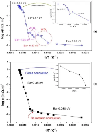
In Fig. 2(a), the dc conductivity of the 5% Ni cathode is found to be increase when sufficient oxide thickness is accelerated for 100 h in the temperature range 825 500 K [7]. This can be only understood by visualizing the WO layer to provide a duction path which is in parallel with the existing electrons con-duction paths in the oxide. The specific resistivity of WO is increased by two orders of magnitude from 10 10 , when the oxygen concentration is increased from 5% to 30% [8], [9].
This specific resistivity is also decrease in other manners like temperature elevation. This seems to have happened at the in-terface layer of hot cathodes at the acceleration temperature due to the fact that the Debye temperature of the barium oxide is quite low Ba K [10]. Therefore, the increase can be explained by the lowering of the total cathode resistance as the conductivity of WO increases by two orders of magnitude giving activation energy of eV and the system be-comes more conductive at temperature range 500 625 K [11]. This activation energy is slightly larger than 0.77 and 0.84 eV for amorphous and crystalline tungsten oxide, respectively [8].
188 JOURNAL OF DISPLAY TECHNOLOGY, VOL. 2, NO. 2, JUNE 2006
Fig. 3. Dependence of conductivity on temperature for the oxide cathodes (Ni 2.5%) assembled in a vacuum chamber and activated for ( 1125 K), (1425 K) and ( 1200 K). (Color version available online at http://ieeexplore.ieee.org.)
Approximately same activation energy value eV is observed again at the operation temperature range of (950–1050) K. This conduction can be interpreted in term of the surface conduction via Ba on BaO monolayer [6], [7]. The accumulation of the Ba as an effective layer is a result of the long operation time of this semi-closed system [7]. These adsorbed layers on the Ba–SrO grain surfaces inserted another resistance to the resistivity network of the oxide cathode. This resistance is most likely to be in parallel [1]. The effect of the Ba layers on the oxide conductivity can be viewed at low temperature range (300–600) K and high temperature range (1000–1200) K very clearly after several hundreds hours of operation, as shown in Fig. 2(b) [1]. At the high temperature range, the pores contribution was disappeared due to the effect of the Ba multi-layers contamination [13].
Fig. 3 shows the conductivity follows the resistivity network in the oxide cathodeplus (2.5% Ni powder). This network ischanged due to the equivalent circuit (series or parallel type) between the resistance contents of the oxide cathode. The effective values of these resistances and the type of the equivalent circuit are temper-ature and activation time dependent. The figure shows, precisely, that the activation of the cathode for 12 h at 1200 K results in the formation of Ba metallic pathways, which percolate through the oxide and cause a decrease in the pores conductivity contribution. This is exactly what has happened in Fig. 2(b) after accelerating the (5% powder) oxide cathode to 200 h. However, the acti-vation of the cathode for the same duration at lower temperature (1125 K) caused a conduction path which is in series with the existing electrons conduction paths (grain-grain) in the oxide. The electron is prompted to pass to the pores (electron gas) at the threshold temperature of 600 K [5].
The metallic pathways increased the conductivity about 4 or-ders of magnitude at the RT range when the activation temper-ature was elevated from 1125–1200 K, whereas the high acti-vation temperature (1425 K) shows a limited effect for the
con-taminated Ba on the oxide conductivity at the temperature range (300–450) K. It also shows a clear pores conductivity contribu-tion at high operacontribu-tion temperature (1000–1300) K.
The conductivity and the activation energy characteristics are strongly dependent on the life test condition. The conductivity of an activated (Ba,Sr)O coating is reported to be of the order of 10 cm [14], but the value for the new cermet oxide cathode plus with 2.5% Ni powder addition is increased to 10 cm at the operating temperature [15].
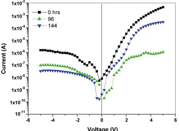
Fig. 4 shows the dc electrical characteristic which indicates very strong rectifying behavior through the M-S junction par-ticularly after 144 h lifetime inside a dummy tube test [4], [16]. The coated-uncoated cathode assembly in a dummy tube showed reversible and reproducible characteristics and showed a rectification ratio of 100. The ideality factor was calculated to gives a consistent value of about [4]. The higher value of ascribed to the tunnelling in the junction area as a result of the increasing in the electron space charge (thermionic emission) and the increasing in the Schottky effect [17], [18]. This approves the formation of the interface layer in between the oxide coating and the Ni cap. The interface layer thickness grows to 6 m after accelerating the cathode to 1896 h (real time 14 200 h) [4]. The 6- m value seems to be an effective thick-ness which may increase the reduction reaction area between the Ni surface cap activators and the oxide grains. Such a high value of the interface layer thickness indicates a nonuniform shape of interfacial layer. However, it may also prove that the interface layer grows inside the Ni cap grain boundaries and penetrates in between oxide grains [4], [19]. It may be explained in term of the influence of the interface layer in the pores space between the grain boundaries, as shown in Fig. 5.
B. Morphological and Elemental Analysis
Fig. 4. Current-voltage characteristics of cathode assembly at different acceleration lifetimes in a dummy tube test. (Color version available online at http:// ieeexplore.ieee.org.)
Fig. 5. Nonuniform interfacial layer. (Color version available online at http:// ieeexplore.ieee.org.)
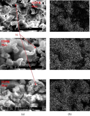
compression between the two attached cathodes and a very high temperature) is most likely to be an “S” type cathode [1]. This cathode always has low emission, and the oxide particles are considered to be sintered and have short grain-to-grain bound-aries, and the very low contact potential barrier [11]. It can be assumed that the semiconductor-type conduction through the grains will be predominant in the “S” type cathode [11]. The morphological analysis shows that the oxide became more sin-tered, the grain size increased from approximately 6 m to 10 m after twelve hours of activation at 1200 K activation tem-perature. It is also apparent that the porosity decreased with the increasing of the activation time.
In such case, the EDX analysis for the Ni cap surface shows that tungsten was the first element to diffuse through the Ni boundary grains, forming one of the tungsten oxide composi-tions [15]. The presence of Al was observed in an appreciable quantity after 3 h of activation at 1200 K. The decrease in the Al on the Ni cap surface is followed the cathode activation for more than two hours at 1425 K. This observation indicates that the Al left the interface and transported through the oxide layer. Fig. 6 shows the Al proportion quantities on the Ni cap for dif-ferent period of activation time and temperature. Obviously, for
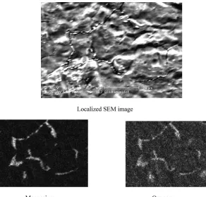
[image:5.594.39.289.324.458.2]the time period of 4–12 h at the activation temperatures 1125 and 1200 K, the Al proportion values are most likely to be temper-ature independent. The reality is that the Al diffusion depended on temperature and time when the cathode activated to 1425 K. The behavior may be taken as a strong evidence of the perco-lation of the Al through the oxide. These atoms can reduce the oxygen from the oxide grains directly and causes a Ba adsorp-tion layer on the grain surface. The evidence for this descripadsorp-tion is the Al element which was found to be distributed on the sur-face of the oxide layer [15], [20], [21].
Fig. 7, shows the SEM elementary mapping for the Al dis-tributed on the Ba–SrO surface at different period of time and activation temperature. The focusing in this figure shows that the aluminum oxide concentrated in some bright points. It can be interpreted depend on Dearnaley filament theory [10], where the Al follows the oxygen filament ended in the Ni cap surface to the top of the oxide material.
fter a long time of activation of about 12 h at 1200 K. These particles are believed to remain in their respective oxide forms (e.g., Al O for Al and MgO for Mg) distributed on the surface of the cap, concentrated in the Ni grain boundaries. Mg may also be present in the MgAl O form [19].
The sintering ratio, the oxide grain size, and the pores density are activation temperature dependent, as clearly shown in Fig. 7. The grouping ratio (oxide grains grouped together) in the oxide material activated at 1425 K is more than the sintering ratio. The figure shows also the differences in the coarsening of the Ni additives phase between the Ba/SrO grains due to the activation temperature.
2) Cathode Activated in a Dummy Tube: The dummy tube morphological analysis shows the following:
• X-ray spectrum indicates some Al and Zr elements are dif-fused on the surface of the oxide.
190 JOURNAL OF DISPLAY TECHNOLOGY, VOL. 2, NO. 2, JUNE 2006
Fig. 6. Al activator element EDX analysis distributed on the Ni cap surface through period of time and activation in a vacuum chamber test. (Color version available online at http://ieeexplore.ieee.org.)
[image:6.594.153.451.344.726.2]Fig. 8. SEM micrography for choosing area magnified for 3000 times on the uncoated Ni cap surface (cathode activated in a dummy tube and accelerated for zero hours).
These results can be accepted if it is supposed that the Mg was initially diffused to the surface then transported through the oxide quickly but with a very short path. This is explained the disappearance of the Mg from the Ni cap surface images and EDX test (Section III-B-1).
C. New Structural Model
By highlighting some points from the previous literature re-sults, using the conclusions above, it help to build a new network model for the new generation of oxide cathode. The highlighted points can be summarized as follows.
• According to the Loojese and Vink experiments in the oxide coating, there is a dependence on temperature given by [5]
(1)
where is the oxide activation energy, , the pore ac-tivation energy and , the metallic pathway activation energy.
If these mechanisms are connected parallel to each other the resultant conductivity will be at every temperature de-termined mainly by the mechanism with the highest con-ductivity. The resultant conductivity is in that case, the sum of the conductivities of the separate mechanisms.
• In oxide-coated cathodes, Dearnaley proposed that the presence of reducing agents at the activation temperature results in the removal of some oxygen from the coating [10]. At certain favorable points on the metal-oxide inter-face the oxygen may locally become conducting, perhaps
owing to an aggregation of oxygen vacancies, which may occur particularly at grain boundaries in the poly-crystalline structure. If an electric field is applied during activation the filament will then tend to grow through the oxide coating.
The far heavier barium atoms are remaining relatively undis-turbed. In the conducting chain created by a high concentration of oxygen vacancies and terminating at the metal base, the ap-plied field will cause a very large electric stress at the other end, extending as it does into the insulating oxide. Under such a stress, and at the activation temperature, Dearnaley supposed that further oxygen vacancies migrate to this tip and cause it to grow until the chain penetrates the oxide layer. The increased conductivity of the layer will eventually reduce the electric field and filament growth will come to an end [10].
The conclusion taken from the experimental results covered by these specific theories may lead to a dependent model, which is build up in the structure of the oxide cathode through the activation and operation process (acceleration). By the effect of the electrical field, the free oxygen formed a filament chain percolated in the oxide layer and ended at the Ni cap surface and oxide top layer.
cre-192 JOURNAL OF DISPLAY TECHNOLOGY, VOL. 2, NO. 2, JUNE 2006
Fig. 9. Oxide cathode new structural model taking into account all possible chemical reactions. (Color version available online at http://ieeexplore.ieee.org.)
ating conduction or emission electron and an adsorbed mono-layer or multimono-layer of Ba.
All these processes form thermal resistances which are con-nected with each other in a complicated way. It is believed that the conductivity changes occurring during the activation process can be attributed to this structural rearrangement. The coars-ening of the Ni phase between the Ba–SrO grains and in between these activator oxides make a short pathway for the electron to transport in between. The electron follows the lower resistance and reduces the number of continuous electronic pathways.
Fig. 9 shows this new model taking into account all these processes which were shown in the experimental results of this study. This model shows a number of metallic and metallic oxide pathways are exist at the interface or extended through the oxide coating. The experimental results proved few facts which can be summarized as follows.
1) Aluminum and zirconium oxide filaments have started from few microns inside the Ni cap grain boundaries [22] and percolated the oxide coating reaching the top surface. 2) Tungsten and magnesium oxides filaments have also started from few microns inside the Ni cap [22] and per-colated the oxide coating with short pathways. We have no idea how many microns are these filaments long. 3) The mono or multilayers containing free Ba and Ni
coars-ening powder provided the lowest resistivities pathways which may act as conductive links between the grains of the main oxide material.
IV. CONCLUSION
The resistivity network of the oxide cathode and the structure are affected by the oxide coating and Ni cap contents, which
are changed due to number of factors. The most important fac-tors are activation temperature, operation, or acceleration tem-perature and time. These factors are controlled by the activa-tors (Al, W, .) movement and distribution through the oxide coating and leads to changed the resistivity network or conduc-tivity pathways map of oxide coating.
The experimental result indicates that the Al left the interface and transported through the oxide layer and aluminum oxide concentrated in some bright points on the top surface of the oxide cathode. This observation was interpreted depend on Dearnaley filament theory, where the Al follows the oxygen filament ended inside the Ni cap to the top of the oxide material. This novel phenomenon was proved by the X-ray spectrum, which indicates some Al and Zr elements are diffused on the surface of the oxide. The Mg is initially diffused to the surface then transport through the oxide quickly but with a very short path and this seems has happened with the other elements like tungsten.
These activators reduces the oxygen from the oxide grains directly causing a Ba adsorption layer on the Ba–SrO grain sur-face, and inserts another resistance to the resistivity network of the oxide cathode. All these filaments were taken into account to build a new oxide cathode structural model. This model jus-tifies the main concept of this work.
REFERENCES
[1] A. A. Hashim, D. S. Barratt, A. K. Ray, and A. K. Hassan, “The study of the effect of Ba coverage through the accelerations lifetime of activated BaO/SrO cathodes,”App. Surf. Sci., vol. 243, pp. 421–428, 2005. [2] A. N. H. Al-Ajili, S. N. B. Hodgson, A. P. Baker, A. K. Ray, J. R.
[3] S. N. B. Hodgson, A. P. Baker, C. J. Goodhand, P. A. M. van der Heide, T. Lee, A. K. Ray, and A. N. H. Al-Ajili, “Processing and performance of a novel cathode material,”Appl. Surf. Sci., vol. 146, pp. 79–83, 1999. [4] A. A. Hashim, D. S. Barratt, A. K. Hassan, and A. Nabok, “Electron conduction associated with the chemical transport of reducing elements in oxide cathode for CRT’s application,”Appl. Surf. Sci., in press. [5] R. Loosjes and H. J. Vink, “The conduction mechanism in
oxide-coating cathode,”Philips Res. Rep., vol. 4, p. 449, 1949. [6] A. N. H. Al-Ajili, A. K. Ray, J. R. Travis, S. N. B. Hodgson, A. P.
Baker, and C. J. Goodhand, “Thermal decomposition and electrical conductivity of oxide cathode emission materials,”J Mater. Sci.: Mate. Elect., vol. 11, pp. 489–495, 2000.
[7] A. A. Hashim, D. S. Barratt, A. K. Hassan, and A. Nabok, “Accelerated life AC conductivity measurements of CRT oxide cathodes,”Appl. Surf. Sci., in press.
[8] A. A. Akl, H. Kamal, and K. Abdel-Hady, “Characterization of tung-sten oxide films of different crystallinity prepared by RF sputtering,”
Phys. B: Condens. Matter, vol. 325, pp. 65–75, 2003.
[9] M. Gillet, C. Lemire, E. Gillet, and K. Aguir, “The role of surface oxygen vacancies upon WO conductivity,”Surf. Sci., vol. 532–535, pp. 519–525, Jun. 2003.
[10] G. Dearnaley, “A theory of oxide-coated cathode,”Thin Solid Films, vol. 3, pp. 161–???, MONTH??? 1969.
[11] S.-I. Narita, “Relationship between thermionic emission and electrical conductivity of oxide-coated cathodes,” J. Phys. Soc., vol. 8, pp. 331–338, 1953.
[12] H. Nakai, J. Shinohara, T. Sassa, and Y. Ikegami, “Surface mor-phology and resistivity of aluminum oxide films prepared by plasma CVD combined with ion beam irradiation,”Nucl. Instrum. Methods in Physics Res. B: Beam Interaction With Materials and Atoms, vol. 121, pp. 125–128, 1997.
[13] T. N. Chin, R. W. Cohan, and M. D. Coutts, “Electronic processes in oxide cathodes,”RCA Rev., vol. 35, pp. 520–540, 1974.
[14] G. Gartner, P. Janiel, and D. Raasch, “Direct determination of electrical conductivity of oxide cathodes,”Appl. Surf. Sci., vol. 201, no. 1–4, pp. 35–40, 2002.
[15] A. A. Hashim, D. S. Barratt, A. K. Ray, and A. K. Hassan, “Formation of an interface layer in thermionic oxide cathodes for CRT applica-tions,”J. Phys. D: Appl. Phys., vol. 37, pp. 2932–2937, 2004. [16] J. M. Shah, Y.-L. Li, T. Gessmann, and E. F. Schubert, “Experimental
analysis and theoretical model for anomalously high ideality factors
(n 2:0)in AlGaN/GaN p-n junction diodes,”J. Appl. Phys., vol. 94, pp. 2627–2630, 2003.
[17] S. K. Mandal, A. B. Maity, J. Dutta, R. Pal, S. Chaudhuri, and A. K. Pal, “Au/CdS schottky diode fabricated with nanocrystalline CdS layer,”
Phys. Stat. Sol. (a), vol. 163, pp. 433–443, 1997.
[18] F. Buda, J. Kohanof, and M. Parrinello, “Optical properties of porous silicon: a first-principles study,”Phys. Rev. Lett., vol. 69, pp. 1272–1275, 1992.
[19] J. M. Roquais, F. Poret, R. le Doze, P. Dufour, and A. Steinbrunn, “Ini-tial chemical transport of reducing elements and chemical reactions in oxide cathode base metal,”Appl. Surf. Sci., vol. 201, pp. 85–95, 2002. [20] S. N. Jenkins, D. K. Barber, M. J. Whiting, and M. A. Baker, “Pre-liminary results on the chemical characterization of the cathode nickel emissive layer interface in oxide cathodes,”Appl. Surf. Sci., vol. 215, pp. 78–86, 2003.
[21] A. A. Hashim, D. S. Barratt, A. K. Hassan, and A. Nabok, “Activation process-dependent characteristics of novel thermionic oxide cathodes for CRT application,”J. Display Technol., vol. 2, no. 1, pp. 91–97, Mar. 2006.
[22] D. K. Barber, S. N. Jenkins, M. J. Whiting, and M. A. Baker, “Analyt-ical interfacial studies of double carbonate thermionic oxide cathodes over accelerated operational life,”Appl. Surf. Sci., vol. 251, pp. 42–49, 2005.
Abbass A. Hashimreceived the B.Sc. and M.Sc. degrees in solid state physics from Basra University, Basra, Iraq, in 1984 and 1989, respectively, and the Ph.D. degree from Sheffield Hallam University, Sheffield, U.K., in 2005.
He joined the oxide cathode LG. Philips research group, Blackburn, U.K., in November 2001. At present, he is a visiting researcher in the Centre of Electronics and Materials Devices, Materials and Electronics Research Institute at Sheffield Hallam University, Sheffield, UK. His main research in-terests are in thin film technologies, dielectric and semiconductor materials, nanotechnology, physical properties of polymers and electronic sensors.
David S. Barrattreceived the B.Sc. and Ph.D. de-grees in chemistry from University of Manchester In-stitute of Science and Technology (UMIST), Man-chester, U.K., in 1980 and 1984) , respectively.
He joined LG Philips Displays (LGPD), Black-burn, U.K., in December 2000 and is currently Advanced Development Manager in Blackburn, U.K., responsible for thermionic cathode research and development. Prior to joining LGPD, he spent 15 years working in the chemical industry in a variety of areas including catalysis, metal-organic chemistry, surface coatings and formulation science. He is also currently a visiting Professor of Display Technology in the School of Engineering at Sheffield Hallam University, Sheffield, UK.
Aseel K. Hassanreceived the B.Sc. and M.Sc. de-grees in solid state physics from Basra University, Basra, Iraq, in 1971 and 1981, respectively, and the Ph.D degree from Keele University, U.K., in 1991.
He is a Senior Lecturer and a member of the Ma-terials and Electronics Research Institute at Sheffield Hallam University, Sheffield, U.K. His main research interests are in thin film technologies, physical elec-tronics, nanotechnology, and chemical and biosensor applications. He has written more than 85 publica-tions.
Dr Hassan is a member of the Institute of Physics and a Chartered Physicist, U.K..
Jan H. Evans-Freemanreceived the B.Sc. and Ph.D. degrees in physics of defects in semiconductors from the University of Manchester, Manchester, U.K., in 1986 and 1989, respectively.
She currently heads the Centre for Electronic Devices and Materials, Sheffield Hallam University, Sheffield, U.K. She has specialized for the last 20 years in studies of defects in semiconductors. This has included point and extended defects in group IV semiconductors, rare earths in semiconductors for light emission, and wider band gap materials, such as GaN, semiconducting diamond and dielectric-semiconductor interfaces. She has published over 90 papers on these topics, a book chapter, and edited three conference Proceedings. Her expertise is primarily in electrical properties of defects but she has also published papers on optical and microscopy studies.
Prof. Evans-Freeman is a Fellow of the U.K. Institute of Physics.
Alexei V. Nabokreceived the B.Sc./M.Sc. degrees in radio physics and electronics in 1973, respectively, from Kiev University, Kiev, Ukraine, and the Ph.D. degree from the Institute of Semiconductor Physics, Academy of Sciences of the Ukraine, in 1984.
He was the Head of the Laboratory of Molecular Electronics (Kiev, Ukraine) and is currently a Senior Lecturer at Sheffield Hallam University, Sheffield, U.K. He is the author of more than 90 publications including a monograph, Organic and Inorganic Nanostructures(Artech House, 2005). He is a rec-ognized specialist in fields of thin organic films and nanostructures, chemical-and bio-sensors.