Octal Buffer/Line Driver
with 3-State Outputs
The SN74LS240 and SN74LS244 are Octal Buffers and Line
Drivers designed to be employed as memory address drivers, clock
drivers and bus-oriented transmitters/receivers which provide
improved PC board density.
•
Hysteresis at Inputs to Improve Noise Margins
•
3-State Outputs Drive Bus Lines or Buffer Memory Address
Registers
•
Input Clamp Diodes Limit High-Speed Termination Effects
GUARANTEED OPERATING RANGES
Symbol
Parameter
Min
Typ
Max
Unit
V
CCSupply Voltage
4.75
5.0
5.25
V
T
AOperating Ambient
Temperature Range
0
25
70
°C
I
OHOutput Current – High
–3.0
mA
–15
mA
I
OLOutput Current – Low
24
mA
LOW
POWER
SCHOTTKY
http://onsemi.com
PDIP–20
N SUFFIX
CASE 738
20 1
20
1
x
= 0 or 4
A
= Assembly Location
WL = Wafer Lot
YY = Year
WW = Work Week
SN74LS24xN
AWLYYWW
MARKING
DIAGRAMS
LS24x
AWLYYWW
LOGIC AND CONNECTION DIAGRAMS DIP (TOP VIEW)
18
17
16
15
14
13
1
2
3
4
5
6
7
20
19
8
V
CC1G
2G 1Y1 2A4 1Y2
2A3
1Y3
2A2
1A1 2Y4 1A2 2Y3 1A3 2Y2 1A4
9
10
2Y1 GND
12
11
1Y4 2A1
18
17
16
15
14
13
1
2
3
4
5
6
7
20
19
8
V
CC1G
2G 1Y1 2A4 1Y2
2A3
1Y3
2A2
1A1 2Y4 1A2 2Y3 1A3 2Y2 1A4
9
10
2Y1 GND
12
11
1Y4 2A1
SN74LS240
SN74LS244
TRUTH TABLES
SN74LS240
INPUTS
OUTPUT
1G, 2G
D
OUTPUT
L
L
H
L
H
X
H
L
(Z)
SN74LS244
INPUTS
OUTPUT
1G, 2G
D
OUTPUT
L
L
H
L
H
X
L
H
(Z)
DC CHARACTERISTICS OVER OPERATING TEMPERATURE RANGE
(unless otherwise specified)
Limits
Symbol
Parameter
Min
Typ
Max
Unit
Test Conditions
V
IHInput HIGH Voltage
2.0
V
Guaranteed Input HIGH Voltage for
All Inputs
V
ILInput LOW Voltage
0.8
V
Guaranteed Input LOW Voltage for
All Inputs
V
T+–V
T–Hysteresis
0.2
0.4
V
V
CC= MIN
V
IKInput Clamp Diode Voltage
–0.65
–1.5
V
V
CC= MIN, I
IN= –18 mA
V
Output HIGH Voltage
2.4
3.4
V
V
CC= MIN, I
OH= –3.0 mA
V
OHOutput HIGH Voltage
2.0
V
V
CC= MIN, I
OH= MAX
V
Output LOW Voltage
0.25
0.4
V
I
OL= 12 mA
V
CC= V
CCMIN,
V
V
or V
V
OLOutput LOW Voltage
0.35
0.5
V
I
OL= 24 mA
V
IN= V
ILor V
IHper Truth Table
I
OZHOutput Off Current HIGH
20
µA
V
CC= MAX, V
OUT= 2.7 V
I
OZLOutput Off Current LOW
–20
µA
V
CC= MAX, V
OUT= 0.4 V
I
Input HIGH Current
20
µA
V
CC= MAX, V
IN= 2.7 V
I
IHInput HIGH Current
0.1
mA
V
CC= MAX, V
IN= 7.0 V
I
ILInput LOW Current
–0.2
mA
V
CC= MAX, V
IN= 0.4 V
I
OSOutput Short Circuit Current (Note 1.)
–40
–225
mA
V
CC= MAX
Power Supply Current
Total, Output HIGH
27
Total, Output LOW
LS240
44
I
CCLS244
46
mA
V
CC= MAX
Total at HIGH Z
LS240
50
LS244
54
1. Not more than one output should be shorted at a time, nor for more than 1 second.
AC CHARACTERISTICS
(T
A= 25
°
C, V
CC= 5.0 V)
Limits
Symbol
Parameter
Min
Typ
Max
Unit
Test Conditions
t
PLHt
PHLPropagation Delay, Data to Output
LS240
9.0
12
14
18
ns
t
PLHt
PHLPropagation Delay, Data to Output
LS244
12
12
18
18
ns
C
R
L= 45 pF,
L
= 667 Ω
t
PZHOutput Enable Time to HIGH Level
15
23
ns
R
L= 667 Ω
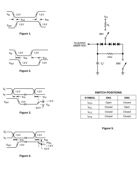
AC WAVEFORMS
1.3 V
1.3 V
1.3 V
1.3 V
1.3 V
1.3 V
1.3 V
V
INV
OUTt
PLHt
PHL1.3 V
1.3 V
V
INV
OUTC
L*
SW2
5 k
Ω
SW1
V
CCR
LTO OUTPUT
UNDER TEST
1.3 V
t
PHLt
PLHV
EV
EV
OUTV
EV
EV
OUTt
PHZ1.3 V
1.3 V
t
PZLt
PLZV
OL1.3 V
≥
V
OH0.5 V
t
PZH1.3 V
Figure 1.
Figure 2.
Figure 3.
[image:4.612.104.548.80.705.2]Figure 4.
Figure 5.
≈
1.3 V
0.5 V
≈
1.3 V
SWITCH POSITIONS
Closed
Open
Closed
Closed
Open
Closed
Closed
Closed
t
PZHt
PZLt
PLZt
PHZSW2
SW1
PACKAGE DIMENSIONS
N SUFFIX
PLASTIC PACKAGE
CASE 738–03
ISSUE E
NOTES:
1. DIMENSIONING AND TOLERANCING PER ANSI Y14.5M, 1982.
2. CONTROLLING DIMENSION: INCH. 3. DIMENSION L TO CENTER OF LEAD WHEN
FORMED PARALLEL.
4. DIMENSION B DOES NOT INCLUDE MOLD FLASH.
M
L
J
20 PLM
B
M
0.25 (0.010)
T
DIM MININCHESMAX MILLIMETERSMIN MAX
A 1.010 1.070 25.66 27.17
B 0.240 0.260 6.10 6.60
C 0.150 0.180 3.81 4.57
D 0.015 0.022 0.39 0.55
G 0.100 BSC 2.54 BSC
J 0.008 0.015 0.21 0.38
K 0.110 0.140 2.80 3.55
L 0.300 BSC 7.62 BSC
M 0 15 0 15
N 0.020
0.040 0.51 1.01E
1.27 1.77 0.050 0.070
1
11
10 20
–A–
SEATING PLANE
K
N
F
G
D
20 PL–T–
M
A
M
0.25 (0.010)
T
E
B
C
D SUFFIX
PLASTIC SOIC PACKAGE
CASE 751D–05
ISSUE F
20
1
11
10
B
20XH
10X
C
L
18X
A1
A
SEATING PLANE
h
X 45
E
D
M
0.25
M
B
M
0.25
T
A
SB
Se
T
B
A
DIM MILLIMETERSMIN MAX
A 2.35 2.65
A1 0.10 0.25
B 0.35 0.49
C 0.23 0.32
D 12.65 12.95
E 7.40 7.60
e 1.27 BSC
H 10.05 10.55
h 0.25 0.75
L 0.50 0.90
0 7
NOTES:
1. DIMENSIONS ARE IN MILLIMETERS. 2. INTERPRET DIMENSIONS AND TOLERANCES
PER ASME Y14.5M, 1994.
3. DIMENSIONS D AND E DO NOT INCLUDE MOLD PROTRUSION.
4. MAXIMUM MOLD PROTRUSION 0.15 PER SIDE. 5. DIMENSION B DOES NOT INCLUDE DAMBAR
PROTRUSION. ALLOWABLE PROTRUSION SHALL BE 0.13 TOTAL IN EXCESS OF B DIMENSION AT MAXIMUM MATERIAL CONDITION.
ON Semiconductor and are trademarks of Semiconductor Components Industries, LLC (SCILLC). SCILLC reserves the right to make changes without further notice to any products herein. SCILLC makes no warranty, representation or guarantee regarding the suitability of its products for any particular purpose, nor does SCILLC assume any liability arising out of the application or use of any product or circuit, and specifically disclaims any and all liability, including without limitation special, consequential or incidental damages. “Typical” parameters which may be provided in SCILLC data sheets and/or specifications can and do vary in different applications and actual performance may vary over time. All operating parameters, including “Typicals” must be validated for each customer application by customer’s technical experts. SCILLC does not convey any license under its patent rights nor the rights of others. SCILLC products are not designed, intended, or authorized for use as components in systems intended for surgical implant into the body, or other applications intended to support or sustain life, or for any other application in which the failure of the SCILLC product could create a situation where personal injury or death may occur. Should Buyer purchase or use SCILLC products for any such unintended or unauthorized application, Buyer shall indemnify and hold SCILLC and its officers, employees, subsidiaries, affiliates, and distributors harmless against all claims, costs, damages, and expenses, and reasonable attorney fees arising out of, directly or indirectly, any claim of personal injury or death associated with such unintended or unauthorized use, even if such claim alleges that SCILLC was negligent regarding the design or manufacture of the part. SCILLC is an Equal Opportunity/Affirmative Action Employer.
PUBLICATION ORDERING INFORMATION
CENTRAL/SOUTH AMERICA:
Spanish Phone: 303–308–7143 (Mon–Fri 8:00am to 5:00pm MST) Email: ONlit–[email protected]
NORTH AMERICA Literature Fulfillment: Literature Distribution Center for ON Semiconductor P.O. Box 5163, Denver, Colorado 80217 USA
![Clinical evaluation of [123I]FP-CIT SPECT scans on the novel brain-dedicated InSPira HD SPECT system: a head-to-head comparison](data:image/gif;base64,R0lGODlhAQABAIAAAP///wAAACH5BAEAAAAALAAAAAABAAEAAAICRAEAOw==)