Implementation of FPGA based PID Controller for DC
Motor Speed Control System
Savita Sonoli K.Nagabhushan Raju
Abstract— In this paper, the implementation of software module using ‘VHDL’ for Xilinx FPGA (XC3S400) based PID controller for DC motor speed control system is presented. The tools used for building and testing the software modules are Xilinx ISE 9.2i and ModelSim XE III 6.3c. Before verifying the design on FPGA the complete design is simulated using Modelsim Simulation tool. A test bench is written where, the set speed can be changed for the motor. It is observed that the motor speed gradually changes to the set speed and locks to the set speed.
IndexTerms— Field Programmable Gate Array (FPGA), Proportional-Integral-Derivative (PID) controller, Very High Speed Integrated Circuit Hardware Description Language (VHDL), Pulse Width Modulation (PWM).
I. INTRODUCTION
Hardware Description Languages (HDLs) are used to describe hardware for the purpose of Simulation, Modeling, Testing, Design, and Documentation of digital systems. The most popular HDLs are VHDL [(Very High Speed Integrated Circuit) Hardware Description Language], and Verilog. VHDL is used to describe hardware from the abstract to the concrete level. Many of the Electronic Design Automation (EDA) vendors are standardizing on VHDL as input and output from their tools. These tools include simulation tools, synthesis tools, layout tools and testing tools.
The Proportional-Integral-Derivative (PID) controllers have been widely used over the past five decades due to their simplicity, robustness, effectiveness and applicability for a broad class of systems. Despite the numerous control design approaches that have appeared in the literature, it is estimated that, nowadays PID controllers are still employed in more than 95% of industrial processes [1]. For many decades, the digital PID controller has been used extensively in real time digital control. The PID is used extensively in the field of servo motor control, robotics, temperature control and power electronics. It has a long history of development and very mature tuning rules. Overall, the PID is an important tool for the embedded real time digital control designer. They are usually implemented either in hardware using analog components or in software using computer-based systems. The emergence of field programmable gate arrays and hardware description languages allows for added dimensions of digital PID controllers, Parallelism, Programmable bit widths and absolute determinism.
Dr. Savita Sonoli is Professor and Head Department of Instrumentation Technology, Proudha Devaraya Institute of Technology, HOSPET-583225,KARNATAKA.INDIA. (e-mail: [email protected])
Dr. K.Nagabhushan Raju is Associate Professor and Head Department of Instrumentation. Sri Krishnadevaraya University,Ananthpur-515055,AndraPradesh, INDIA. (e-mail: [email protected])
Building PID controllers on Field Programmable Gate Arrays (FPGAs) improves speed, accuracy, power-efficiency, compactness and cost effectiveness.
With the growing complexity of motor and motion control applications, it becomes apparent that a Field Programmable Gate Array (FPGA) offers significant advantage over the off shelf Application Specific Standard Product (ASSP) solutions in the areas of performance, flexibility and inventory control [2]. Custom motor drive interfaces such as Pulse Width Modulation (PWM) can be developed easily, quickly and at low cost. Additionally, because of full configurability, the same FPGA can be used in various product ranges, reducing the need to maintain inventory for multiple devices [3].
The Spartan3 family of Field-Programmable Gate Arrays is specifically designed to meet the needs of high volume, cost-sensitive consumer electronic applications. The eight-member family offers densities ranging from 50,000 to five million system gates. Because of their exceptionally low cost, Spartan3 FPGAs are ideally suited to a wide range of consumer electronic applications, including broadband access, home networking, display/projection and digital television equipment. Modern FPGAs and their distinguishable capabilities have been advertised extensively by FPGA vendors [4]. Moreover, some refereed articles addressed the advantages of utilizing these powerful chips [5][6]. In the past two years, Spartan II and III FPGA families from Xilinx have been successfully utilized in a variety of applications, which include inverters [7][8], communications [9][10], embedded processors [11], and image processing [12]. The implementation of PID controllers using microprocessors and Digital Signal Processor (DSP) chips is old and well known [13][14], whereas very little work can be found in the literature on how to implement PID controllers using FPGAs. A PWM generator is introduced in [15]. However, only simulation results are presented. The contributions of the authors in [16][17] are considered complementary to the present work as they provide tools for building the current application. The software developed provides the user interface through on board peripherals like Pushbuttons, Toggle switches, Light Emitting Diodes (LEDs) and Seven Segment Displays, so that the user can change the set speed of the motor as well view the data display on Seven Segment Display and also reset the entire system.
II. OVERVIEW OF FUNCTIONAL MODULES
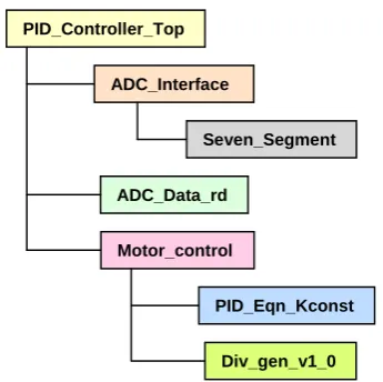
The target FPGA device used in the present work is Spartan3 family XC3S400 manufactured by Xilinx. Design development and debugging is carried on a low-cost, full-featured kit from Advanced Electronic Systems (ALS). This board provides all the tools required to design and verify Spartan3 platform designs. Designs are based on 10 MHz clock. Figure 1 shows the Hierarchical Diagram of FPGA Based PID Controller Implementation for DC motor speed control system. Figure 2 shows the PID Controller Top level module with sub modules with internal and external signal flow. The software tools used for building and testing these modules are Xilinx ISE 9.2i and ModelSim XE III 6.3c.
A. PID controller Top module
The PID Controller Top module is the Main Top level VHDL module in the hierarchy. It instantiates the sub modules ADC_interface, ADC_Data_Read and Motor_control modules. It interconnects all the signals and interacts with the external world.
B. ADC interface module
It is a front end interface module for ADC. This module has a state machine ADC_state that gives out the signals Start Of Conversion (SOC) and Output Enable (OE) for ADC. It also generates ADC channel address based on the three bit
Fig. 1. Hierarchical Diagram for FPGA based PID controller Implementation
on board toggle switch (TS1, TS2, TS3) input. After asserting these signals it waits for End Of Conversion (EOC) signal, which is 8th bit in the data bus. Once ADC asserts EOC the state machine generates the ADC_Data_Ready signal used as enable for the register that latches the valid data from the ADC. Also the same signal will be given to the next module, ADC Data Read module that uses this as a control signal for latching the valid data The Sub module Seven_Segment is used for seven segment Display that will display the data going to Digital to Analog Converter (DAC) hardware module, which is the actual speed, calculated using the PID equation.
ADC_Interface
Seven_Segment
ADC_Data_rd
Motor_control
PID_Eqn_Kconst
Div_gen_v1_0
ADC_Interface
ADC_Data_rd
Motor_control Seven_Segment
PID_Eqn_Kconst Div_gen_v1_0
Reset in
LED_out
Seven_seg_out SOC_out
OE_out
OE4_Disp
OE2_Disp OE1_Disp
OE3_Disp
Clk_Div8_out
Clk_10MHz_in ADC_Data_in
DAC_data_out
DAC_data_out ADC_Data
ADC_Data_rdy
ADC_Address_in ADC_Addr_out
ADC_Data_rdy ADC_Data
Speed_select_in
Capture_ctrl_in
[image:2.595.350.523.69.241.2]K_Equation en, en-1, en-2 Error Data
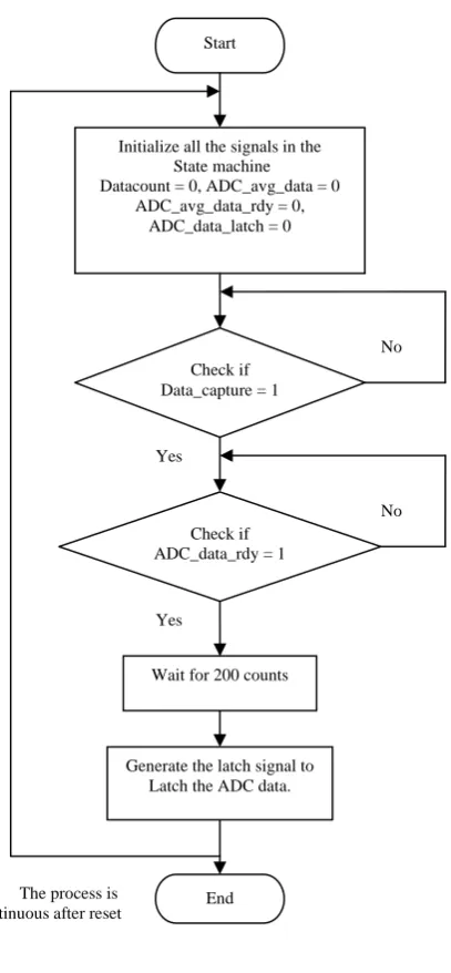
C. ADC data read module
The ADC data read module takes the ADC data from ADC interface module based on the control signal ADC_data_rdy_in. It has a state machine ADC_RD_State which checks for ADC_data_capture switch, a toggle switch input connected to the switch input capture_ctrl_in (TS16) in top module. Once this switch is asserted it proceeds to next state and checks for the ADC_Data_ready input signal from ADC interface module. When the ADC_Data_ready signal is asserted it will wait for 200 cycles in next state and asserts ADC_AVG_DATA_Rdy signal, which will register the 200th ADC data. Process waits 200 cycles for ADC data to get stabilized after change in speed of motor. The latched data along with the control signal ADC_AVG_DATA_Rdy will be sent out to next module, which is Motor control module.
D. Motor control module
The Motor control module receives the data from ADC Data Read module, which is latched into the module using ADC_AVG_DATA_Rdy control signal from the ADC Data read module. Once the data is latched into the module it calculates the current speed, which is the ADC data multiplied by 10. The maximum speed for the motor is considered as 2550 rpm which if divided by 10 to get 255 in decimal, equivalent to “11111111” in binary, which is the maximum 8 bit ADC value. This is done to get the approximated current speed.
Once the current speed is calculated, this value is subtracted with the set speed value, which is set using the toggle switches Speed_Set_switch, connected to Speed_select_in, in PID controller top module. This will generate current error en. The same en will become en-1 and 2 in next consecutive cycles. The values of en, 1 and en-2 are fed to PID equation calculation module with their polarity, which indicates whether the calculated value is positive or negative. The PID Equation calculation module will calculate K_equation value, which is a part of PID equation, [Kp *( en - en-1) + Ki * en + Kd *( en - 2*( en-1))+ en-2 ]. The final PID equation
[Vn-1+ Kp *( en - en-1) + Ki * en + Kd *( en - 2*( en-1))+ en-2] will be calculated in Motor control module. It has several state machines like Motor_Control_State, PID_Assign_State, SW_Debounce_State and Speed_Lock_State.
In Motor_Control_State machine capture enable switch is monitored which is connected to Captur_ctrl_in switch in the top module. Once this is asserted the controller waits for some delay until valid data for PID equation is calculated. Now, swap the values of errors en, en-1 and en-2 and also PID values Vn and Vn-1 are swapped.
PID_Assign_State machine checks the calculated PID value for negative or greater than 255 the maximum value of ADC. If it is negative then DAC is assigned Zero, else if the value is greater than 255, 255 is assigned. If the value is between 0 and 255 then the actual value for DAC is assigned.
SW_Debounce_State machine wait for some fixed amount of delay to overcome the de-bouncing of the speed select toggle switches.
Speed_Lock_State machine check whether the calculated speed lies with in plus or minus 100 rpm range of set speed, if so, it is approximated to the set speed. This approximation is done, as floating point operation is not considered in calculating the PID equation, which is beyond the scope of this design. Once the calculated speed is ready by PID equation, it is divided by 10 using the divider module to get the equivalent DAC value. This is based on the approximation for rpm, which was done in the beginning while calculating the current speed from ADC data. Once the equivalent binary data is calculated from PID equation it is sent to DAC. This will continue until all the errors become zero and Vn equals Vn-1, which forces current speed equal to set speed and hence motor starts running at set speed. E. Coregen divider module
This is Xilinx specific coregen module, used in the present design. Instantiated in Motor Control Module to divide the calculated PID value Vn to get the equivalent binary value, which has to be sent to DAC.
F. Seven segment display module
This module will generate the output enable for on board seven segment displays and also provide the data to seven segment modules, which is going out to DAC.
G. PID equation calculation module
The calculated errors en, en-1 and en-2 with their polarities, whether they are positive or negative is fed to this module from motor control module. This module will calculate the part of PID equation,
Vn = Vn-1+ Kp *( en - en-1) + Ki * en + Kd *( en - 2*( en-1))+ en-2 which is Kp *( en - en-1) + Ki * en + Kd *( en - 2*( en-1))+ en-2. The constants Kp, Ki and Kd values are 3, 2 and 1 respectively. They are calculated by trial and error method. The PID equation is evaluated part by part. First the values for Kd *( en - 2*( en-1)) , Ki * en and Kp *( en - en-1) are individually calculated retaining their polarity, which will determine whether the calculated values are positive or negative. Once this is done combined equations,
Kd *( en - 2*( en-1))+ en-2 and Kp *( en - en-1) + Ki * en are calculated with their polarities. Once these equations are evaluated, the final K_equation is calculated which is, Kp *( en - en-1) + Ki * en + Kd *( en - 2*( en-1))+ en-2. This is fed back to Motor control module with K_equation polarity that will determine, whether the calculated value of K equation is positive or negative. In motor control module the final PID equation,
Vn = Vn-1+ Kp *( en - en-1) + Ki * en + Kd *( en - 2*( en-1))+ en-2 is calculated. Here the polarities of current errors and current PID value are passed to polarities of previous PID and previous errors to hold their polarity for further calculations. For example, if the error en and its polarity calculated are negative, then in the next cycle the en value is assigned to en-1 and the polarity of en becomes en-1 polarity.
III. STATE FLOW DIAGRAMS
ADC_State, state machine in ADC Interface module. Figure 4 shows State flow diagram for ADC_RD_State, state machine in ADC Data read module similarly, State flow diagrams for Motor_Control _State, state machine, PID_Assign_State, state machine, SW_Debounce State, state machine, and Speed_lock_state, state machine in Motor control module are developed.
Fig. 3. State flow diagram for ADC_State, state machine
IV. RESULTS
A. Simulation Results
Logic simulation in FPGA design environment plays a very vital role in verifying the functionality of the designs. Simulation is a powerful way to test the system on a computer, before it is turned into hardware. Simulators let designer to check the values of signals inside the system.
[image:4.595.62.280.173.614.2]In the present study, for functional verification, before verifying the performance of proposed controller design on FPGA,
Fig. 4. State flow diagram for ADC_RD_State, state machine
the complete design is simulated using Modelsim Simulation tool (Xilinx version ModelSim XE III 6.3c), which has pre-compiled libraries for all Xilinx FPGAs. A test bench is written where, the set speed can be changed for the motor. In the test bench, the Top module of the design PID_controller_top is instantiated. The inputs like Clock, Reset, Switch data and ADC data are defined and the output is observed in the simulation window.
As many sub modules are instantiated in Top module and as this is a hierarchical design, internal sub module signals are also observed in the waveform window of the simulator. Once all the signals are taken into the waveform window, the simulation is run for 1000 µs and the changes in the signals are observed in the waveform window. It is observed that the motor speed gradually changes to the set speed and locks to the set speed.
Start
Initialize all the signals ADC_SOC = 0, ADC_Data_ready = 0
ADC_OE = 0
Assert ADC_data ready = 1 &
ADC_ OE = 1
End The process is
continuous after reset
Check If EOC = 1 Assert SOC = 1
& OE = 1
Yes
No
Start
Initialize all the signals in the State machine Datacount = 0, ADC_avg_data = 0
ADC_avg_data_rdy = 0, ADC_data_latch = 0
Check if Data_capture = 1
Check if ADC_data_rdy = 1
Wait for 200 counts
Generate the latch signal to Latch the ADC data.
End The process is
continuous after reset
No
No
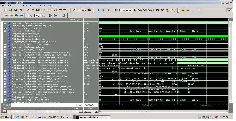
Figure 5 shows the simulation results for the set speed of 1400 rpm. It is seen that after certain transitions, when the errors en, en-1 and en-2 become zero, the current speed will become 1400 rpm which is equal to set speed. The data going to the DAC, PID_data_out is equal to 140, which is the current speed. The transitions in the state machines that are assigning current value to en, en-1, en-2 and Vn-1 are observed in the waveform window.
Finally, from the waveforms it is observed that, when the optimal values for Kp, Ki and Kd are used to calculate the
current speed, the current speed will equal the set speed when all the errors en, en-1 and en-2 become zero, hence Vn equals Vn-1 and the motor starts running at the set speed.
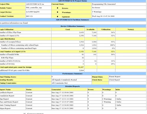
Table 2 shows the Design Summary, Xilinx tool device utilization summary and reports the percentage of available resources that have been used for the current FPGA design. The performance summary summarizes the timing requirement and also the proper routing of the signals.
[image:5.595.100.481.217.413.2]
Fig. 5. Simulation waveforms for set speed 1400 rpm
B. Hardware Test Results
The experimental studies are carried out to evaluate the performance of the controller. Configuration is the Process by which the bit streams of a design, as generated by the development software are loaded into the internal configuration memory of the FPGA. To verify the performance of the controller design on Hardware, the VHDL code (Bit file) is downloaded into the Target FPGA device (Spartan3 family XC3S400) and the complete system is reset. The set speed is assigned to switches according to the requirement and the capture control switch is enabled. Once this is done the ADC data will be read and PID equation implemented will calculate the equivalent PID value and it is fed back to the motor through DAC and once the current speed equals the set speed, the motor starts running at the set speed. Again to change the set speed, the above procedure is repeated by changing the toggle switch position.
As the set speed is varied, the ADC voltage also varies, the measured ADC values and the equivalent Hex values for different set speeds are tabulated. It is observed that the current speed, which is displayed, on the ‘on board’ seven segment display equals the set speed value. Also the change in the motor speed for different switch combinations can be observed accordingly. Table 1 shows the results of the DC motor speed control system for various set speeds.
Figure 6 shows the Photograph of the experimental setup and working model of FPGA based DC motor speed control system.
Table1. Results of DC motor speed control system for various set speeds
Sl.No
Toggle Switch position
Set Speed (rpm)
Equivalent HEX value
Measured ADC voltage
(Volts)
1. 000 2500 FA 4.5
2. 001 1200 78 2.4
3. 010 400 28 0.64
4. 011 1400 8C 2.8
5. 100 2000 C8 3.63
6. 101 600 3C 1.15
7. 110 1100 6E 2.04
8. 111 900 5A 1.8
Table 2. Design Summary of FPGA based PID controller for DC motor Speed control system ADCINTERFACE Project Status
Project File: ADCINTERFACE.ise Current State: Programming File Generated
Module Name: PID_controller_top Errors: No Errors
Target Device: xc3s400-5pq208 Warnings: 3 Warnings
Product Version: ISE 9.2i Updated: Wed Aug 20 13:47:36 2008
ADCINTERFACE Partition Summary No partition information was found.
Device Utilization Summary
Logic Utilization Used Available Utilization Note(s)
Number of Slice Flip Flops 2,638 7,168 36%
Number of 4 input LUTs 2,358 7,168 32%
Logic Distribution
Number of occupied Slices 1,916 3,584 53%
Number of Slices containing only related logic 1,916 1,916 100%
Number of Slices containing unrelated logic 0 1,916 0%
Total Number of 4 input LUTs 2,358 7,168 32%
Number of bonded IOBs 43 141 30%
IOB Flip Flops 16
Number of MULT18X18s 3 16 18%
Number of GCLKs 2 8 25%
Total equivalent gate count for design 56,447
Additional JTAG gate count for IOBs 2,064
Performance Summary
Final Timing Score: 0 Pinout Data: Pinout Report
Routing Results: All Signals Completely Routed Clock Data: Clock Report
Timing Constraints: All Constraints Met
Detailed Reports
Report Name Status Generated Errors Warnings Infos
Synthesis Report Current Sun Aug 17 12:30:06 2008 0 0 0
Translation Report Current Sun Aug 17 12:30:48 2008 0 0 0
Map Report Current Sun Aug 17 12:31:18 2008 0 2 Warnings 3 Infos
Place and Route Report Current Sun Aug 17 12:33:47 2008 0 1 Warning 3 Infos
Static Timing Report Current Sun Aug 17 12:34:08 2008 0 0 3 Infos
Bitgen Report Current Sun Aug 17 12:34:53 2008 0 0 0
V. CONCLUSIONS
A digital PID controller is successfully implemented using the FPGA and its performance is verified and tested on a DC motor speed control system for real-time control. The test results showed that with PID controller added, the steady-state error is eliminated and the desired output speed is obtained. The implementation of controller has reduced the total hardware complexity and cost. According to the experiment done it is observed that, in the simulation, when the set speed is changed, the motor speed locks to the set speed, when the current error en, previous error en-1 and previous to the previous error en-2 becomes zero.
In brief, the role of FPGA, in measurement and control point of view, is to acquire the data from sensor through analog to digital converter, do the processing on the acquired data and then generate control signals to the actuator, which intern controls the parameter being measured. FPGAs ensure ease of design, lower development costs, more product revenue, and the opportunity to speed products to market. Building PID controllers on FPGAs improves speed, accuracy, power-efficient, compactness and cost effectiveness over other digital implementation techniques.
REFERENCES
[1] K.J. Astrom and T. H. Hagglund, “New Tuning Methods far PID Controllers,” Proc. of 3rd European Conference, pp. 2456-2462, 1995. [2] Shouling He and Xuping Xu, “Hardware/Software Co design
Approach for an ADALINE Based Adaptive Control System,” Journal of Computers, vol. 3, no. 2, pp. 29-36, Academy publisher, February 2008.
[3] Craig Hackney, “PGA Motor Control Reference Design,” Application Note: Spartan and Virtex FPGA Families, Xilinx XAPP808 vol. 1.0, September 16, 2005.
[4] Mohamed Abdelati, “FPGA-Based PID Controller Implementation,” The Islamic University of Gaza, Palestine, This research was supported by the Ministry of Higher Education in Palestine.
[5] Anthony Cataldo, “Low-priced FPGA options set to expand,” Electronic Engineering Times Journal, no. 1361, pp. 38-45, USA, 2005.
[6] Gordon Hands, “Optimised FPGAs vs dedicated DSPs,” Electronic Product Design Journal, vol. 25, no. 12, UK, December 2004. [7] R. Jastrzebski, A. Napieralski, O. Pyrhonen and H. Saren,
“Implementation and simulation of fast inverter control algorithms with the use of FPGA circuit,” Nanotechnology Conference and Trade Show, pp. 238-241, Nanotech 2003.
[9] Bouzid Aliane and Aladin Sabanovic, “Design and implementation of digital bandpass FIR filter in FPGA,” Computers in Education Journal, vol.14, pp. 76-81, 2004.
[10] M. Canet, F. Vicedo, V. Almenar and J. Valls, “FPGA implementation of an IF transceiver for OFDM-based WLAN,” IEEE Workshop on Signal Processing Systems, SiPS: Design and Implementation, pp. 227-232, USA, 2004.
[11] Xizhi Li and Tiecai Li, “ECOMIPS: An economic MIPS CPU design on FPGA,” Proceedings- 4th IEEE International Workshop on System-on-Chip for Real-Time Applications, pp. 291-294, Canada 2004.
[12] R. Gao, D. Xu and J. P. Bentley, “Reconfigurable hardware implementation of an improved parallel architecture for MPEG-4 motion estimation in mobile applications,” IEEE Transactions on Consumer Electronics, vol.49, no.4, November 2003.
[13] H. D. Maheshappa, R. D. Samuel and A. Prakashan, “Digital PID controller for speed control of DC motors, IEEE Technical Review Journal, vol. 6, no.3, pp. 171-176, India, 1989.
[14] J. Tang, “PID controller using the TMS320C31 DSK with on-line parameter adjustment for real-time DC motor speed and position control,” IEEE International Symposium on Industrial Electronics, vol. 2, pp. 786-791, Pusan, 2001.
[15] D. Deng, S. Chen and G. Joos, “FPGA implementation of PWM pattern generators,” Canadian Conference on Electrical and Computer Engineering, and Electronics Engineers Inc, vol. 1, pp. 225-230 May, 2001.
[16] Rivera. D.E, S. Skogestad and M. Morari, “Internal Model Control 4. PID Controller Design.” Ind. Ene Chem. Proc. Des & Dev, 25, pp. 252.265, 1986.