Introducing Semi-programmable Hardware to a
Real High-Level Synthesis Tool
Akira Yamawaki
∗Seiichi Serikawa
†Masahiko Iwane
‡Abstract– The semi-programmable hardware is a design-level hardware architecture residing on the pass where C program with memory access is con-verted to hardware. The SPHW realizes the mem-ory access controller and buffer by writing the soft-ware program and parameters respectively. Com-pared with the cases that use only HDL, the SPHW which can design the efficient memory controllers at C-level abstraction reduces the development time sig-nificantly. In addition, the SPHW shows the compa-rable performance compared to the HDL hardware containing the custom memory controller even if it is written at high-abstraction in the SPHW. In gen-eral, the high-level synthesis tool whose design entry is C program is often used to reduce the burden de-signing the data processing hardware. However, the SPHW has not been introduced into any HLS tech-nology yet. This paper develops the true C level-design environment including the SPHW as the data processing hardware on a real commercial HLS tool, Handel-C. By using the SPHW providing the register-based data interface to the data processing hardware, we demonstrate that the HLS tool can easily write the hardware accessing to the memory in C language. This is because this interface hides the detail of the memory devices and the memory access patterns, by providing the data processing hardware with the sim-ple stream data. For hiding memory access latency, the simple software-pipelining can be applyed to the memory access program and parameters of the buffer. Consequently, the designer can realize the data pro-cessing hardware with data-prefetching mechanism at the complete C-level design entry.
Keywords: high-level synthesis, hardware design, mem-ory latency hiding, system-on-chip, hardware architec-ture
1
Introduction
For the design of the system-on-chips, the high-level syn-thesis (HLS) technologies generating the hardware from
∗This research was partially supported by the Kayamori Foun-dation of Informational Science Advancement and the Grant-in-Aid for Young Scientists (B) (22700055). Faculty of Engineering, Kyushu Institute of Technology, 1-1, Sensui, Tobata, Kitakyushu, Fukuoka 804-8550 Japan. Email: [email protected]
†Faculty of Engineering, Kyushu Institute of Technology, 1-1, Sensui, Tobata, Kitakyushu, Fukuoka 804-8550 Japan.
‡Adviser of Yuundo Co.,Ltd. Japan.
C program have been researched and developed [1–7]. The HLS tool can reduce the design burden significantly due to the high design abstraction. Generally, the HLS technologies are good at generating an efficient data pro-cessing hardware assuming simple and typical data access patterns like the stream data. For example, some com-pilers of the HLS support only the dedicated memory access pattern [4, 6, 7]. Across the users, the application programs and the buffering methods, the memory access patterns are different. Thus, the memory accesses are hard to be treated systematically by an algorithmic way. In addition, the memory access latency cannot be hidden by the data prefetching [8] implicitly [1–7]. To hide the memory latency, the hardware has to be written skill-fully in the C description with the deep knowledge of the used HLS tool and target device. As a result, the HLS tool might generate the hardware including an efficient memory access controller. Even if the HLS tool is used, such burden may be comparable to designing a custom memory access controller from scratch in a hardware de-scription language (HDL).
To tackle the problems mentioned above, we have proposed a design-level hardware architecture (semi-programmable hardware: SPHW) which is inserted onto the pass converting the C program to the hardware [9]. The SPHW realizes the memory access controller and the buffer by writing the software program and param-eters respectively. Compared with the design cases that use the HDL, the SPHW which can design the efficient memory controllers at C-level abstraction reduces the de-velopment time significantly [9]. In addition, the SPHW shows the comparable performance compared to the HDL hardware containing the custom memory controller even if it is written at high-level abstraction [9].
SPHW Optional
يSYNC0ً GPR
MB
FSM EXU
RRF
SPHW Optional
LSU
DBRI
Data Path
يSYNC0ً
يEXE0ً RRF
DBRO Memory
SM LSU
MEM WR يSYNCjً
يEXEiً DBRO
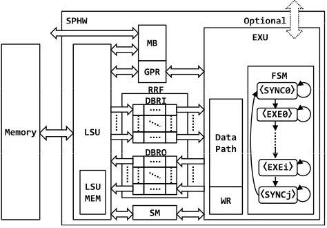
Figure 1: Block Diagram of SPHW
software-pipelining with double buffering to hide mem-ory access latency is easily implemented into the data processing hardware at high-level abstraction.
The rest of the paper is organized as follows. Section 2 describes the overview of the SPHW. Section 3 shows the design flow using the SPHW. Section 4 demonstrates the SPHW mapping by using an example of the color con-version from RGB to YCrCb. Section 5 performs some preliminary experiments and shows the experimental re-sults. Finally, Section 6 concludes the paper.
2
SPHW Architecture
2.1
Organization
Fig. 1 shows the organization of the SPHW. The load/store unit (LSU) transfers the data between mem-ory and reconfigurable register file (RRF). The programs to be executed by the LSU are stored in the LSU memory (LSUMEM). The execution unit (EXU) is data process-ing hardware. The synchronization mechanism (SM) per-forms the producer-consumer synchronization between the LSU and the EXU. The producer performs the re-lease synchronization to invoke the consumer waiting for the data on the RRF by the wait synchronization.
The reconfigurable register file (RRF) consists of the input/output data buffer registers (DBRI and DBRO). They have one or more banks which contain one or more entries. The number of the banks and entries are con-figurable by the parameters. Thus, the suitable buffer for the data processing hardware on the EXU can be implemented by parameters. The mailbox (MB) is con-trol/status registers for the SPHW. The external modules can check the statuses of the SPHW via mailboxes. The parameters required for the SPHW execution can be set via the mailboxes. The general purpose register (GPR) is used by the LSU and the EXU.
The EXU has the finite state machine (FSM), the working
Loadline
LLS(B/Be/BE/E/Eb/EB,mem addr,str width,numoftrans,sync) LLS(B/Be/BE/E/Eb/EB,mem addr,str width,numoftrans,sync)
Loadword
LWS(B/BE/E/EB,mem addr,str width,numoftrans,sync)
Storeline
SLS(B/Be/BE/E/Eb/EB,mem addr,str width,numoftrans,sync)
Storeword
SWS(B/BE/E/EB dd t idth ft ) SWS(B/BE/E/EB,mem addr,str width,numoftrans,sync)
B:Incrementthebankpointerpereachwordtransfer. Be:Incrementthebankpointerpereachwordtransfer. Incrementtheentrypointerpereachlinetransfer. BE:Incrementthebankpointerpereachwordtransfer.
Incrementtheentrypointerwhenalloftransfersfinish. E:Incrementtheentrypointerpereachwordtransfer. Eb:Incrementtheentrypointerpereachwordtransfer. Incrementtheentrypointerpereachlinetransfer. EB:Incrementthebank pointerpereachwordtransfer.
[image:2.595.52.289.73.238.2]Incrementtheentrypointerwhenalloftransfersfinish Incrementtheentrypointerwhenalloftransfersfinish.
Figure 2: Load/Store instructions of LSU
registers (WR) and the data path. The FSM has the states (⟨EXEi⟩) to control the data path. In addition, the states (⟨SYNCi⟩) to synchronize the LSU are inserted.
2.2
Memory Access
The LSU has the load/store instructions per the word and the line containing continuous words as shown in Fig. 2. Each of instructions can specify the number of transfers and the stride width per each word/line transfer. That is, the LSU can perform the gather/scatter operations by one instruction. Since the load/store instructions have the synchronization field, the synchronization can be also performed simultaneously with the memory access. The pointers to the bank and entry can be incremented au-tomatically according to the notation in the instruction. The LSU converts the distributed data in the memory to the streamed data in the RRF, executing the sophis-ticated load/store instructions.
Fig. 3 (a) shows the examples implementing a double buffer for the streaming data. We assume that the line contains 4 words, the number of banks of the DBRI is 8 and each bank contains 2 entries. Fig. 3 (b) shows an example loading the 4×4 window. In this example, the DBRI has 4 banks containing 4 entries. As shown in these examples, the LSU can easily realize the sophisticated memory accesses.
3
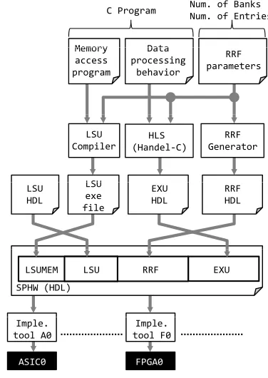
SPHW Design Flow
Fig. 4 shows the framework of the design flow which employs the SPHW. In this case, we employ the Handel-C [1] as the HLS tool for the EXU.
LLS(BE,img,4*sizeof(pixel),2,RLS);
1 2 3 4 5 6 7 8
pixelplain_text[num]
DBRI 1 2 bank0
b k
9 10 2 3 4 bank1 bank2
bank3 EXU
5 6 bank4 bank5
10 11 12 13 14
e
n
t
r
y
0
e
n
t
r
y
1
7 8 bank6 bank7
15 16
LLS(Be,img,width*sizeof(pixel),4,RLS);
1 2 3 4
pixelimg[height][width]
DBRI
(a)Doublebufferingforstreamdata
1 2 3 4
5 6 7 8 1 5 9 13
2 6 10 14 3 7 11 15 4 8 12 16 bank0
bank1 bank2 bank3
0 1 2 3
9 10 11 12 13 14 15 16
h
e
i
g
h
t EXU
e
n
t
r
y
0
e
n
t
r
y
1
e
n
t
r
y
2
e
n
t
r
y
3
width
[image:3.595.57.288.69.344.2](b) 4x4WindowLoading
Figure 3: Example of Load Instruction
sophisticated access patterns are put into the RRF as the stream data by the LSU.
The Handel-C is based on the concept of the commu-nicating sequential processes (CSP) model [10] whose input/output are the streaming interface. Thus, the Handel-C hardware is a good candidate as the EXU to be connected to the RRF1.
Since the LSU and the EXU are executing individually across the RRF, the memory access by the LSU can over-lap onto the data process by the EXU. By using the SPHW, the designer can design the hardware with the data prefetching mechanism [8] easily in the high-level description using the program and parameters.
4
Mapping Example
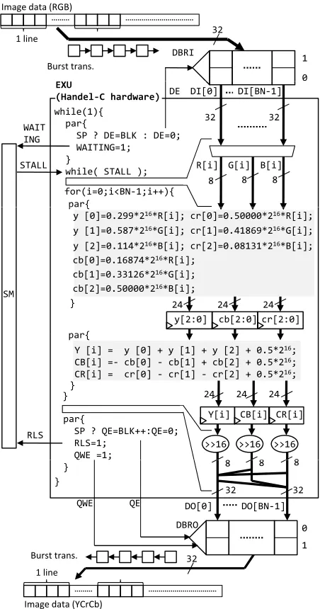
Fig. 5 and Fig. 6 show an example of mapping the color conversion from RGB to YCrCb into the SPHW. The former writes the hardware behavior in Handel-C. The latter writes the LSU program in C-like language. We have developed the tool converting the LSU program to the machine code by perl.
Now, we assume that the pixel of the image data is 32bit containing each of 8bit-R, G and B data. In this version, the SPHW supports the following features.
1Most HLS tool is good at converting the stream processing to
the hardware [1–7].
C Program Num.ofBanks Num.ofEntries
Memory Data Memory
access program
Data processing
behavior
RRF parameters
LSU Compiler
HLS (HandelŞC)
RRF Generator
LSU LSU exe file
EXU HDL
RRF HDL LSU
HDL
SPHW(HDL)
LSU RRF EXU
LSUMEM
Imple. toolA0
ASIC0
Imple. toolF0
[image:3.595.330.518.73.338.2]FPGA0
Figure 4: SPHW Design Flow When Using Handel-C
(1) The number of words in the line is 4. The word width is 32bit.
(2) The width of each bank of the DBRI/O is 32bit.
(3) The LSU supports the burst transfer containing 4 words.
(4) The LSU is the pipelined scalar processor with 3 stages.
Fig. 5 shows an overview of mapping to the SPHW. The RGB data in the memory is loaded by the LSU into the DBRI. The EXU waits until the RGB data needed is stored into the DBRI. When the LSU loads the RGB data and releases the EXU, the EXU starts to process the RGB data in the DBRI and stores YCrCb data into the DBRO. Then the EXU releases the LSU waiting the YCrCb data. After this, the LSU stores the YCrCb data into the memory.
DBRI
0 1
Imagedata(RGB)
1line
Bursttrans.
32
R[i] G[i] B[i]
DI[0] DI[BNŞ1]
par{
SP?DE=BLK:DE=0;
WAITING=1; }
while(STALL);
WAIT ING
STALL
0 DE
EXU
(HandelŞChardware) while(1){
par{
32 32
8 8 8
for(i=0;i<BNŞ1;i++){
y[0]=0.299*216*R[i];
y[1]=0.587*216*G[i];
y[2]=0.114*216*B[i];
cr[0]=0.50000*216*R[i];
cr[1]=0.41869*216*G[i];
cr[2]=0.08131*216*B[i];
y[2:0] cb[2:0] cr[2:0]
SM
p {
} 24 24 24
par{
cb[0]=0.16874*216*R[i];
cb[1]=0.33126*216*G[i];
cb[2]=0.50000*216*B[i];
Y[i]=y[0]+y[1]+y[2]+0.5*216;
CB[i]=Ş cb[0]Ş cb[1]+cb[2]+0.5*216;
CR[i]=cr[0]Ş cr[1]Şcr[2]+0.5*216;
Y[i] CB[i] CR[i]
>>16 >>16 >>16
par{
SP?QE=BLK++:QE=0;
RLS=1;
QWE=1;
RLS par{
}
24 24 24
8 8 }
DO[0] DO[BNŞ1]
Q }
DBRO QE
}
QWE
0
1
32 32
8 8 8
1line
32
Bursttrans.
Imagedata(YCrCb)
Figure 5: Mapping Image from RGB2YCrCb to EXU.
Fig. 6 (a) is the straight-forward programming. The LSU waits by spin-lock on the MB0 until it is set to 1. Then, the LSU resets the MB0 as the start flag and re-sets the MB1 as the end flag. The LSU loads the lines into all banks and performs the release synchronization (RLS). Then, the LSU performs the wait synchronization (WAIT) and stores the processed lines in the DBRO into the memory. This program is very simple and intuitive but suffers from the memory access latency.
Fig. 6 (b) is the LSU program of which the software pipelining [8] is applied to hide the memory access la-tency. In the software pipelining, the load instruction (LLS) and the store instruction (SLS) in the main loop are copied to the front of the main loop and the back of it respectively. In the main loop, the data used at the next iteration is loaded at the current iteration. Thus, the memory accesses of the LSU are overlapped with the
ŞŞ MB0:Startflag ŞŞ MB1:Readaddress ŞŞ MB2:Writeaddress ŞŞ MB3:Stridewidth(16) ŞŞ MB4:Numberofbursttrans. ŞŞ =(num.ofbanks)/4 ŞŞ MB5:Numberoftotaltrans. ŞŞ =(num.ofpixels)/banks ŞŞ MB6:EndflagMB6:Endflag
do{
while(MB0==R0); MB0=0;MB6=0; do{
LLS(B,MB1,MB3,MB4,RLS); SLS(B MB2 MB3 MB4 WAIT); SLS(B,MB2,MB3,MB4,WAIT); R2=R2+R1;
}while(MB5>R2) MB6=1;
}while(1);
(a) StraightŞforwardLSUprogram
do{
while(MB0==R0); MB0=0;MB6=0;
LLS(BE,MB1,MB3,MB4,RLS); R2++;
(a) Straight forwardLSUprogram
R2++;
do{
LLS(BE,MB1,MB3,MB4,RLS); SLS(BE,MB2,MB3,MB4,WAIT); R2++;
}while(MB5>R2); copy
copy
SLS(BE,MB2,MB3,MB4,WAIT);
MB6=1; }while(1);
[image:4.595.347.502.67.412.2](b) SoftwareŞpipelinedLSUprogram
Figure 6: LSU Programming of RGB2YCrCb.
data processing of the EXU. For the EXU, as shown in Fig. 6 (a), the number of entries of the DBRI/O becomes two by denoting the SP as 1. In each iteration in the main loop, the entry pointer (BLK) is toggled. As mentioned above, the double buffering can be implemented easily.
5
Experiment and Discussion
Varying the number of banks, we implement the SPHW shown in Fig. 5 into the Virtex5 FPGA of which the speed grade is 10. We used the ISE12.1 in implementation.
[image:4.595.57.283.71.501.2]f L U T s 5000 6000 7000 8000 9000 N u m b e r o f 0 1000 2000 3000 4000 RRF EXU LSU
Numberofbanks
N o S P S P N o S P S P N o S P S P N o S P S P N o S P S P
4 8 16 32 64
f
F
F
s
Numberofbanks
1200 1400 1600 1800 2000 N u m b e r o f 0 200 400 600 800 1000 RRF EXU LSU 0 N o S P S P N o S P S P N o S P S P N o S P S P N o S P S P
4 8 16 32 64
[image:5.595.62.277.70.404.2]Numberofbanks
Figure 7: Implementation Result (Circuit Size).
LSU is the fixed processor, the LUTs and FFs of it are constant.
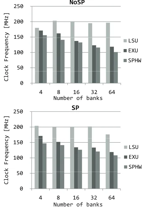
Fig. 8 shows the clock frequency reported by the ISE12.1. The SPHW shows the worst clock frequency. This is be-cause the critical pass resides on the pass from the DBRI to the multipliers in the EXU. The EXU hardware is gen-erated by the handel-C. Thus, this critical pass is depen-dent on the C program to be compiled by the handel-C. The LSU does not affect the clock frequency.
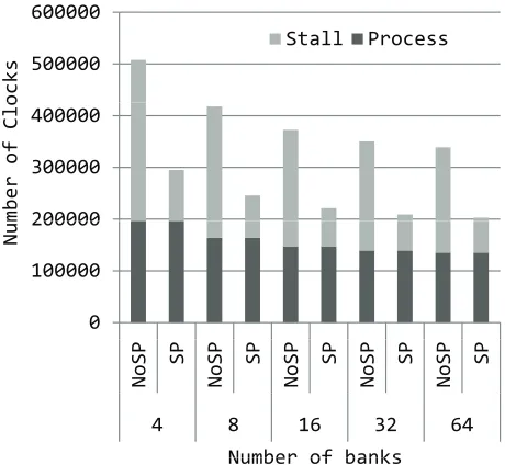
Fig. 9 shows the performance result when the line trans-fer from the memory to the LSU consumes 6 clocks. The image size is 256 × 256. By hiding memory access la-tency, the SP can improve the performance of 1.67 to 1.72 times compared with the NoSP.
We were able to perform such tradeoff among the num-ber of banks, the circuit size, the clock frequency, and the performance easily and quickly by only changing param-eters.
6
Conclusion
The semi-programmable hardware is a design-level hard-ware architecture residing on the pass of which C
pro-NoSP
2 0
NoSP
c y [ M H z ] 150 200 250 c k F r e q u e n c 50 100 150 LSU EXU SPHW
Numberofbanks
C
l
o
c
0
4 8 16 32 64
SP
200 250 y [ M H z ] 50 100 150 LSU EXU SPHW c k F r e q u e n c y 0 504 8 16 32 64
C
l
o
c
Numberofbanks Numberofbanks
Figure 8: Implementation Result (Clock Freq.).
gram with memory accesses is converted to hardware. The SPHW realizes the memory access controller and the buffer by writing the software program and parameters respectively.
In this paper, we have introduced the SPHW as the data processing hardware into a real commercial HLS tool, Handel-C. By using the SPHW providing the register-based data access interface, we have demonstrated that the HLS tool can easily write the hardware accessing to the memory in C. This is because this interface hides the detail of the memory devices and the memory access pat-terns, by providing the data processing hardware with the simple stream data. For hiding memory access latency, the simple software-pipelining is able to be applyed to the memory access program and the parameters of the buffer. Consequently, we can realize the data processing hardware with data-prefetching mechanism at the com-plete C-level design entry, with lower burden.
[image:5.595.310.542.73.408.2]o
c
k
s 500000 600000
Stall Process
m
b
e
r
o
f
C
l
o
200000 300000 400000
N
u
m
0 100000 200000
Numberofbanks
N
o
S
P
S
P
N
o
S
P
S
P
N
o
S
P
S
P
N
o
S
P
S
P
N
o
S
P
S
P
4 8 16 32 64
[image:6.595.56.286.71.283.2]Numberofbanks
Figure 9: Performance Result.
References
[1] Mentor Graphics. Handel-c synthesis methodology. http://www.mentor.com/products/fpga/handel-c/, 2010.
[2] Sumit Gupta, Nick Savoiu, Nikil Dutt, Rajesh Gupta, and Alex Nicolau. Using global code mo-tions to improve the quality of results for high-level synthesis. IEEE Trans.on Computer-Aided Design of Integrated Circuits and Systems, 23(2):302–312, 2004.
[3] David Lau, Orion Pritchard, and Philippe Mol-son. Automated Generation of Hardware Acceler-ators with Direct Memory Access from ANSI/ISO Standard C Functions. In IEEE Symp. on Field-Programmable Custom Computing Machines, pages 45–56, 2006.
[4] X. Liang and J. Jean. Data buffering and allocation in mapping generalized template matching on recon-figurable systems. The Journal of Supercomputing, 1(19):77–91, May 2001.
[5] Mitrionics.Mitrion Users’Guide 1.5.0-001. Mitrion-ics, 2008.
[6] J. Park and P. C. Diniz. Synthesis of pipelined mem-ory access controllers for streamed data applications on FPGA-based computing engines. InProc. of intl. symp. on Systems synthesis, pages 221–226, October 2001.
[7] D. Pellerin and S. Thibault. Practical FPGA Pro-gramming in C. Prentice Hall, 2005.
[8] S. P. Vanderwiel. Data Prefetch Mechanisms. ACM Computing Surveys, 32(2):174–199, 2000.
[9] Akira Yamawaki, Seiichi Serikawa, and Masahiko Iwane. An efficient hardware architecture from c program with memory access to hardware. InProc. of the 2010 International Conference on Computa-tional Science and Its Applications, Part II, pages 488–502, 2010.