Switching at Zero Voltage Level
Mr. Pratik Jejurkar1, Ms. Sapana Lokhande2, Mr. Aditya Mate3, Mr. Vaishnav Vijaykumar4, Dr. D. P. Kadam5 1, 2, 3, 4
B.E., Student, Dept. Of Electrical Engg MET BKC IOE, 5
Head of Department, Dept. Of Electrical Engg, MET BKC IOE
Abstract: The project is designed to develop a device to increase the life of equipment. For example, consider a resistive load as Incandescent lamps. They are having a property of very low resistance in cold condition. Due to which lamp circuit draws very high current at the time of switching, resulting into a fast failure of lamps. Random switching of lamps may occur at any instant of the sinusoidal voltage/current waveform. Assume switching is done at the peak value supply voltage. When such switching of the load (Incandescent Lamp) occurs and as the lamp is having low resistance in cold condition, then the current further shoots up. This will lead to premature failure of the lamp. The proposed project idea provides a solution for the current shoots in the circuit. This is done by connecting a TRIAC in circuit such that the controlling the firing angle of the TRIAC by detecting the zero cross point of the waveform of supply voltage and after switching of the lad is done. The project contains comparator here is ZVS (Zero Voltage Switching) which is given as reference interrupt to the microcontroller. Arduino microcontroller is used in this project idea.
Keywords: Arduino UNO, AC Voltage Regulator, Light Emitting Diode, LCD, capacitor.
I. INTRODUCTION
Random voltage switching operates like it states, it energizes the output switch whenever the timing circuit signals it to do so, meaning that the external load can turn on at any point in the AC voltage waveform.
An AC circuit changes polarity frequently. I India it changes 50 times per second, and generally written as 50Hz or even50 cps (cycles per seconds). This means that the voltage polarity changes from +/- to -/+ and back to +/- 50 times per second.
If switched is on at random instant suppose here at peak of voltage waveform the transients are created in the waveform which leads to formation of harmonics and leads to the damage of the equipment. To avoid this zero voltage circuit is developed. In the circuit the ZVS is used which is used to detect the zero crossing of the waveform and sends signal to the microcontroller. Microcontroller receives the signal and gives output signal to the opto-isolator.
II. IMPLEMENTATION SETUP COMPONENTS
A. Arduino Board
Arduino is a simple microcontroller board. It is based on an open-source physical computing platform. The Arduino Uno is a
microcontroller board based on the ATmega328 (Arduino Nano 3.x) or ATmega168 (Arduino Nano 2.x). It has 14 digital
[image:1.612.229.418.570.714.2]input/output pins. Out of these 14 pins, 6 pins can be used as a PWM output. 8 analog inputs, a 16 MHz crystal oscillator, a USB connection, a power jack, an ICSP header, and a reset button. It contains everything needed to support the microcontroller. USB cable is used for the connection of the Arduino Nano board to the computer or laptop. It is having 40 mA of DC current per I/O (Input Output) pin. It is having 16KB Flash memory in ATmega168 and 32KB Flash Memory in ATmega 328. The 2KB of the total Flash Memory is used by the Bootloader.
B. AC Voltage Regulator
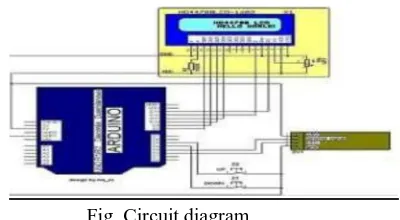
Fig. Circuit diagram
AC voltage regulator is also called as AC voltage controller. It is an electronic module. This electronic module is based on SCRs, TRIACs or IGBTs. These are used to convert a fixed voltage and fixed frequency of alternating current (AC). With this we get the variable output which is delivered to the load. The load in this project is resistive load. The working is in similar fashion of an autotransformer. AC voltage controller modules have high efficiency and low maintenance.
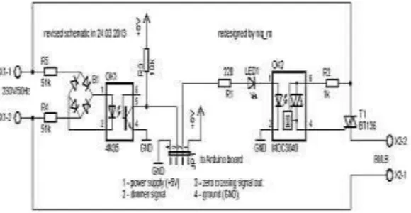
C. Zero Crossing Detector
A Zero Cross Detector or circuit operates on a AC waveform of a load voltage/current. It detects the zero crossing or 0 voltage of the AC sinusoidal waveform.
The main purpose of the circuit is to triggering the TRIAC at zero voltage level of the waveform, so that the output voltage is an complete half cycle.
[image:2.612.178.430.354.432.2] [image:2.612.217.438.576.718.2]The fig shows the circuit diagram and the waveforms of the Zero Voltage Crossing Detector.
Fig. Circuit Diagram of Zero Crossing Detector
Fig: Waveform of Zero Crossing Detector
D. Power Supply Block
The block diagram along with its circuit connections shows the conversion of single phase 50Hz AC to the 5V DC.
[image:3.612.203.447.114.214.2]1) Bridge Rectifier
Fig. Diode used in Rectifier
A diode bridge commonly known as bridge rectifier is an arrangement of four diodes in a bridge configuration. This configuration provides the output for either polarity of input. This is most commonly used in the application of AC to DC conversion. A bridge rectifier provides a full wave rectification for AC quantity.
[image:3.612.281.366.312.447.2]2) Opto-Isolator
Fig. Opto- Isolator
An opto-isolator contains a light source and photodiode. The LED (Light Emitting Diode) is used for the conversion of electrical energy into a light energy.it is having a closed optical channel and a photo sensor. Its function is to detect incoming light and either generates electric energy directly, or modulates electric current flowing from an external power supply.
III. WORKING MODEL
In this project, adjustment of lamp switching is done by connecting to the circuit through serial port. The brightness can be changed according to the commands provide to the serial port.
[image:3.612.180.470.551.701.2]Using these particular commands in this project, and design a Pulse Wave Modulated (PWM) dimmer circuit which will use in a full bridge rectifier. This full ridge rectifier output is used to control the voltage across the load(lamp). The rectifier used consist of an IN4007 diodes which are connected as shown in a diagram.
The diode D6, the load resistor R5, and the capacitor C2 connected as shown in figure. This forms a rectifier. From figure resistor R5 is a Positioning resistor. The function of the positioning resistor is that it limits the current pulses through diode D6 up to 1.5A. The opt coupler and the resistor R2 are used for driving the gate. Opto coupler contains LED which is protected by resistor R1. The opto coupler used is MCT2E. this opto coupler provides the class-2 isolation.
[image:4.612.156.457.180.387.2]IV. RESULT
Fig. Hardware Setup
A. Description of Hardware Setup
The figure shows the setup of hardware components of the circuit. The Arduino Nano type of controller is used. The LCD (Liquid Crystal Display) screen provided in the circuit. This screen shows the time in Microseconds. The time required for the switching is shown on the LCD screen.
LM 393 is a Comparator. It is a dual differential comparator. The pulsating DC is input given to the comparator (here is ZVS). The output of the comparator is given to the Arduino Nano controller. The digital input pin is used for the connection of the comparator output and Arduino Nano controller. The main function of the comparator is to generate the pulse as the zero crossing of the voltage is detected. As the zero crossing level of the voltage is detected, the comparator generates the pulse which is given to the Arduino Nano controller.
The MOC302 is used in the circuit of the TRIAC. The MOC302 is nothing but the opto- isolator. the working of the opto-isolator is as mentioned above. The input to the Opto- Isolator is given by Arduino Nano Controller. The output of the opto- isolator is given to the gate of the TRIAC. As opto- isolator gives signal or gate pulse the TRIAC starts conducting and the switching is done at zero voltage level.
For resistive load the TRIAC is used. The current is in phase with the voltage for the case of resistive load. For the load other than resistive load the rely is used for the switching of the RL type of load. This type of switching can be done for the three phase load also.
The voltage stabilizers are used in the circuits of the devices. The main function of the voltage stabilizer is to minimize the voltage swell and fill the voltage sag. The voltage sag is nothing but the missing voltage and swell is nothing but the increased in the voltage level from the nominal voltage level. The voltage sag and voltage swell are the main issues of the power quality. These major issues are avoided by this setup i.e. zero voltage switching.
The spike guard is also used in many circuits for protection of the electrical device. The main function of the spike guard is to suppress the voltage spike. Thus by switching the load at zero voltage level the spikes in the circuit are avoided.
V. ADVANTAGES
A. Reduced Inrush Current
In random switching of the equipment the inrush current is high. Switching or turning ON the equipment at Zero voltage reduces the inrush current considerably.
The reduction in inrush current has advantage that it extends the life of the equipment and also reduces the amount of EMI (Electromagnetic Interference) produced when turning on the load.
B. Reduced EMI & RFI
High inrush currents causes Electromagnetic Interference. This EM waves causes the improper operation of the sensitive electronics components.
RFI is a Radio Frequency Interference. The sudden change in the voltage level in a circuit leads t the formation of RFI. Therefore, the random switching leads to the formation of RFI, which causes high-frequency ringing which can also interfere with the operation of sensitive electronic equipment.
1) Construction of AC regulator is simple and compact.
2) External commutation circuits are not required.
3) Maintenance required is very less.
4) Running cost is also less.
5) Efficiency is high.
VI. DISADVANTAGES
A. In ON-OFF control strategy periodic power is sent to the load which influence load performance
B. In phase control strategy harmonics are produced in supply current because of non-sinusoidal load current
REFERENCES
[1] A review of Zero Voltage Switching and its importance to Voltage Regulation by Steven keeping Contributed by Electronic products (2014-08-05).
[2] Implementation of Arduino based AC Zero Voltage Switching for Electrical Equipment. International Journal of Engineering Research in Electrical and
Electronic Engineering (IJEREEE). Vol 4, Issue 2, February 2018.
[3] Ma Huasheng, Zhao Liang, Zhang Bo, Zheng Jianchao.:‘AC/AC Buck Converter Instantaneous Value Control Modeling, System Analyzing and Designing’,
Proc. of the IEEE Electrical Machines and Systems Conference, Nanjing, Sept 2005, 2, pp. 1391 – 1395
[4] Rosas-Caro, J.C., Mancilla-David, F., Ramirez-Arredondo, J.M., Bakir, A.M.: ‘Two-switch three-phase ac-link dynamic voltage restorer’, IET J. Power
Electronics, 2012, 5, (9) , pp. 1754-1763.
[5] Jothibasu, S., Mishra, M.K., ‘An Improved Direct AC–AC Converter for Voltage Sag Mitigation’, IEEE Transactions on Industrial Electronics, 2015, 62, (1),