Faculty of Electrical Engineering,
Mathematics & Computer Science
Control Surface Waves by
Modifying Surface Properties
of a
Microstrip Patch Antenna Array
Stephan de Louw MSc. Thesis
April 2017
Supervisors Daily
dr. ir. G. H. C. van Werkhoven MSc. D. Alvarez Menendez
Supervisors Committee
Not publicly accessible.
Summary iii
List of Abbreviations vii
1 Surface Waves; an Introduction 1
1.1 Intro . . . 1
1.2 Background . . . 1
1.2.1 Surface Waves in Microstrip Patch Antenna Array . . . 1
1.2.2 Surface Wave Model . . . 4
1.2.3 Surface Waves Reduction . . . 9
1.3 Investigation Goals . . . 16
1.4 Report organization . . . 16
2 Reducing Surface Waves; a Theoretical Approach 17 2.1 Coupled Free-Space - Surface Impedance TL Model . . . 17
2.1.1 Air-Grounded Dielectric Slab . . . 17
2.1.2 Air-Patch-Grounded Dielectric Substrate . . . 17
2.1.3 Air-Patch-Via-Grounded Dielectric Substrate . . . 17
2.2 Composite Right/Left-Handed TL Model . . . 17
2.2.1 1-D CRLH∆z→0 . . . 18
2.2.2 1-D CRLH∆z→D . . . 18
2.3 HFSS Eigenmode Solver . . . 18
2.3.1 HFSS Limitations . . . 18
3 EBG Concept Design and Validation Theoretical Models 19 3.1 EBG Concept Design . . . 19
3.2 Validation Theoretical Models . . . 19
3.2.1 HFSS Eigenmode Solver . . . 19
3.2.2 COF-SIM TL Model - HFSS Eigenmode Comparison . . . 19
3.2.3 CRLH TL Model - HFSS Eigenmode Comparison . . . 19
4 Reducing Surface Waves; a Practical Environment 21
4.1 Mutual Coupling Reduction Between Antenna Elements . . . 21
4.1.1 HFSS MC Simulation Model . . . 21
4.1.2 HFSS MC Results . . . 21
4.2 Edge Surface Wave Reduction . . . 21
4.2.1 TM Waves and Edge SW Reduction . . . 21
4.2.2 TE Waves and Edge SW Reduction . . . 21
4.2.3 Edge SW Reduction Conclusion . . . 21
5 Conclusions and Recommendations 23 5.1 Conclusions . . . 23
5.2 Recommendations . . . 24
References 25 Appendices A Derivation Directional Impedance for Via Medium 31 B Derivation Valid Regions COF-SIM Model 33 C Notes on HFSS Eigenmode Solver 35 C.1 Height Variation . . . 35
C.2 Mode Inspection . . . 35
D HFSS Model Composite Right/Left-Handed Model 37 E Reducing Surface Waves; a Practical Environment, extending plots 39 E.1 0.8f /fn . . . 39
E.2 1.1f /fn . . . 39
E.3 1.3f /fn . . . 39
E.4 TE Electric Vector Field plot . . . 39
E.4.1 0.8 f /fn . . . 39
E.4.2 1.1 f /fn . . . 39
AF Array Factor
CRLH Composite Right/Left-Handed
COF-SIM Coupled Free-Space - Surface IMpedance
EBG Electromagnetic Band Gap
FSS Frequency-Selective Surfaces
HIS High-Impedance Surface
HFSS High Frequency Structure Simulator (product name)
LW Leaky Wave
PCB Printed Circuit Board
PW Plane Wave
RF Radio Frequency
SW Surface Wave
TL Transmission Line
TM Transverse Magnetic
Surface Waves; an Introduction
1.1 Intro
This research is done as the final part of the master Electrical Engineering studied at the University of Twente. The research is done externally at Thales Netherlands, at the branch located in Hengelo, responsible for naval, logistics, and air defence systems. Most of there systems rely on radar, and therefore this thesis is also con-nected to radar systems.The thesis investigates a very small part in the whole radar system and focuses on the antenna panel consisting of microstrip patch antennae. One of the possible ways to improve the antenna patterns of the radar is by the re-duction of the interferences causes in the patterns by Surface Waves (SWs). In this project a solution is investigated for aX-band system (8.0−12.0GHz), although the
theory is applicable for different frequencies.
This chapter, Chapter 1, gives some background information about SWs, how they can be reduced and the chapter ends with the report organization.
1.2 Background
1.2.1 Surface Waves in Microstrip Patch Antenna Array
Nowadays many radar systems are based on array antennas since they have clear benefits over classical (reflectors) based systems. For example fast electric beam steering and adaptivity of the used beam shapes. In one array antenna, the an-tenna pattern is not formed by a single radiating element but by the coherent com-bination of all elements in which weighting factors can be applied. These factors enables beam steering and/or beam shaping.The resulting antenna beam pattern is (to some degree of accuracy) given by the Array Factor (AF) multiplied with the aver-aged element pattern. By using certain weigh factors for each element an antenna
pattern is created which is suitable for a radar application, with a main lobe and low side lobes. Unfortunately the side lobes have still enough energy and under some conditions they are able to propagate along the surface, known as surface waves. Since surface waves are propagating waves, propagating along a surface, they can increase the coupling of energy between array elements, so called mutual coupling. Mutual coupling is an unwanted limiting factor of array antennas, affecting its radi-ation pattern and scan behaviour. But this is not the only problem, the SW also brings Radio Frequency (RF) power to the antenna’s panel edge. When the edge is reached it starts to re-radiate in the same plane as the radiation occurs. The fields from the edge add up constructive or destructive with the primary element pattern. These effects are shown in the coming part.
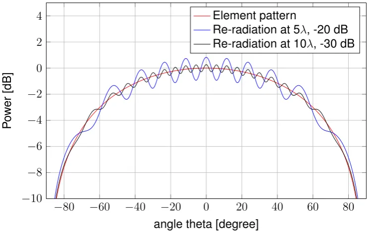
Figure 1.1 shows the case where a single element is transmitting and an additional source represents the panel’s edge. This additional source is located at 5λ, power
−20dB with respect to the primary element, and10λ,−30dB and add up destructive
(90°degree out of phase).
From the Figure a trend is visible, less power for the additional source leads to a smaller ripple compared to single element pattern. Further power decreasing lead to a negligible effect on the main element pattern. This is the case for a single element and edge radiation. However in an antenna array each element has a different distance to the edge and so the interference is different. This can cause element patterns in the array and change the array beam pattern.
−80 −60 −40 −20 0 20 40 60 80 −10 −8 −6 −4 −2 0 2 4
angle theta [degree]
Po
w
er
[dB]
Element pattern
Re-radiation at 5λ, -20 dB
[image:10.595.100.474.465.699.2]Re-radiation at 10λ, -30 dB
Figure 1.1 shows the influence on one element but does not show the impact on the radiation pattern in a linear 1D array. AssumeN elements with an inter element
spacing equal tod1. Without the re-radiation the field pattern expressed in power is
represented by [1]:
P (θ) =
N X
n=1
wnej(n−1)(kd1cosθ+β)
∗fe(θ) (1.1)
wherewnis weighting factor that depends on the element,krepresents the
wavenum-ber,θthe scan angle,βis the phase different between the elements andfe(θ)is the
radiation pattern of a single element. Due to the re-radiation an additional term is required:
P (θ) =
N X
n=1
wnej(n−1)(kd1cosθ+β)∗fe(θ) +wswej(n−1)(k(d1+d2) cosθ+β) (1.2)
whered2is the additional distance seen from then-th inspected element toward the
location where the re-radiation occurs and is responsible for an additional phase change. The weighting functionwsw is:
wsw =κejkd2 (1.3)
whereκ is a constant, representing the amplitude of the SW. Concluded each
indi-vidual element pattern is affected by re-radiation, and so the total radiation pattern is influenced. When the re-radiated power becomes stronger the interference level is increased.
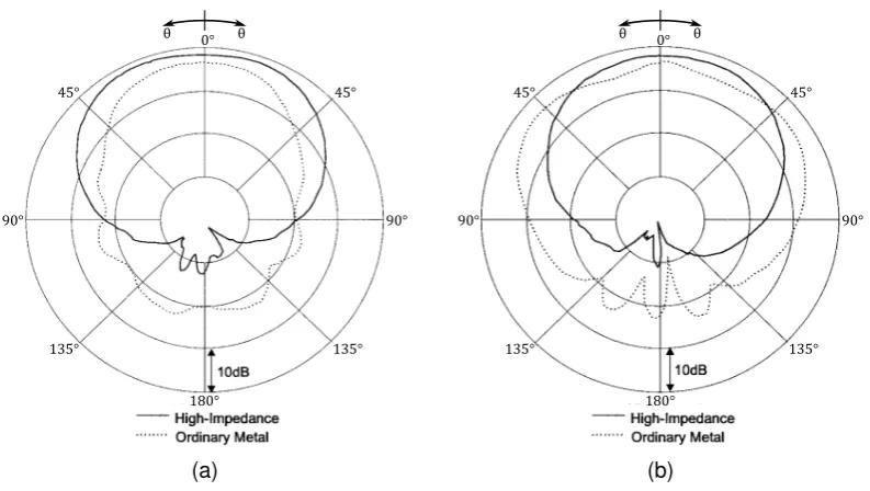
In the previous part the effects of SWs on the element pattern was addressed and some first steps were made to a 1D array. The coming part extends this part and show the radiation pattern for two radiating patch antennas and the effect of SWs. Sievenpiperet al.[2] measured the radiation pattern for two radiating elements and
changes the surfaces to affect SWs. The first surface consist of a metal plane (con-ducting) where the second surface is made from a materiel that creates a high-impedance surface. The high-high-impedance surface does not support SW propagation and so no re-radiation occurs. The used configuration is shown in Figure 1.2.
[image:11.595.94.531.657.707.2](a) (b)
The resulting radiation patterns are shown below. 0° 45° 90° 135° θ θ 45° 90° 135° 180° (a) 0° 45° 90° 135° θ θ 45° 90° 135° 180° (b)
Figure 1.3: (a) H- and (b) E-plane radiation patterns of patch antennas on two dif-ferent ground planes.
In Figure 1.3 is seen that for an ordinary metal plane significant radiation occurs in backward direction 90◦ < θ < 180◦. The forward direction, 0◦ < θ < 90◦, shows
for the metal plane different behaviour in the H- and E-plane. A narrow radiation pattern in the H-plane and a broader pattern in the E-plane. The metal depends on the polarisation. This makes the radiation pattern non rotationally symmetry.
The High-impedance surface shows different behaviour. SW are not able to prop-agate along the surface, and no radiation occurs at the panels edge. Both planes are symmetric and the radiation patterns becomes smoother. The backward ration is almost reduced and the forward radiation improved.
Concluded SW reduction improves the radiation pattern because energy is not re-radiated any more. Panel’s edges or objects in the surrounding area have less influence on the element patterns. Different radome fixation can be used or other objects can be placed closer by.
1.2.2 Surface Wave Model
assuming incident TM waves under one specific angle (Brewster angle). They did not give a general description of a SW. In 1960 Balow [5] came with a SW definition:
"A surface waveis one that propagates along an interface betweentwo different
media without radiation, such radiation being construed to mean energy converted from the surface-wave field to some other form."
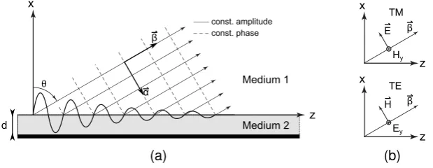
This definition describes how a surface wave looks like, but it is not a mathematical description. In the coming section a SW is expressed as a mathematical expression. A description of SW starts from Figure 1.4 and by solving Maxwell’s equations in the transition region. Assume the SW propagates into thez-direction (Figure 1.4a),
po-larisation (Figure 1.4b independent). A general description starts from the complex plane wave solution. This means the propagation constant is complex and has an attenuation constant per unit distance depended of direction α, and a propagation
constant, representing the change in phase per unit length depended of direction,
β. The total complex propagation constant becomesγ =α+jβ. It is assumed all
solutions have a time-harmonic dependency (ejωt).
x
d Medium 2
[image:13.595.160.470.394.514.2]Medium 1 z y θ β const. amplitude const. phase θ β α (a) x z Ey H TE β x z Hy E TM β (b)
Figure 1.4: (a) General TM and TE leaky surface wave, propagating intoz-direction,
(b) Polarisation definition.
For now consider only the field in Medium1for which the electric field can be written
as:
TM TE
Ey = 0 (1.4)
Ex,z(x, z) =E0e−γzze−γnx (1.5)
=E0e−αzz−jβzze−αnx−jβnx (1.6)
Ex =Ez = 0 (1.7)
Ey = jωµ0
γn H0e
−γzze−γnx (1.8) Ey = jωµγn0H0e−αzz−jβzze−αnx−jβnx (1.9)
whereγzdescribes the propagation along the surface andγnthe propagation normal
to the surface. When α = 0 the amplitude stays constant for a phase front. This
interaction with a different medium. For the opposite case, α 6= 0 the amplitude
varies over the phase front (inhomogeneous wave, leaky wave or surface wave). Assume a TM polarization and substituting Equation 1.5 into Equation 1.10, known as Helmholtz equation, assuming free space
∂2E
∂x2 +
∂2E
∂y2 +
∂2E
∂z2 +k 2
0E = 0 (1.10)
using separation of variables [6], gives a dispersion relation:
γ2
z +γn2+ω2(0µ0) = 0 (1.11)
β2
z +βn2−(α2z +α2n)−2j(αzβz+αnβn) = ω2(0µ0) (1.12)
and splitting Equation 1.12 into a real and imaginary part:
Re→β2
z +βn2 −(αz2+αn2) =ω2(0µ0) =k02 → |β|
2− |α|2 =k2
0 (1.13a)
Im→ −2(αzβz +αnβn) = 0 →α·β= 0 (1.13b)
For a Plane Wave (PW) αn =αz = 0and β 6= 0, and therefore only Formula 1.13a
exists. On the other hand, complex travelling waves (inhomogeneous waves), have
α6= 0 and both Formulas 1.13a and 1.13b hold.
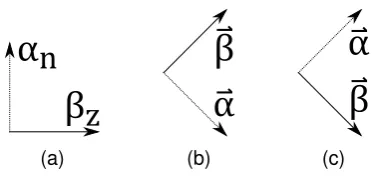
SWs are inhomogeneous waves, αn 6= 0, αz = 0, combining with Figure 1.4a gives
the components ofα, andβ. A bounded SW has a phase constant along the surface
and the attenuation constant normal to the surface pointing into the positive direction (Figure 1.5a). Unbounded waves, Leaky Waves (LWs), will ’leak’ from the surface, and therefore the phase constant is pointing into free-space and has an attenuation constant pointing into the surface (Figure 1.5b). Theαnbecomes negative, resulting
in an infinite field inx-direction and an attenuated field intoz. It is pure a theoretical
description of a LW and is not possible in reality. Interchanging the α and β from
the LW creates a new type of wave, known as the Zenneck SW (Figure 1.5c). This wave shows opposite behaviour compared to the LW. The wave propagates into the substrate and due to the positive α the wave shows exponential decay. In fact the
Zenneck SW is a SW that decays.
All the different configurations are given in the tabular below. Wave type α β
PW α= 0 β6= 0
LW α6= 0 β6= 0
β
z
α
n
(a)α
β
(b)α
β
(c)Figure 1.5: (a) Surface Wave, (b) Leaky Wave, (c) Zenneck Surface Wave.
So far, the focus was only on Medium 1 and for this layer the corresponding wave
numbers were explained. But SWs, can only exists in the presence of two mediums, as part of its own definition. The combination of the field in both media determine SW propagation. Therefore the fields in Medium2are involved into the calculation.
Solving Maxwell’s equations in the transition region imposes the continuity of the tangential field components.
H1y x=0
= H2y (1.14) E1z
x=0
= E2z (1.15)
As consequences of the field continuity, the impedances are also equal use equal and therefore the transverse resonant condition [7] is valid. This means the situation can be modelled with an equivalent transmission line circuit, where both media are represented by a transmission line.
z x
εrε0,μrμ0 ε0,μ0
d
(a)
z x
Dielectric
Air βn1, Zair
βn2, Zslab
d
(b)
Figure 1.6: (a) x < 0, Dielectric slab, thickness d, and x > 0 air, (b) transverse
resonance equivalent circuit, from Pozar [7].
The impedance sign depends on the direction of viewing (Zx=0 = +or−). For
ex-ample by looking towards Medium1fromx = 0gives a positive impedance, and so
[image:15.595.152.475.541.642.2]Z1x=0 =
E1z H1y ↔
E2z H2y
=−Z2x=0 (1.16)
Z1x=0(γn1) =−Z2x=0(γn2) (1.17)
Z1x=0(γn1) +Z2x=0(γn2) = 0 (1.18)
The transverse resonant condition it self does not tell anything about SW propaga-tion. For predicting SWs an additional condition is imposed from solving Maxwell’s equations also known as Snell’s law and is:
γz1 =γz2 (1.19)
which links the propagation into thez-direction in both media. Whit Equations 1.17
and 1.19 a prediction can be made about SW propagation. The equations are changed by assuming SW propagation.It starts by expressing Z2x=0(γz) in
Equa-tion 1.17 to a propagaEqua-tion constant in z-direction. Equation 1.11 is used for this
propagation transformation but with the corresponding materials properties and be-comes:
γ2
z +γn2 +µrrk02 = 0 (1.20)
Furthermore the impedance of medium 1 (air) is known and so Equation 1.17 can
be rewritten to:
γn1 =Z2x=0(γz2;f req) (1.21)
Equation 1.20 is used again for expressingγn1 towardsγz1 (µr=r = 0):
γz1 =
q k2
0−γn21γz1 =
q k2
0−(Z2x=0(γz2;f req))2 (1.22)
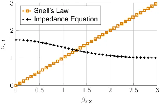
This function shows a function whereγz1depends onγz2. However according
0 0.5 1 1.5 2 2.5 3 0
1 2 3
βz 2
βz
1
Snell’s Law
[image:17.595.177.452.89.268.2]Impedance Equation
Figure 1.7:Plotted dispersion equations for one frequency.
1.2.3 Surface Waves Reduction
In order to modify or attenuate SW propagation, the SW should be expressed in both mediums by using the transverse resonant conditions. For using the transverse res-onant condition, Equation 1.18, the impedances of both mediums should be known. Medium 1 is assumed to be air and the impedance is derived in Appendix A for
[image:17.595.245.381.499.595.2]both polarizations and replaceβnwith a complex propagation constant−jγn, where γn =αn+jβn, for angle of incidence and independent of polarisation. According to
Figure 1.8 a SW propagates intoz and soβn= 0. x
z Zs= Rs + jXs
Zs= Rs + jXs βz
αn
Figure 1.8: Illustration of a plane impedance surface, with propagating SW.
The other Medium, Medium2, can be a dielectric slab, a periodic complicated
struc-ture, as long as the period is small compared to the wavelength, or any other mate-rial. In these cases the surface is approachable by an equivalent surface impedance,
Zs=Rs+jXs. Furthermore the assumption is made that Medium2is independent
of polarisation or angle of incident.
ZT M air = −jγn
ω0
SW
→ −jαn1
ω0
(1.23)
ZT E air = ωµ0
−jγn =ωµ0
(βn1+jαn1)
β2
n1 +α2n1
SW
→ jωµ0
αn1
(1.24)
Substituting Equation 1.23 and Equation 1.24 in Equation 1.18, and assumingZs n = Rs+jXs.
ZT M =−ZsT M
−jαn1
ω0
=−Zs=−Rs−jXs (1.25)
ZT E =−ZsT E jωµ0
αn1
=−Zs=−Rs−jXs (1.26)
From both equations, Equation 1.25 and Equation 1.26 is concluded that changing the imaginary part controls the normal attenuation constant, or in other words it determines how closely the SW is bound to the surface. Furthermore from these two equations it is seen that the sign of the imaginary part also contains SW propagation information. Equation 1.25 shows that for TM SW propagation the imaginary part should be positive. In contrast to Equation 1.26 that shows for TE SW propagation the imaginary part should be negative.
The propagation intoz-direction is calculated from Equations 1.23 and 1.24 in
com-bination with the wave number equation:
k2 0 =γ
2
n1+γ 2
z1 (1.27)
where γ = −j(α+jβ). For a pure SW the complex propagation constant into
z-direction only depends on βz and α = 0 and so the propagation into z-direction
−jαz1T M +βz1T M = q
k2
0 −ω220(R2s−Xs2+ 2RsXsj) (1.28) βz1T M SW=
q k2
0−ω220(R2s −Xs2) (1.29)
−jαz1T E +βz1T E = s
k2 0 +
ω2µ2 0
R2
s−Xs2+ 2RsXsj
(1.30)
βz1T E SW= s
k2 0+
ω2µ2 0
R2
s−Xs2
(1.31) Theβz component is linked to the relation R2
s −Xs2. When Rs < Xs, βz is real and
therefore the wave is bound to the surface. In the other scenario, whenRs> Xs,βz
becomes imaginary and the wave propagates away from the surface (leaky wave). For TM waves the same conclusion is found by Collin [8]. He assumes a normalized surface impedance with respect to the intrinsic impedanceZ0. Furthermore he
in-vestigated only TM polarisation since naturally occurring surfaces have an inductive reactive term in the surface impedance. Hence, TM surface waves are more com-mon than TE SWs. His explanation is used to create a graphical representation, starting from an incident TM wave, Figure 1.9. From the resulting figures it can be seen what the effect is of the surface impedance on the SW propagation.
x
z Zs= Rs + jXs
Zs= Rs + jXs Ex
Ez Hy
[image:19.595.176.524.104.235.2]Constant phase plane
Figure 1.9:Illustration of a plane impedance surface, with a TM surface wave. The magnetic field in the top part (x >0) is expressed as:
Hy =Ae(jγnx−jγzz) (1.32)
whereγ2
n+γz2 =k20 and the electric field components are given by:
jω0Ez = ∂Hy
∂x (1.33)
jω0Ex =−
∂Hy
∂z (1.34)
and from which the wave impedance is found:
ZT M = EZ
Hy = γn ω0
= γn
k0
By using the transverse resonant condition he find the same surface wave depen-dency as function of the surface impedance.
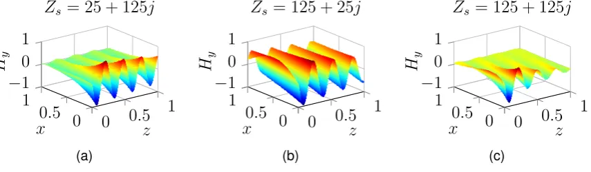
In Figure 1.10 the magnetic field component is inspected for different surface impedances.
0 0.5 1 0
0.5 1 −1 0 1 z x Hy
Zs = 25 + 125j
(a)
0 0.5 1 0
0.5 1 −1 0 1 z x Hy
Zs = 125 + 25j
(b)
0 0.5 1 0
0.5 1 −1 0 1 z x Hy
Zs = 125 + 125j
[image:20.595.74.502.167.292.2](c)
Figure 1.10: Different surface impedances and the impact on a TM propagating SW. The first conclusion from Figure 1.10 is that a positive imaginary part supports a TM SW. The same was predicted with Equation 1.25.
Furthermore when Figure 1.10a is compared to Figure 1.10b it is noticed that fore a bound SW should hold Rs < Xs. This was already found by using Equation 1.29.
In Figure 1.10c an attenuated SW is shown. This can not explained by neither Equation 1.25 nor Equation 1.29 because the assumption was made a pure SW is present. For an attenuated SW an attention factor is needed and Equation 1.28 should be used. The productRsXsdetermines the attenuation. For Figure 1.10c the
product is larger compared to Figure 1.10a and Figure 1.10b. This means the wave is more attenuated. In addition Figure 1.10c shows Rs = Xs. From the colour it is
seen that Hy is stronger at x= 1, y = 0andz = 0 compared to Figure 1.10a where
Rs< Xs. This means a small part radiates from the surface.
Concluded changing the surface impedance affects the propagation properties. For SW reduction the surface should have a high real part and a small imaginary part and/or the productRsXs should be large. Although increasing the real part might be
a proper solution, it is better to change the imaginary part. The real part absorbs the wave’s energy, which results into head at unwanted places. Furthermore the transmitted signal is produced with a lot of costly components and energy absorbing is waste of energy. Changing the imaginary part effects the bounding conditions. A lossless bounded SW propagates into free space and it is the preferred method. Changing the imaginary part only, is not straightforward. A metallized surface has a surface impedance [8]:
Zs=Z0(1 +j)
r γ0
2σZ0
where the real part can not be changed independent of the imaginary part. Further-moreσ is for metals large (order of107 [9]) and so the real and imaginary parts are
small, leading to a unbound, less attenuated TM SW.
Another possibility is a grounded dielectric surface. The surface impedance are derived in Appendix A and the results is given below:
Zs T M = γn2
ωr0
jtan (γn2d) (1.37)
Zs T E =
ωµrµ0
γn2
jtan (γn2d) (1.38)
whered is the substrate’s thickness. The tan functions is responsible for a flipping
sign as function of frequency and the substrate’s thickness, supporting TM and TE SWs. Yakovlev et al. [10] derived a frequency-wavenumber diagram, also known
as dispersion diagram. Such diagram shows for which frequency propagation is possible. The used slab thickness is 1 mm and a permittivity is used of = 10.2.
The found dispersion diagram is shown in Figure 1.11. For every wavenumber there exists a frequency and so SWs are always present.
0 5 10 15 20 25 30 35
0.5 1 1.5 2 2.5
[image:21.595.157.469.407.613.2]SW LW f [GHz] βz /k0 TM TE
Figure 1.11: Dispersion diagram for a grounded dielectric slab. Design is created by Luukkonenet al.[11].
All modes in Figure 1.11 start fromβz/k0 >1. The reason for this is the SW
assump-tion, the wave decays exponentially into the normal direction. This is only possible forβnvalues that are imaginary:
βn=k0
q
1−β2
Cases whereβz/k0 <1do exist, known as LW. In Subsection 3.2.4 LWs are shortly
addressed but this area does not belong to the major area of interest.
Unfortunately, the current surfaces do not contain a region where no SW can prop-agate. Especially this kind of behaviour is wanted. In literature different examples can be found for changing the surface impedance:
• Corrugations: varying thickness and material properties of a grounded dielec-tric slab. When the thickness is changed many times within a periodp(p << λ)
the surface can be represented with a surface impedance and is known as a corrugated surface [3], [12]–[15]. Also variations are possible where the corru-gation behaves like a cavity [16].
• Placing hemispherical structures on top of the surface. The radius and spacing between the centres are small compared to the wavelength. These structures are made from a different material (, µ, σ) and are uniform distributed on a
conducting surface [17]
• Electromagnetic Band Gap (EBG) surfaces also known as Frequency-Selective Surfaces (FSS) that form High-Impedance Surface (HIS) [18], [19]. These structures can be placed in one plane (xy-plane, uniplanar) or in multiple
planes (xy,xz planes, multiplanair). A broad variety is available for
unipla-nar structures starting from metallic uniform lines to more complicated struc-tures [20]–[23]. Also many strucstruc-tures are known for multiplanar configura-tions [24]–[27] but are a variation of the well known mushroom structures in-vented by Sievenpiper [28].
Especially the last one, EBG surfaces, is the preferred method because: firstly, the fabrication steps can easily be included into current Printed Circuit Board (PCB) fabrication steps. Secondly, the antenna panel remains perfectly flat, and last, the thickness/height needed to be effective is less compared to a corrugated surface (λ/
2).
Therefore this investigation focuses on changing the surface impedance by placing structures in/on top of the surface. Although uniplanar structures show band gap regions, multiplanar structures show a larger bandwidth for the band gap [29] and so these structures are preferred.
Figure 1.12: Sievenpiper mushroom structure, integrated into a grounded dielectric slab, metal parts are coloured grey.
Sievenpiper et al. [2] described the mushroom structure with a capacitor and an
inductor shown in Figure 1.13a and derived a simple impedance equation:
Z = jωL
1−ω2LC (1.40)
The surface is inductive at low frequencies and capacitive at high frequencies and gives a resonant frequency:
ω0 =
1 √
LC (1.41)
and by inspecting the reflection phase shift for different frequencies reveal the sur-face behaviour, shown in Figure 1.13b.
C L (a) Reflection3P hase3[radi ans] Frequency3[GHz] π/2 π 0
-π/2
π
0 5 10 15 20 25 30
Resonan
t
Frequ
ency
(b)
Figure 1.13: (a) Sievenpiper mushroom representation, (b) reflection phase of the high-impedance surface [2].
Different models are available that describe mushroom structures and there corre-sponding effective surface impedance. All the models related the frequency to the corresponding wave number and so it reveals the wave propagation properties into a specific direction (dispersion diagram). The models are:
[image:23.595.127.492.442.595.2]extend this idea to periodic structures, for example research done by Rah-man and Stuchly [30] and Caloz and Itoh [31]. They use a different name for their models known as Composite Right/Left-Handed (CRLH) Transmission Line (TL) model.
• Impedance representation of each individual layer. A total surface impedance is created by the combination of each individual impedance representation. Yakovlevet al.[10] explain this method. This method is known in this thesis as
Coupled Free-Space - Surface IMpedance (COF-SIM) TL model.
• Full wave electromagnetic simulations with a software suite like Ansys High Frequency Structure Simulator (HFSS). The possibilities of SW prediction are shown by Raza [32].
1.3 Investigation Goals
The goal of this investigation is to find out how SWs can be reduced using the mush-room structure. Different theoretical models are investigated and validated using An-sys HFSS simulations. One of the theoretical models is used to design a mushroom that has band gap in the wanted region. Furthermore, having a proper design, the structure is investigated in two scenarios. In the first scenario the mushrooms are placed in between the patch antennae to find out if the mutual coupling is effected. The second scenario is when the structure is placed in the available free space, that is formed by the outer row of the array antenna and the antenna panel’s edge.
1.4 Report organization
Reducing Surface Waves; a
Theoretical Approach
Not publicly accessible, only chapter names are given.
2.1 Coupled Free-Space - Surface Impedance TL Model
2.1.1 Air-Grounded Dielectric Slab
Dispersion Equation
2.1.2 Air-Patch-Grounded Dielectric Substrate
βz Direction Limitations
Impedance: Grid Dispersion Equation
2.1.3 Air-Patch-Via-Grounded Dielectric Substrate
Directional Permittivity
Modelling Directive Permittivityxx
Vias Frequency Dependency Via Medium Impedance Dispersion Equation
2.2 Composite Right/Left-Handed TL Model
2.2.1 1-D CRLH
∆
z
→
0
2.2.2 1-D CRLH
∆
z
→
D
2.3 HFSS Eigenmode Solver
EBG Concept Design and Validation
Theoretical Models
3.1 EBG Concept Design
3.2 Validation Theoretical Models
3.2.1 HFSS Eigenmode Solver
HFSS Eigenmode Settings Transition Region
3.2.2 COF-SIM TL Model - HFSS Eigenmode Comparison
3.2.3 CRLH TL Model - HFSS Eigenmode Comparison
3.2.4 Leaky Wave Region Investigation
Reducing Surface Waves; a Practical
Environment
4.1 Mutual Coupling Reduction Between Antenna
El-ements
4.1.1 HFSS MC Simulation Model
4.1.2 HFSS MC Results
4.2 Edge Surface Wave Reduction
4.2.1 TM Waves and Edge SW Reduction
4.2.2 TE Waves and Edge SW Reduction
4.2.3 Edge SW Reduction Conclusion
Conclusions and Recommendations
5.1 Conclusions
[1] C. A. Balanis, Antenna theory: analysis and design, 3rd ed. John Wiley &
Sons, 2005, ch. 6, pp. 290–296.
[2] D. Sievenpiper, L. Zhang, R. F. J. Broas, N. G. Alexopolous, and E. Yablonovitch, “High-impedance electromagnetic surfaces with a forbidden frequency band,” IEEE Transactions on Microwave Theory and Techniques,
vol. 47, no. 11, pp. 2059–2074, Nov 1999.
[3] H. M. Barlow and A. L. Cullen, “Surface waves,” Proceedings of the IEE
-Part III: Radio and Communication Engineering, vol. 100, no. 68, pp. 329–341,
November 1953.
[4] S. Schelkunoff, “Anatomy of "surface waves",” IRE Transactions on Antennas
and Propagation, vol. 7, no. 5, pp. 133–139, December 1959.
[5] H. E. M. Barlow, “Surface waves: a proposed definition,” Proceedings of the
IEE - Part B: Electronic and Communication Engineering, vol. 107, no. 33, pp.
240–, May 1960.
[6] D. Pozar,Microwave Engineering, 4th ed. Wiley, 2011, ch. 1, pp. 20–23.
[7] ——,Microwave Engineering, 4th ed. Wiley, 2011, ch. 3, pp. 153–154.
[8] R. Collin, I. Antennas, and P. Society, Field theory of guided waves, ser. The
IEEE/OUP Series on Electromagnetic Wave Theory (Formerly IEEE Only), Se-ries Editor SeSe-ries. IEEE Press, 1991, ch. Surface Waveguides, pp. 697–708. [9] C. A. Balanis,Advanced engineering electromagnetics. John Wiley & Sons,
1989.
[10] A. B. Yakovlev, M. G. Silveirinha, O. Luukkonen, C. R. Simovski, I. S. Nefe-dov, and S. A. Tretyakov, “Characterization of surface-wave and leaky-wave propagation on wire-medium slabs and mushroom structures based on local and nonlocal homogenization models,” IEEE Transactions on Microwave
The-ory and Techniques, vol. 57, no. 11, pp. 2700–2714, Nov 2009.
[11] O. Luukkonen, A. B. Yakovlev, C. R. Simovski, and S. A. Tretyakov, “Compara-tive study of surface waves on high-impedance surfaces with and without vias,”
in2008 IEEE Antennas and Propagation Society International Symposium, July
2008, pp. 1–4.
[12] A. F. Harvey, “Periodic and guiding structures at microwave frequencies,” IRE
Transactions on Microwave Theory and Techniques, vol. 8, no. 1, pp. 30–61,
January 1960.
[13] M. N. M. Kehn, “Rapid surface-wave dispersion and plane-wave reflection anal-yses of planar corrugated surfaces by asymptotic corrugations boundary con-ditions even for oblique azimuth planes,” IEEE Transactions on Antennas and
Propagation, vol. 61, no. 5, pp. 2695–2707, May 2013.
[14] C. Mentzer and L. Peters, “Properties of cutoff corrugated surfaces for corru-gated horn design,” IEEE Transactions on Antennas and Propagation, vol. 22,
no. 2, pp. 191–196, Mar 1974.
[15] R. Elliott, “On the theory of corrugated plane surfaces,”Transactions of the IRE
Professional Group on Antennas and Propagation, vol. 2, no. 2, pp. 71–81, Apr
1954.
[16] C. Molero, R. Rodriguez-Berral, F. Mesa, and F. Medina, “Analytical circuit model for 1-d periodic t-shaped corrugated surfaces,” IEEE Transactions on
Antennas and Propagation, vol. 62, no. 2, pp. 794–803, Feb 2014.
[17] J. Wait, “Guiding of electromagnetic waves by uniformly rough surfaces : Part
i,” IRE Transactions on Antennas and Propagation, vol. 7, no. 5, pp. 154–162,
December 1959.
[18] F. Yang and Y. Rahmat-Samii,Electromagnetic band gap structures in antenna
engineering. Cambridge university press Cambridge, UK, 2009.
[19] R. Garg, P. Bhartia, I. Bahl, and A. Ittipiboon, Microstrip antenna handbook,
2001.
[20] S. Keyrouz, G. Perotto, and H. J. Visser, “Lumped-elements tunable frequency selective surfaces,” inThe 8th European Conference on Antennas and
Propa-gation (EuCAP 2014), April 2014, pp. 475–478.
[21] F. Costa, S. Genovesi, A. Monorchio, and G. Manara, “A circuit-based model for the interpretation of perfect metamaterial absorbers,”IEEE Transactions on
[22] B. A. Munk,Finite antenna arrays and FSS. John Wiley & Sons, 2003.
[23] ——,Frequency Selective Surfaces: Theory and Design. Wiley Online Library,
2000.
[24] H. N. B. Phuong, H. V. Phi, N. K. Kiem, D. N. Dinh, T. M. Tuan, and D. N. Chien, “Design of compact ebg structure for array antenna application,” in 2015
In-ternational Conference on Advanced Technologies for Communications (ATC),
Oct 2015, pp. 178–182.
[25] C. B. Mulenga and J. A. Flint, “Planar electromagnetic bandgap structures based on polar curves and mapping functions,” IEEE Transactions on
Anten-nas and Propagation, vol. 58, no. 3, pp. 790–797, March 2010.
[26] D. H. Margaret, M. R. Subasree, S. Susithra, S. S. Keerthika, and B. Manimegalai, “Comparison of compact ebg structures on the mutual cou-pling reduction of antenna arrays,” International Journal of Future Computer
and Communication, vol. 3, no. 2, pp. 76–79, 2014.
[27] L. Peng, C. l. Ruan, and J. Xiong, “Compact ebg for multi-band applications,”
IEEE Transactions on Antennas and Propagation, vol. 60, no. 9, pp. 4440–
4444, Sept 2012.
[28] D. Sievenpiper, “High-impedance electromagnetic surfaces,” Ph.D. dissertation, University of California, 1991.
[29] F. Yang and Y. Rahmat-Samii,Electromagnetic band gap structures in antenna
engineering. Cambridge university press Cambridge, UK, 2009.
[30] M. Rahman and M. A. Stuchly, “Transmission lineâ ˘A ¸Speriodic circuit represen-tation of planar microwave photonic bandgap structures,” Microwave and
Opti-cal Technology Letters, vol. 30, no. 1, pp. 15–19, 2001.
[31] C. Caloz and T. Itoh,Electromagnetic Metamaterials: Transmission Line Theory
and Microwave Applications. John Wiley & Sons, 2005.
[32] S. Raza, “Characterization of the reflection and dispersion properties of ‘mushroom’-related structures and their application to antennas,” Master’s the-sis, University of Toronto, 2012.
[34] S. Keyrouz, G. Perotto, and H. J. Visser, “Lumped-elements tunable frequency selective surfaces,” inThe 8th European Conference on Antennas and
Propa-gation (EuCAP 2014), April 2014, pp. 475–478.
[35] R. J. Langley and E. A. Parker, “Equivalent circuit model for arrays of square loops,”Electronics Letters, vol. 18, no. 7, pp. 294–296, April 1982.
[36] C. K. Lee and R. J. Langley, “Equivalent-circuit models for frequency-selective surfaces at oblique angles of incidence,”IEE Proceedings H - Microwaves,
An-tennas and Propagation, vol. 132, no. 6, pp. 395–399, October 1985.
[37] J. R. Wait, “Reflection at arbitrary incidence from a parallel wire grid,” Applied
Scientific Research, Section A, vol. 4, no. 1, pp. 393–400, 1955.
[38] N. Marcuvitz and I. of Electrical Engineers, “Waveguide handbook,” ser. Elec-tromagnetics and Radar Series. P. Peregrinus, 1951, pp. 280–285.
[39] J. D. Joannopoulos, R. D. Meade, and J. N. Winn, Photonic Crystals: Molding
the Flow of Light. Princeton University Press, 1995, ch. Appendix B, pp. 112–
120.
[40] O. Luukkonen, C. Simovski, G. Granet, G. Goussetis, D. Lioubtchenko, A. V. Raisanen, and S. A. Tretyakov, “Simple and accurate analytical model of planar grids and high-impedance surfaces comprising metal strips or patches,” IEEE
Transactions on Antennas and Propagation, vol. 56, no. 6, pp. 1624–1632, June
2008.
[41] F. Costa, A. Monorchio, and G. Manara, “Efficient analysis of frequency-selective surfaces by a simple equivalent-circuit model,” IEEE Antennas and
Propagation Magazine, vol. 54, no. 4, pp. 35–48, Aug 2012.
[42] O. Luukkonen, C. R. Simovski, A. V. Raisanen, and S. A. Tretyakov, “An efficient and simple analytical model for analysis of propagation properties in impedance waveguides,”IEEE Transactions on Microwave Theory and Techniques, vol. 56,
no. 7, pp. 1624–1632, July 2008.
[43] O. Luukkonen, F. Costa, C. R. Simovski, A. Monorchio, and S. A. Tretyakov, “A thin electromagnetic absorber for wide incidence angles and both polariza-tions,” IEEE Transactions on Antennas and Propagation, vol. 57, no. 10, pp.
3119–3125, Oct 2009.
[44] J. B. Pendry, A. J. Holden, W. J. Stewart, and I. Youngs, “Extremely low fre-quency plasmons in metallic mesostructures,” Phys. Rev. Lett., vol. 76, pp.
[45] S. Tretyakov, Analytical Modeling in Applied Electromagnetics, ser. Artech
House electromagnetic analysis series. Artech House, 2003, ch. 5, pp. 164– 179.
[46] P. A. Belov, R. Marques, S. I. Maslovski, I. S. Nefedov, M. Silveirinha, C. R. Simovski, and S. A. Tretyakov, “Strong spatial dispersion in wire media in the very large wavelength limit,” Phys. Rev. B, vol. 67, p. 113103, Mar 2003.
[47] E. Hecht,Optics Third Edition, 3rd ed. Addison-Wesley, 1998, ch. 4, pp. 127
– 129.
[48] T. Bastian, “Notes on electromagnetic waves in plasma,” class notes for Com-putational Mechanics, National Radio Astronomy Observatory, Charlottesville, VA, December 2005.
[49] J. D. Joannopoulos, R. D. Meade, and J. N. Winn, Photonic Crystals: Molding
the Flow of Light. Princeton University Press, 1995, ch. 3, pp. 28–31.
[50] S. Tretyakov, Analytical Modeling in Applied Electromagnetics, ser. Artech
House electromagnetic analysis series. Artech House, 2003, ch. 4, pp. 70–74. [51] R. King, D. Thiel, and K. Park, “The synthesis of surface reactance using an artificial dielectric,” IEEE Transactions on Antennas and Propagation, vol. 31,
no. 3, pp. 471–476, May 1983.
[52] G. V. Eleftheriades, A. K. Iyer, and P. C. Kremer, “Planar negative refractive index media using periodically l-c loaded transmission lines,”IEEE Transactions
on Microwave Theory and Techniques, vol. 50, no. 12, pp. 2702–2712, Dec
2002.
[53] N. Engheta and R. W. Ziolkowski, Metamaterials: physics and engineering
ex-plorations. John Wiley & Sons, 2006.
[54] M. Maasch,Tunable Microwave Metamaterial Structures. Springer, 2016.
[55] C. Caloz and T. Itoh, Electromagnetic metamaterials: transmission line theory
and microwave applications. John Wiley & Sons, 2005, ch. 3, pp. 59–74.
[56] ——,Electromagnetic metamaterials: transmission line theory and microwave
applications. John Wiley & Sons, 2005, ch. 2, pp. 28–37.
[57] D. Pozar,Microwave Engineering, 4th ed. Wiley, 2011, ch. 8, pp. 380–388.
[59] D. R. Jackson, J. T. Williams, A. K. Bhattacharyya, R. L. Smith, S. J. Buchheit, and S. A. Long, “Microstrip patch designs that do not excite surface waves,”
IEEE Transactions on Antennas and Propagation, vol. 41, no. 8, pp. 1026–
1037, Aug 1993.
[60] D. Pozar, Microwave Engineering, 4th ed. Wiley, 2011, ch. 3, pp. 95–101.
[61] C. A. Balanis, Antenna theory: analysis and design, 3rd ed. John Wiley &
Sons, 2005, ch. 12, pp. 703–707.