Name:___________________________________ CM#___________
Part I: Antennas 1. Introduction
1 (a) Near field vs. far field
• λ, f, and vp are related by
λ
f
=
v
p, in a vacuum or in air. •MHz in f
s m Hz
in f
s
m μ
λ=3×10⁸ / =300 / Note vp = 300 m/μs = 11811”/μs.
• Far Field Distance > Whichever is larger:
3
λ
orλ
2
2
D
, where D is the largest dimension of the antenna
1 (b) Circuit quantities: radiation resistance, radiated power
1 (c) Space quantities: radiated field pattern, radiated power pattern
1 (d) Antenna factor
rec inc V E
Example: at 80 MHz, we see that AFdB = 9 dB. Therefore, EdBuV = AFdB + CLdB + VAdBuV.
Assuming 30 ft of coaxial cable, with 4.5 dB/100 ft loss, we have EdBuV/m = 9 dB + 4.5/3
dB + VAdBuV
Note: You may calibrate the Agilent E4402B
Spectrum analyzer to display the spectrum in units of dBuV by
pressing AMPLITUDE, More, Y Axis Units, dBuV
2 Dipoles and Monopoles
2 (a) A dipole antenna
We shall use a standard 30 MHz – 300 MHz biconical broadband receiving antenna. The axis of our biconical antenna will be oriented horizontally, so it responds best to horizontal E field. (See the biconical
Configuration Length
(m)
Electrical Length (in wavelengths)
Voltage at Spectrum Analyzer (dBμV)
Maximum E field (dBμV/m)
Frequency (MHz)
Shortest and
horizontal 80
Shortest and
vertical 80
Open, mid-length
and horizontal 80
Open, mid-length
and vertical 80
Open, longest and
horizontal 80
Open, longest and
vertical 80
2 (b) A monopole
Configuration Length (m) Electrical
length Voltage at Spectrum Analyzer
(dBμV)
Maximum E field (dBμV/m)
Frequency (MHz)
End Fire 80
Broadside
Horizontal 80
Broadside
Vertical 80
2 (c) Twin lead (open-circuit terminated)
Configuration Length
(m) Electrical Length Voltage at Spectrum Analyzer
(dBμV)
Maximum E field (dBμV/m)
Frequency (MHz)
End Fire 80
Vertical
Broadside
Horizontal 80
3. Loop Antenna
• How can you make radiation large or small? (Directivity, loop area)
• Fold and Hold it with one hand, both hands, close to the chest. See any difference? What are circuit models for these cases?
Configuration Diamete r (meters)
Maximum E field (dBμV/m)
Frequency (MHz)
Plane of Loop Vertical 80
Plane of Loop Horizontal 80
Two Turns, plane Horizontal 80
Four Turns, plane Horizontal 80
3 F-2000 Clamp-on Current Probe from Fischer Custom Communications
The F-2000 is usable from 10 MHz to 3000 MHz and has a reasonably constant transfer impedance
magnitude, wire output T I V
Z = . Note from the graph below that this current probe exhibits a measured |ZT|dB of
about 20 dB above 1 ohm at our operating frequency of 80 MHz. Thus => |ZT| = 1020/20 = 10 Ω at 80 MHz.
This current probe can measure up to 50 amps peak current pulses and up to 10 amps continuous sine waves. The F-2000 is the first clamp-on probe capable of making current measurements beyond 1200 MHz. This current probe is hand-made, and it costs over $1000.00!
Note ) 20log( /1 ) 20log( /1 )
1 / 1 / log( 20 ) log( 20 1
/ V V I A
A I V V I V
Z output wire
wire output
wire output
dB
T μ μ μ
μ − = = = Ω Ω Thus A dB wire V dB output dB
T V I
Z Ω= _ μ − _ μ
And finally,
Ω − = output dBV T dB A
dB
wire V Z
4 Common-mode currents on an electrically short “twisted pair” transmission line
Configuration Length (m)
Frequency (MHz)
Voltage at Spectrum Analyzer
(dBμV)
Peak Current (dBμA)
Half-Wave Dipole antenna
current distribution 80
a twisted pair (terminated in a
resistance) 80
a twisted pair with ferrite bead 80
a twisted pair with 4-turns of
common-mode choke 80
Tx λ/2 dipole axis is parallel to EMC antenna (0 degrees)
45 degrees
90 degrees
135 degrees
180 degrees 225 degrees
270 degrees 315 degrees
Rx EMC Antenna
Below sketch a similar polar plot of the antenna pattern for a half-wave dipole (horizontal plane only, with dipole lying in this plane) at 80 MHz. To make this a half-wave dipole, adjust the length of the dipole so that it is 0.5*(300/80) = 1.875 m long.
Measured Radiation Pattern of Half-Wave Dipole Antenna
(f = 80 MHz)
Distance between EMC Rx Antenna and Dipole Tx Antenna = _______
Part II: Conducted Emission Testing
6 Objectives
(1) To observe and understand the LISN.
(2) To observe and understand a switching power supply.
(3) To observe and understand the use of a common-mode choke or ferrite bead.
7 Introduction
The regulatory limits specify the maximum conducted RF noise emissions between inadvertently present on the 60 Hz, 120 VAC power cable of a product, or “Equipment Under Test” (EUT). This conducted emissions test is made in a carefully defined way over a RF frequency range that is often between 150 kHz to 30 MHz, though
some limits may start as low as 9 kHz, depending on the regulation. The conducted emission measurement is an RF voltage measurement made over the specified range of frequencies (using a spectrum analyzer). The readings are taken in dBμV across a standard 50 ohm load that must be provided by a specialized piece of EMC measuring equipment called a “Line Impedance Stabilization Network” (LISN). Two types of detectors are allowed inside the spectrum analyzer, meaning that there are two limit lines specified in the conducted emission standard.: Quasi-Peak (which is a quasi-instantaneous reading where the signal intensity is sampled at each frequency a specified
number of times over a specified time period, and the peak reading is taken, this measurement is allowed to be larger in the conducted emission standards) and Average (where the signal intensity is sampled at each frequency a
number of tims over a fixed time interval, but this time the average intensity is computed, this measurement is more forgiving, and is thus specified as a smaller limit in the conducted emission standards) Conducted emissions measured by each detector must be below the corresponding limit. The test range for these measurements is typically 3 m or 10 m. Since metallic surfaces near the EUT will produce variable coupling mechanisms, the regulations also specify the physical layout of the test setup including separation distance of the test items, non-metallic table, and vertical conductive surface behind the EUT setup. A typical layout for desktop devices is shown below.
measurements of the RF noise currents produced by the EUT, allowingcalibrated measurements that can be repeated accurately at any test site around the world.
During conducted emissions testing, a transient limiter is often used to protect the EMC analyzer input from damage caused by high-level power line transients that occasionally occur on the 60 Hz power line. In addition, theE7400A-Series EMC Analyzer has built-in limiter diodes placed before thefirst converter and the preamp to help protect both elements.
7 (a) LISN
The schematic of the EMCO MODEL 3810/2 LISN is shown below. POWER OUT connects to the EUT,and the POWER IN connects to the standard 60 Hz power line, where “E” is the ground prong (green wire), “L1” is the “hot” phase, and “N” is the neutral (typically grounded phase).
At 60 Hz, the LISN is “invisible”, and it simply passes the 60 Hz power on to the EUT from “POWER IN” to “POWER OUT”. This is because at 60 Hz, all of the LISN capacitors exhibit very high impedances, and also each of the LISN’s inductors exhibits a very low impedance.
From the EUT side of the line, the unwanted conducted RF current emissions caused by the EUT will “see” a precise 50 ohm load between the L1 phase and ground (E) and also between the N phase and ground (E). Therefore, a given RF noise current level will develop the same RF noise voltage level that can be measured by an EMC analyzer, no matter what kind of power line it is plugged into, at any EMC test site anywhere in the world! Without the use of the LISN, the RF impedance load presented by the power line to the EUT would vary widely from location to location, depending on the line length, layout, what nearby devices were plugged into the line, etc, and so there could be no published national standard for conducted emission!
A transient limiter, which is a separate device, uses a resistive 4 dB, 50 ohm attenuator to provide a constant, precise 50 ohm load across the power line, regardless of variations in the input resistance of the EMC analyzer that is connected to its output terminals, and also has transient limiting diodes, is connected between the LISN and a spectrum analyzer to protect the analyzer.
Schematic Diagram of the LISN
7 (b) Ferrite beads
Ferrite beads or cores are nonconductive ceramic magnetic materials. A ferrite bead can be modelled as a serial connection of a resistor and an inductor for frequency range of operation. Its total impedance is therefore Z=R+jL.
When a current passes along the wire that goes through a ferrite bead, both resistance and inductance of the ferrite bead will resist time-varying flux change and therefore either store or burn the magnetic field energy in the wire.
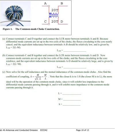
7 (c) Common-mode choke
For common-mode currents, the self inductance and mutual inductances of the choke reinforce each other so that more energy will be stored in the choke.
For differential-mode currents, the two inductances will cancel each other and therefore less energy will be stored in the choke.
Input Impedance with B-C short circuited
Leq(AD) = 2(L + M) C
20T
Input Impedance with B-D short circuited
(Core flux set up by each coil reinforces)
20T A
D Leq(AC) = 2(L - M)
D
A B
D
(Core flux set up by each coil cancels)
20T
20T
C
B
Common-mode choke construction and measurement: Wind 20 turns of two strands of wire around a toroidal
core (μR = 1250) to construct the common-mode choke shown above. Now determine L, M, and coefficient of
coupling k for this choke by performing the following measurements:
(a)Connect terminals C and D together and connect the LCR meter between terminals A and B. Because differential mode currents are set up in the two coils of the choke, the fluxes circulating in the core nearly cancel, and the equivalent inductance between terminals A-B should be relatively low, and is given by LAB = 2(L-M).
LAB = __________________
(b)Connect terminals C and B together and connect the LCR meter between terminals A and D. Now common-mode currents are set up in the two coils of the choke, and the fluxes circulating in the core reinforce, and the equivalent inductance between terminals A-D should be relatively large, and is given by LAD = 2(L+M).
LAD = __________________
(c)Now solve for the self inductance and the mutual inductance of the common-mode choke. Also find the coefficient of coupling,
L M L L M
k =
⋅
= . Note that the closer k is to 1.0 (the closer M is to L), the more
ideal will be the operation of the common-mode choke, since it will exhibit less impedance to the differential mode currents passing through it, and it will exhibit more impedance to the common-mode currents passing through it.
L = _______________
M = ______________
k = ______________
A
B
C
D
20T
[image:10.612.48.452.203.664.2]20T
7 (d) Switching Power Supply (DC-to-DC Inverter)
Here is a switching power supply that converts a 6 V DC input voltage to a 12 V DC output voltage if RL is very large (unloaded), or about 9 V when the output is loaded with RL = 50 ohms. The circuit uses two power Darlington transistors in a “blocking oscillator” configuration. The oscillation frequency is set by R1, R2, C1, and C2. These values have been adjusted so that the circuit oscillates at about 11 kHz. Due to the high relative permeability of the toroidal core that the center-tapped transformer is made from, the primary and secondary windings can be made with a relatively small number of turns, while still presenting an impedance at the switching frequency that is high enough to avoid severely loading down the oscillator circuit that drives the primary coil. During the first half of an oscillation cycle, transistor Q1 is saturated and Q2 is cut off, and thus the left-hand half of the 32-turn center-tapped primary winding conducts current to the left. During the second half of the oscillation cycle, Q2 is saturated and Q1 is cut off, so the right-hand half of the 32-turn primary winding conducts current to the right. Because the secondary winding has 32 turns, the voltage step-up ratio is roughly 32:16 = 2:1.
The 11 kHz switching frequency presents a problem from the EMC point of view. Common-mode RF currents couple onto the 2-wire 5 V power supply cable and are radiated, as indicated by a current probe that has been clamped around the dc input power cable (both wires) and connected to a spectrum analyzer. A common-mode choke (or ferrite bead, which is a 1-turn common-mode choke) can be used to help attenuate common-mode radiated, as well as conducted emissions associated with the dc power line..
D D1 RLOAD 50 ohm 20T Spectrum Analyzer Vb2 Vb1 20T
DC Power Cable
Current Probe Vc1 R2 15 K Q2 TIP102 32T Astable Push-Pull Blocking Oscillator fosc = 11.6 kHz Carries Differential-Mode Currents
Half-Wave Rectifier with Capacitor Filter & Common-Mode RF Noise Currents
Common-Mode Choke Vin Vout Vc2 C2 0.01 uF R1 15 K + DC-DC Inverter with Common-Mode
Choke inserted in DC Power Cable
-Toroidal CT Transformer
1N4004
6Vdc
16T
This common-mode choke will be inserted and then removed from circuit to observe its effect on common mode currents on the dc power cable as displayed on Spectrum Analyzer. 16T A C3 1000 uF B Q1 TIP102 C C1 0.01 uF
Vout(no load) = ________ Vout(50 Ω load) = __________ Vout (Bulb load) = _________
9. Emissions from Switching Mode DC-DC Inverter Circuit
b. Radiated emissions from switching power supply measured with short wire antenna attached to spectrum analyzer. (With and without common-mode choke installed) Describe observed results below:
c. Radiated Emissions after adding shield box over power supply circuit (shield not grounded.) With common-mode choke removed. Describe observed results below:
d. Radiated Emissions after adding shield box over power supply circuit (shield is connected to power supply ground.) With common-mode choke removed. Describe observed results below:
Now we desire to normalize (subtract out) this noise spectrum. Do this by making the following adjustments to the spectrum analyzer: View/Trace More Normalize Store Ref (1->3) Normalize Normalize Ref Position 5 Enter.
i. Now turn on DC Power Supply, but not the breadboarded switching power supply circuit under test, that is powered by the 5V output from this Agilent power supply. Observe and describe the resulting noise spectrum of the radiated emissions caused by the commercial dc power supply being turned on.
ii. Now energize breadboarded circuit (without common mode choke in dc power supply line), and observe and describe the increased radiated emission spectrum on the ac power line.