Abstract—A closed-loop scheme of high-gain serial-parallel switched-capacitor step-up converter (SPSCC) is proposed by combining a phase generator and pulse-width-modulation (PWM) controller for step-up DC-DC conversion and regulation. The SC-based converter needs no magnetic element, e.g. inductor and transformer. In this SPSCC, there are two 3-stage SC cells in cascade between source VS and output VO, where each cell has 3 pumping capacitors. By using these capacitors charging in parallel and discharging in series, plus the front-stage voltage connected in series, each SC cell can be treated as a small step-up converter with a 4× voltage gain.
Thus, this SPSCC is able to boost VO to 4×4 times voltage of VS
at most just with the fewer number of pumping capacitors (6 totally). Further, the PWM technique is adopted not only to enhance the output regulation for the compensation of the dynamic error between the practical and desired outputs, but also to reinforce output robustness against source or loading variation. Finally, the closed-loop SPSCC is designed by OrCAD SPICE, and simulated for some cases as: (1) steady-state response, (2) dynamic response (source/loading variation).
Index Terms—high-gain; serial-parallel; step-up; pulse- width-modulation; switched-capacitor (SC).
I. I
NTRODUCTIONecently, the demand for portable electronic devices has been increasing fast. With their light weight, small volume, multiple functionality and stand-alone power supply, these devices have found their way into many applications, such as PDA, E-book, cellular phone, etc. General speaking, this kind of portable equipments needs a small and compact power converter for converting battery voltage into the desired voltage value. However, the traditional converters have a larger volume and a heavier weight due to inductive elements, e.g. inductors and transformers. The SC-based power converter, possessing the power stage based on charge pump structure, is one of the good solutions to low-power DC-DC conversion because it has only semi- conductor switches and capacitors. Unlike traditional ones, inductor-less SC converters have light weight and small volume. Up to now, many SC types have been suggested and the well-known topologies are described as follows. In 1976, Dickson charge pump was proposed with two-phase clock connected with a diode chain via pumping capacitors [1].
But, its drawbacks included the fixed gain and larger device area. In 1997, Ioinovici and Zhu proposed SC circuit based on two symmetrical SC cells, and PWM was used for the output regulation enhancement [2-3]. In 2001, Starzyk presented a multiphase voltage double (MPVD) by multiphase operation. An n-stage Starzyk MPVD can boost voltage gain up to 2
nat most [4], i.e. the capacitor count in Starzyk is fewer for the same gain. Following the idea, Chang proposed many SC step-up/down DC-DC/DC-AC converters [5-7]. Nevertheless, some improved spaces still exist as follows:(i) Starzyk MPVD has the merits of fewer capacitor count and high gain, but it needs a complicated multiphase control circuit. Dickson charge pump or Ioinovici SC has a simple two-phase control circuit, but the gain is proportional to capacitor count. In this paper, the SPSCC scheme is presented for a compromise between capacitor count, voltage gain, and phase number of control circuit. Here, we use just 6 pumping capacitors to boost V
Oup to 4×4 times voltage of V
Sat most. (ii) Many SC circuits suffer from a limited regulation capability. For example, Starzyk MPVD circuit is fixed, the output voltage is also fixed. In this paper, we adopt PWM technique to com- pensate the error between the practical and desired outputs so as to enhance the output regulation as well as robustness against source/loading variation.
II. C
ONFIGURATION OFSPSCC
A. SPSCC schemeFig. 1 shows the overall circuit configuration of SPSCC, and it contians two major parts:“power part”and“control part ” for achieving the closed-loop step-up DC-DC conversion and regulation.
Firstly, the power part of SPSCC is shown in the upper half of Fig. 1, and it is mainly composed of two SC cells (cell A1 and cellA2) in cascade between source V
Sand output V
O. For more details, it includes 6 pumping capacitors (C
A11~C
A13, C
A21~C
A23), one output capacitor C
Land 8 switches (S1~S4, S5~S8*), where each capacitor has the same capacitance C (C
A11~C
A13=C
A21~C
A23=C). Fig. 2 shows the theoretical waveforms of 4 × 4 SPSCC in a switching cycle T
S. Each T
Scontains four small phases (Phase I, II, III and IV), and each phase has the same phase cycle T (T = T
S/4).
Secondly, the control part of SPSCC is shown in the lower half of Fig.1, and it is composed of low-pass filter (LPF), PWM block, and phase generator. From the view of controller signal flow, the feedback signal V
Ois sent into the OP-amp LPF for high-frequency noise rejection. Next the
R
Manuscript received December 2, 2011. This work is supported in part by the National Science Council of Taiwan, R.O.C., under Grant NSC 100-2221-E-324-005.
Yuen-Haw Chang and Song-Ying Kuo are with the Department and Graduate Institute of Computer Science and Information Engineering, Chaoyang University of Technology, Taichung, Taiwan, R.O.C. Post code:
413. (e-mail: cyhfyc@cyut.edu.tw, s9927637@cyut.edu.tw).
filtered signal V
Ois compared with the desired output reference Vref so as to produce the duty-cycle D via the PWM block. The main goal is to keep V
Oon following Vref by closed-loop duty-cycle adjustment. At the same time, the phase generator can be realized by digital logic gates to generate the switch driver signals (S1~S4, S5~S8*, S
A11~S
A16, and S
A21~S
A26). In addition, the PWM switch S8* is controlled by using logic-AND combination between S7 and duty-cycle D. In this paper, by using the PWM control, the regulation capability of SPSCC will be improved for different desired output.
B. Operation of SPSCC
In order to achieving step-up function, this converter needs two basic ways: charging into capacitors in parallel and discharging from capacitors in series. Next, we explain the detailed running steps of SPSCC for boosting the voltage gain of 4×4, 3×3, 2×2, respectively.
Operation of 4×4 SPSCC
(Please see the symbol “─────” of Fig. 3.) (i) Phase I:
S1, S2, S
A11~S
A14: turn on. Then, the Phase I topology is shown in Fig. 3(a). C
A11~C
A13(Cell A1) are charged in parallel by the V
S.
(ii) Phase II:
S3, S4, S5, S6, S
A15~S
A16, S
A21~S
A24: turn on. The Phase II topology is shown in Fig. 3(b). C
A11~C
A13(Cell A1) are discharged in series with the V
Sto transfer the power to C
A21~C
A23(Cell A2) in parallel.
(iii) Phase III:
It repeats Phase I operation as in Fig. 3(c). C
A11~C
A13(Cell A1) are charged in parallel by the V
S. (iv) Phase IV:
S3, S4, S7, S8* (PWM), S
A15~S
A16, S
A25~S
A26: turn on. The Phase IV topology is shown in Fig. 3(d).
C
A11~C
A13(Cell A1), C
A21~C
A23(Cell A2) are discharged in series with the V
Sto supply load R
Lvia PWM control of S8*.
Operation of 3×3 SPSCC
(Please see the symbol “─ ─ ─ ─” of Fig. 3.) (i) Phase I:
S1, S2, S
A11~S
A13: turn on. Then, the Phase I topology is shown in Fig. 3(a). C
A11~C
A12(Cells A1) are
charged in parallel by the V
S. (ii) Phase II:
S3, S4, S5, S6, S
A12, S
A15, S
A21~S
A23: turn on. The Phase II topology is shown in Fig. 3(b). C
A11~C
A12(Cell A1) are discharged in series with the V
Sto transfer the power to C
A21~C
A22(Cell A2) in parallel.
(iii) Phase III:
It repeats Phase I operation as in Fig. 3(c). C
A11~C
A12(Cell A1) are charged in parallel by the V
S. (iv) Phase IV:
S3, S4, S7, S8* (PWM), S
A12, S
A15, S
A22, S
A25: turn on. The Phase IV topology is shown in Fig. 3(d).
C
A11~C
A12(Cell A1), C
A21~C
A22(Cell A2) are discharged in series with the V
Sto supply load R
Lvia PWM control of S8*.
Fig. 1. Configuration of SPSCC.
Operation of 2×2 SPSCC
(Please see the symbol “─ • ─ • ─” of Fig. 3.) (i) Phase I:
S1, S2, S
A11: turn on. Then, the Phase I topology is shown in Fig. 3(a). C
A11(Cell A1) are charged in
parallel by the V
S. (ii) Phase II:
S3, S4, S5, S6, S
A11, S
A21: turn on. The Phase II topology is shown in Fig. 3(b). C
A11(Cell A1) are discharging in series with the V
Sto transfer the power to C
A21(Cell A2) in parallel.
(iii) Phase III:
It repeats Phase I operation as in Fig. 3(c). C
A11(Cell A1) are charged in parallel by theV
S.
(iv) Phase IV:
S3, S4, S7, S8* (PWM), S
A11, S
A21: turn on. The Phase IV topology is shown in Fig. 3(d). C
A11(Cell A1), C
A21(Cell A2) are discharged in series with the V
Sto supply load R
Lvia PWM control of S8*.
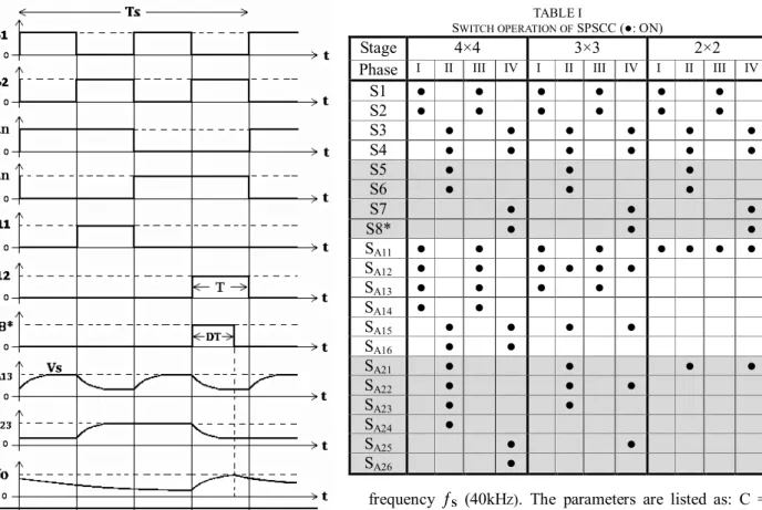
By changing the operation of the switches, the SPSCC has the different circuit topologies so as to obtain the various boosting gains (e.g. 4×4, 3×3, 2×2). The switch operation for the various gains is shown in Table I, where S8* is a PWM-ON switch.
III. S
IMULATION OFSPSCC
In this section, based on Fig. 1, the closed-loop SPSCC converter is designed and simulated by OrCAD SPICE tool.
The results are illustrated to verify the efficacy of the proposed scheme. The main function of SPSCC is to convert V
O to 4×4, 3×3, 2×2 times voltage of VSat most (V
S= 3V) for supplying load R
L(300Ω) at switching
frequency ƒ
S(40kH
Z). The parameters are listed as: C = 400μF, C
L= 550μF (ESR 8mΩ), and the on-state resistance of switches is assumed at 0.005mΩ. Some cases will be simulated and discussed, including: (i) steady-state response, (ii) dynamic response (source/loading variation).
(i) Steady-state response:
The closed-loop 4×4/3×3/2×2 SPSCC is simulated for Verf = 47.5V/27.0V/12.0V respectively, and then these output results are obtained as shown in Fig. 4(a)-(b)/Fig. 4 (c)-(d)/Fig. 4(e)-(f). In Fig. 4(a), it is found that the settling time is about 20ms, and the steady-state value of V
Ois really reaching 47.18V, and converter is stable to keep V
Ofollowing Vref (47.5V). In Fig. 4(b), the output ripple percentage is measured as rp = Δvo/V
O= 0.0317%, and the power efficiency is obtained as η = 99.4%. In Fig. 4(c), it is found that the settling time is smaller than 15ms, and the steady-state value of V
Ois really reaching 26.74V, and converter is stable to keep V
Ofollowing Vref (27.0V). In Fig. 4(d), the output ripple percentage is measured as rp = Δvo/V
O= 0.0281%, and the power efficiency is obtained as
η = 99.6%. InFig. 4(e), it is found that the settling time is smaller than 10ms, and the steady-state value of V
Ois really reaching 11.934V, and converter is stable to keep V
Ofollowing Vref (12.0V). In Fig. 4(f), the output ripple percentage can be easily found as rp = Δvo/V
O=0.0335%, and the power efficiency is obtained as η = 99.3%.
Obviously, these results show that the step-up converter has a pretty good steady-state performance.
(ii) Dynamic response:
Since the source voltage is decreasing naturally with the running time of battery, or varying due to the bad quality battery, the output robustness against source noises must be considered. In the first case, it is assumed that source voltage starts at DC 3.0V, and then have a voltage drop at 20ms form 3.0V→2.5V as in the upper half of Fig. 5(a).
Fig. 2. Theoretical waveforms of 4×4 SPSCC.
S8* ● ● ●
S
A11● ● ● ● ● ● ● ●
S
A12● ● ● ● ● ●
S
A13● ● ● ●
S
A14● ●
S
A15● ● ● ●
S
A16● ●
S
A21● ● ● ●
S
A22● ● ●
S
A23● ●
S
A24●
S
A25● ●
S
A26●
From the lower half of Fig. 5(a), obviously, V
Ois still keeping on 39V (Vref=39V), even though V
Shas the disturbance lower than standard source of 3.0V. In the second case, assume that V
Sis the DC value of 3.0V and extra plus a sinusoidal disturbance of 0.3V as in the
upper half of Fig. 5(b), and the waveform of V
Ois shown in the lower half. Cleary, V
Ois still keeping Vref (47.5V) in spite of sinusoidal disturbance. In the third case, the regulation capability for loading variation is discussed.
Assume R is 300Ω normally, and it changes from 300Ω to
(a) Phase I.
(b) Phase II.
(c) Phase III.
(d) Phase IV.
Fig. 3. Topologies of SPSCC. (4×4: ────, 3×3: ─ ─ ─, 2×2: ─ • ─ • ─)
60Ω at 20ms. After a short period, the load recovers from 60Ω to 300Ω at 40ms, i.e. R
L= 300Ω→60Ω→300Ω. Fig.
5(c) shows the transient waveform of V
Oat the moment of loading variations. It is found that V
Ohas a small drop at 20ms~40ms and the curve shape becomes thicker during the heavier load, i.e. the output ripple becomes bigger at this moment. These results show that the closed-loop SPSCC has the good output robustness to source/loading variations.
IV. C
ONCLUSIONSA closed-loop scheme of high-gain SPSCC is proposed by combining a phase generator and PWM controller for step-up DC-DC conversion and regulation. The advantages of the proposed scheme are listed as follows. (i) The SC-based SPSCC needs no magnetic element, so I.C.
fabrication will be promising. (ii) This SPSCC use just 6 pumping capacitors to boost V
Oup to 4×4 times voltage of V
Sat most. (iii) By changing the operation of the switches,
the SPSCC has the different circuit topologies so as to obtain the various boosting gains (e.g. 4×4, 3×3, 2×2). (iv) Since using COMS gate as a bidirectional switch, it is helpful to integrate various the step-up topologies into one structure. (v) By using PWM technique, the output regulation is enhanced as well as robustness to source/
loading variation. At present, we have implemented the hardware of SPSCC as shown the photo in Fig. 6. Next, some more experimental results will be obtained and measured for the verification of our SPSCC.
0V
0s 10ms 20ms 30ms 40ms 50ms
47.24V
47.22V
47.20V
47.18V
47.16V
47.14V
47.12V
49.70ms 49.75ms 49.80ms 49.85ms 49.90ms 49.95ms 50ms
Fig. 4. SPSCC steady-state response.
(a) VO = 47.18V. (4×4 SPSCC)
(b) rp = 0.0317%. (4×4 SPSCC)
14V
12V
10V
8V
6V
4V
2V
0V
0s 10ms 20ms 30ms 40ms 50ms
49.70ms 49.75ms 49.80ms 49.85ms 49.90ms 49.95ms 50ms
11.950V
11.945V
11.940V
11.935V
11.930V
11.925V
11.920V 28V
24V
20V
16V 12V
8V
4V
0V
0s 10ms 20ms 30ms 40ms 50ms
49.50ms 49.60ms 49.70ms 49.80ms 49.90ms 50ms 26.71V
(c) VO = 26.74V. (3×3 SPSCC)
(e) VO= 11.934V. (2×2 SPSCC) (d) rp = 0.0281%. (3×3 SPSCC)
(f) rp= 0.0335%. (2×2 SPSCC)
R
EFERENCES[1] J. K. Dickson, “On-chip high-voltage generation in MNOS integrated circuits using an improved voltage multiplier technique,” IEEE J. Solid-State Circuit, vol. SC:-11, pp. 374–378, Fed. 1976.
[2] S. V. Cheong, S. H. Chung, and A. Ioinovici, “Duty-cycle control boosts dc-dc converters,” IEEE Circuits and Devices Mag., vol. 9, no.2, pp.36-37, 1993.
[3] Guangyong Zhu, Adrian Ioinovici, “DC-to-DC converter with no magnetic elements and enhanced regulation,” IEEE Transactions on Aerospace and Electronic Systems vol. 33, no. 2, pp.499-505, Apple 1997.
[4] Starzyk, J.A., Ying-Wei Jan, Fengjing Qiu, “A DC-DC charge pump design based on voltage doublers,” IEEE Transactions on Circuits and Systems-I: Fundamental Theory and Applications, vol.
[5] Y.-H. Chang, “Design and analysis of pulse-width-modulation- based two-stage current-mode multi-phase voltage doubler,” IET Circuits Devices Systems, vol. 4, issue 4, pp. 269-281, July, 2010.
[6] Y.-H. Chang, “Design and analysis of multistage multiphase switched-capacitor boost DC-AC inverter,” IEEE Trans. Circuits and Systems-I: Regular paper, vol. 58, no. 1, pp. 205-218, January, 2011.
[7] Y.-H. Chang, “Variable-conversion-ratio multistage switched- capacitor-voltage-multiplier/divider DC-DC converter,” IEEE Transactions on Circuit and Systems-I: Regular Papers, vol. 58, no.
8, pp. 1944-1957, August 2011.
3.3V 3.2V
3.0V
2.8V 2.7V
0s 10ms 20ms 30ms 40ms 50ms
60V
40V
20V
0V
0s 10ms 20ms 30ms 40ms 50ms 60V
40V
20V
0V
0s 10ms 20ms 30ms 40ms 50ms 40V
30V
20V 10V
0V
Fig. 5. SPSCC dynamic response.
(a) Source voltage VS=3V→2.5V.
Output voltage VO=39V.
(b)Source voltage VS=3±0.3sinwt.
Output voltage VO=47.18V.
(c) Waveform of VO when RL=300Ω→60Ω→300Ω.
5.0V 4.0V 3.0V 2.0V 1.0V 0V 3.0V
2.8V
2.6V 2.5V
Fig. 6. Hardware implementation of SPSCC.
←────────300Ω──────→←───────60Ω───────→←─300Ω─→