International Journal of Emerging Technology and Advanced Engineering
Website: www.ijetae.com (ISSN 2250-2459, ISO 9001:2008 Certified Journal, Volume 7, Issue 6, June 2017)
283
Design and Simulation of High Electron Mobility Transistor
using Silvaco TCAD
Kamal Prakash pandey
1, Anil Kumar
2, A.K. Jaiswal
31Research scholar, 2Assistant Professor, 3Professor, Department of ECE, SHUATS, Allahabad, UP- India.
Abstract:We have design and simulate GaN High electron mobility transistors (HEMTs) for high voltage and high speed applications. Simple AlGaN/GaNon sapphire substrates HEMT and HEMT with oxide layer was proposed for achieving high current carrying capability as well as high speed switching capability and analyzed using ATLAS (SILVACO) simulator. The device characteristics suggest that the MOS-HEMT has better performance compared to the conventional HEMT. Advantages of HEMT on the basis of band gap, electron mobility, saturation drift velocity and power handling capacity has also been discussed. Simulation result shows the effect of temperature on the cutoff frequency, for temperature 248k the technology 90nm has the cutoff frequency of 24.1GHz while for the same technology at higher temperature of 373k the cutoff frequency decrease to 9 GHz.
Keywords: HEMT, Gallium Nitride (GaN), MOSHEMT, Silvaco TCAD, Heterojunctions.
I. INTRODUCTION
In the past few years, Gallium Nitride (GaN) has been a matter of attraction over Silicon (Si) due to several advantages such as large band gap energy, high critical electric field, high electron mobility, high saturation drift velocity and melting point. [1]Few applications of GaN includes light emitting diode for display technology, LASERS, Microwave amplifiers, radiation hardness devices, power devices, switching devices etc. [2]Due to high mobility, GaN on Si technology is emerging as one of the best alternate to the well-developed Si technology for switching devices[3, 4].
In conversion of power, transistors basically work as an ideal switch. For the power devices the main requirement is high breakdown voltage and low energy loss. [5] The energy loss can be classified into two forms static and dynamic, static losses occur when the transistor is in the on-state and off-state. [6]
Ideally in the on-state a transistor should have a very low on-resistance in order to decrease the power losses and in the off-state the transistor should behave as a perfect open circuit offering infinite current but, inevitably, results in some residual current, or leakage current flows. This leakage current should be very small in order to reduce the static power dissipation to zero. Another is the dynamic power dissipation in which the loss is due to the parasitic capacitance and inductance. Gate turn-off thyristor (GTO) and insulated gate bipolar transistor that works between Hz and kHz while GaN and Si-MOSFET devices have a frequency response of MHz. The GaN technology resulted in not only extends the operational frequency but also, in the switching capacity of the MOSFET devices. [7]
As the power devices require high breakdown voltage for the high voltage operation, lower resistance for low loss and low capacitance for low dynamic power dissipation. [8] These properties can’t be fulfilled by the silicon and germanium in terms of breakdown voltage and speed of device. So we need those materials which have higher energy band gap than these electronic dominating materials. Such materials are popularly known as the Wide Band Gap Semiconductors. Example of such materials is Silicon Carbide, Gallium Nitride and its various related heterostructures. These wide gap materials have very high band gap that results in high breakdown voltage and thus help to increase the RF power [9-10]. In this paper we have investigated the properties of semiconductor materials for the power devices and various problems associated with the devices. Further, the physics of heterostructures and heterojunctions is explained and simulated.
II. HEMTSTRUCTURE
International Journal of Emerging Technology and Advanced Engineering
Website: www.ijetae.com (ISSN 2250-2459, ISO 9001:2008 Certified Journal, Volume 7, Issue 6, June 2017)
284
Table 1.1:Bandgap, dielectric Constant, thermal conductivity and critical electric field. [11]
Materials Material Properties Ban
d Gap (Eg)
Diele ctric Const ant
Thermal Conductivit y
(K(W/m3))
Breakdo wn Field (*105 V/cm)
Si 1.12 11.9 1.5 3.0
GaAs 1.43 12.5 0.54 3.0
InP 1.34 12.4 0.67 4.5
3C-SiC 2.3 9.7 4.0 1.8
4H-SiC 3.2 10.0 4.0 3.5
6H-SiC 2.86 10.0 4.0 3.8
GaN 3.4 9.5 1.3 2.0
Diamond 5.6 5.5 20-30 2.0
As per the energy band gap, heterostructures are classified as the type I, type II, and type III. In type I heterostructures the total sum of the conduction band and valence band edge discontinuities is equal to the energy gap difference. Example of such heterostructure is GaAs-AlGaAs, GaN-AlGaN, and their band diagram shown in figure 1.
Figure1. Energy Band diagrams of various heterostructures. All the values are in eV.
The basic structure of AlGaN/GaN HEMT with nucleation layer, buffer and the channel layers, the finally the barrier layer and as well as a capis shown in figure 2.
Figure2. AlGaN/GaN HEMT basic structure showing all layers. [12]
[image:2.612.327.557.181.350.2]International Journal of Emerging Technology and Advanced Engineering
Website: www.ijetae.com (ISSN 2250-2459, ISO 9001:2008 Certified Journal, Volume 7, Issue 6, June 2017)
285
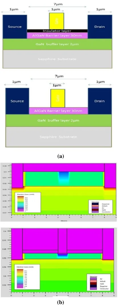
Figure3. MOSHEMT and conventional HEMT with and without insulating layer (a) Model structure, (b) Structure on Silvaco. The
gate length is kept to be 1µm and the channel length is 7µm.
III. RESULTS AND DISCUSSION
[image:3.612.67.274.136.668.2]Figure 4 shows the Output (Drain Current Vs Drain Voltage) characteristic of the MOS and conventional HEMT, the gate length of the device is 1000nm with drain to source spacing of 7µm.
Figure 4: ID vs. VDS MOS -HEMT and Conventional HEMT at 1µm
gate length. RED lines represent the drain current for the MOS HEMT and BLACK lines for the Conventional HEMT.
Initially the current is approximately zero for the very low drain voltage. But as the drain voltage increases the drain current also increases linearly and finally gets saturated after much higher drain voltage. Thus the linear region of the characteristic is up to VDS=5V for VGS=3V.Beyond the VDS=5V the drain current starts saturating. The electrical characteristics shows higher drain current and lower gate leakage in the MOS HEMT as compared to the conventional HEMT, which is due higher degree of 2DEG at the interface of AlGaN/GaN. The transfer characteristics of the two devices are shown in figure 5.
Figure5. ID VS VGS of MOSHEMT and HEMT of1000nm gate length.
RED lines represent the drain current for the MOS HEMT and BLACK lines for the Conventional HEMT.
(a)
[image:3.612.328.576.528.694.2]International Journal of Emerging Technology and Advanced Engineering
Website: www.ijetae.com (ISSN 2250-2459, ISO 9001:2008 Certified Journal, Volume 7, Issue 6, June 2017)
286
The turn ON voltage of the MOSHEMT is found to be -7V as compared to the conventional HEMT having TURN ON voltage of -3V, making it less prone to noise. The
[image:4.612.330.556.135.450.2]energy band diagram of the two devices is shown in figure 6.
Figure 6: Energy Band Diagram of MOS HEMT and Conventional HEMT with 1000nm gate length and channel length 7µm using
3nmAl2O3 as insulation layer. For VGS=3V and VDS=20V.
The band gap in the channel i.e. GaN of MOSHEMT is found to be approximately 3.5eV while in the GaN of HEMT it nearly 3.2eV.The electric field and electron density in the channel of the two devices are shown in figure 7.
Figure 7: (a) Electric Field and (b) electron Concentration comparison of at the channel for the Conventional HEMT and MOS HEMT using Al2O3 as oxide layer. Channel length=7µm, gate length
=1µm, For VGS=3V and VDS=20V.
(a)
[image:4.612.53.283.198.429.2]International Journal of Emerging Technology and Advanced Engineering
Website: www.ijetae.com (ISSN 2250-2459, ISO 9001:2008 Certified Journal, Volume 7, Issue 6, June 2017)
287
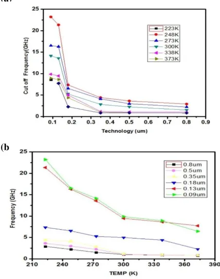
Result shows that the electron in the Conventional HEMT suffers from the large amount of scattering. The electric field at the interface of the MOSHEMT is approximately 570KV/cm while at the interface of the Conventional HEMT it is found to be 490KV/cm. On comparing the electron density, we get electron concentration is higher in the MOSHEMTand is found to be nearly~10E20 which is quite greater than the conventional HEMT. The cutoff frequency of the MOSHEMT with various channel length is shown in figure 8.
Figure 8 (a) (b): Cutoff Frequency Variation with various Technologies with the effect of temperature.
Reducing the technology parameter increases the cutoff frequency. Another advantage of decreasing the channel length is that the current carrying capability increases as the current flowing in the device is always indirectly proportional to the channel length. For a particular temperature, the frequency response decreases as the technology increases. As visible in the graph for temperature 248k the technology 90nm has the cutoff frequency of 24.1GHz while for the same technology at higher temperature of 373k the cutoff frequency decrease to 9GHz.
The main reason of decrease of the frequency response at the higher temperature is due to scattering.
IV. CONCLUSION
MOSHEMT and Conventional HEMT structures were simulated on the Silvaco TCAD. Results shows that the MOS-HEMT has better performance than the conventional HEMT. Moreover, it can replace the well-established technology of silicon in the field of power devices due to its large bandgap, high electron mobility and high saturation drift velocity of the 3rd -5th group materials compared to the 4th group materials. Effect of channel length and temperature on the cutoff frequency has also been investigated.
REFERENCES
[1] Shealy, J., Smart, J., Poulton, M., Sadler, R., Grider, D., Gibb, S., & Garber, P. (2002, October). Gallium nitride (GaN) HEMT's: progress and potential for commercial applications. In Gallium Arsenide Integrated Circuit (GaAs IC) Symposium, 2002. 24th Annual Technical Digest (pp. 243-246). IEEE.
[2] Pearton, Stephen, ed. GaN and ZnO-based materials and devices.
Vol. 156. Springer Science & Business Media, 2012.
[3] Baliga, B. Jayant. "Power semiconductor device figure of merit for high-frequency applications." IEEE Electron Device Letters 10.10 (1989): 455-457.
[4] Hower, Philip L., Sameer Pendharkar, and Taylor Efland. "Current status and future trends in silicon power devices." Electron Devices Meeting (IEDM), 2010 IEEE International. IEEE, 2010.
[5] Lorenz, L., et al. "COOLMOS/sup TM/-a new milestone in high
voltage power MOS." Power Semiconductor Devices and ICs, 1999. ISPSD'99. Proceedings. The 11th International Symposium on. IEEE, 1999.
[6] Letor, Romeo. "Static and dynamic behavior of paralleled
IGBTs." IEEE transactions on industry applications 28.2 (1992): 395-402.
[7] Lidow, Alex, et al. GaN transistors for efficient power conversion. John Wiley & Sons, 2014.
[8] Mishra, Umesh K., et al. "GaN-based RF power devices and
amplifiers." Proceedings of the IEEE 96.2 (2008): 287-305.
[9] Chow, T. Paul, and RituTyagi. "Wide bandgap compound
semiconductors for superior high-voltage power devices." Power Semiconductor Devices and ICs, 1993. ISPSD'93., Proceedings of the 5th International Symposium on. IEEE, 1993.
[10] Neudeck, Philip G., Robert S. Okojie, and Liang-Yu Chen.
"High-temperature electronics-a role for wide bandgap
semiconductors?" Proceedings of the IEEE 90.6 (2002): 1065-1076.
[11] Bhatnagar, Mohit, and B. Jayant Baliga. "Comparison of 6H-SiC, 3C-SiC, and Si for power devices." IEEE Transactions on Electron Devices 40.3 (1993): 645-655.
[12] Schwierz, F., Liou, Juin J., Modern Microwave Transistors: Theory, Design, and Performance: Theory, Design and Performance. John Wiley & Sons, 2002.
(a)
[image:5.612.50.276.274.560.2] [image:5.612.323.565.326.691.2]