International Journal of Emerging Technology and Advanced Engineering
Website: www.ijetae.com (ISSN 2250-2459,ISO 9001:2008 Certified Journal, Volume 4, Issue 2, February 2014)
926
Power Reduction for Sequential Circuit using Merge
Flip-Flop Technique
S.Tamil Selvi
1, P.Sukumar
21
PG Scholar (VLSI Design), Nandha Engineering College
2Assistant Professor (Electronics and Communication Engineering), Nandha Engineering college
Abstract— Flip-Flops are the major storage element and most power consumption component in a sequential circuit. In integrated circuits the power consumed by clocking is more than 50% of the system power because of its transition probability. Given a design we can reduce its power consumption by replacing several flip-flops with some multi-bit flip-flop. This may affect the performance of the original circuit because of its timing and placement capacity constraints. To overcome this problem efficiently, a technique combination table is introduced to enumerate possible combinations of flip-flops provided by a library. Finally we use a hierarchical way to merge flip-flops. Besides power reduction, the objective of minimizing the total wirelength is also considered. In this paper, the multi-bit flip-flop is introduced in ip-dco technique to reduce power consumption
Keywords— clock power reduction,combination table, ip-dco,multi-bit flip-flop, merging
I.
INTRODUCTION
A clock system and a logic part consume dominant part of the total chip power. The clock system itself consumes 20-45% of the chip power. In this clock system power, 90% is consumed by the flip-flops themselves and the last branches of the clock distribution network which directly drives the flip-flops .This is due to the high switching activity
.
Pclk= Cclkv2ddfclk (1)
Where Pclk is clock power, fclk is the clock frequency,Vdd is
the supply voltage, and Cclk is the switching capacitance
including the gate capacitance of flip-flops(Sequential Element)controlled by the clock signal, the interconnect capacitance of the clock network, and the capacitance associated with the buffers/inverters used in the clock network.
Several methodologies [2], [3] have been proposed to reduce the power consumption of clocking. Given a design that the locations of the cells have been determined, the power consumed by clocking can be reduced further by replacing several flip-flops with the multi-bit flip-flops.
In clock tree synthesis if less number of flip-flop means less number of clock sink. Thus, the resulting clock network would have less power consumption and less routing resource By applying MBFFs the advantages are: 1) smaller design area due to shared clock drivers and less routing resource 2) Less delay and less power of clock network due to fewer clock sinks 3) Controllable clock skew because of common clock and enable signals for the group of flip-flops and reduced depth of a clock tree
International Journal of Emerging Technology and Advanced Engineering
Website: www.ijetae.com (ISSN 2250-2459,ISO 9001:2008 Certified Journal, Volume 4, Issue 2, February 2014)
927 However, the locations of some flip-flops would be changed after this replacement, and thus the wirelength of nets connecting pins to a flip-flop are also changed. To avoid violating the timing constraints, we restrict that the wirelengths of nets connecting pins to a flip-flop cannot be longer than specified values after this process.
Besides, to guarantee that a new flip-flop can be placed within the desired region, we also need to consider the area capacity of the region. To avoid the timing violation caused by the replacement, the Manhattan distance of new nets net1,
net2, net3, and net4 cannot be longer than the specified
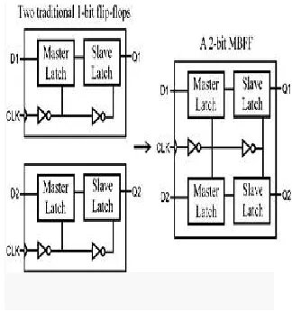
[image:2.612.94.256.352.525.2]values. The replacement of some flip-flops with multi-bit flip- flops would change the routing length of the nets that connect to a flip-flop, it inevitably changes timing of some paths
Fig .1.Replacing two traditional FFs by a 2-bit FF
II.
RELATED WORK
Chang et al. [6] first proposed the problem of using multi-bit flip-flops to reduce power consumption in the post-placement stage. They use the graph-based approach to deal with this problem. In a graph, each node represents a flip-flop. If two flip-flops can be replaced by a new flip-flop without violating timing and capacity constraints, they build an edge between the corresponding nodes. After the graph is built, the problem of replacement of flip-flops can be solved by finding an m-clique in the graph. The flip-flops corresponding to the nodes in an m-clique can be replaced by an m-bit flip-flop.
They use the branch-and-bound and backtracking algorithm [8] to find all m-cliques in a graph. Because one node (flip-flop) may belong to several m-cliques (m-bit flip-flop), they use greedy heuristic algorithm to find the maximum independent set of cliques, which every node only belongs to one clique, while finding m cliques groups. However, if some nodes correspond to k-bit flip-flops that k ≥1, the bit width summation of flip-flops corresponding to nodes in an m-clique, j , may not equal m. if the type of a j-bit flip-flop is not supported by the library, it may be time-wasting in finding impossible combinations of flip-flops.
III.
OUR ALGORITHM
Our design flow can be roughly divided into three stages. Please see Fig. 2 for our flow. In the beginning, we have to identify a legal placement regionfor each flip-flop f1. First, the feasible placement regions of a flip-flop associated with different pins are found based on the timing constraints defined on the pins. Then, the legal placement region of the flip-flop fi can be obtained by the overlapped area of these
[image:2.612.398.521.456.652.2]regions. However, because these regions are in the diamond shape, it is not easy to identify the overlapped area.
International Journal of Emerging Technology and Advanced Engineering
Website: www.ijetae.com (ISSN 2250-2459,ISO 9001:2008 Certified Journal, Volume 4, Issue 2, February 2014)
[image:3.612.344.572.186.487.2]928 In the second stage, we would like to build a combinationtable, which defines all possible combinations of flip-flops in order to get a new multi-bit flip-flop provided by the library.The flip-flops can be merged with the help of the table. After the legal placement regions of flip-flops are found and the combination table is built, we can use them to merge flip- flops. To speed up our program, we will divide a chip into several bins and merge flip-flops in a local bin. However, the flip-flops in different bins may be mergeable. Thus, we have to combine several bins into a larger bin and repeat this step until no flip-flop can be merged anymore.
A. Build a Combination Table
If we want to replace several flip-flops by a new flip-flop fi’, we have to make sure that the new flip-flop fi’ is provided
by the library L when the feasible regions of these flip-flops overlap. Now a combination table is to be built, which records all possible combinations of flip-flops to get feasible flip-flops before replacements. Initialize the combination table T with the flip-flop provided by the library.For simplicity use binary tree to represent the several combination of flip-flops.Each node in the tree denotes one type of flip-flop in L.Pseudo type flip-flops are added to the library inorder to enumerate all possible combinations.For example,assume that a library only supports two kinds of flip-flops whose bit widths are 1 and 4 respectively.In order to use a combination whose bit width is 4, there must exist flip-flops whose bit widths are 2 and 3in L. The bit width of flip-flop added should be larger than the minimum width available and smaller than the maximum width of flip-flop in the library.
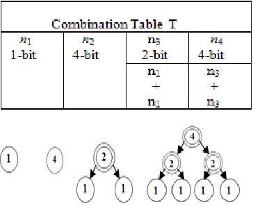
Fig.3 (a) Initialize the library L and the combination table T. (b) Pseudo types are added intoL, and the corresponding binary tree is also build for each combination in T
Thus we can gradually replace flip-flops according to the combinations of flip-flop in this table Fig.3 shows the Example of building the combination table;
(c)
(d)
Fig.3(c) new combination n3 is obtained from combining two n1s
[image:3.612.57.250.565.661.2]International Journal of Emerging Technology and Advanced Engineering
Website: www.ijetae.com (ISSN 2250-2459,ISO 9001:2008 Certified Journal, Volume 4, Issue 2, February 2014)
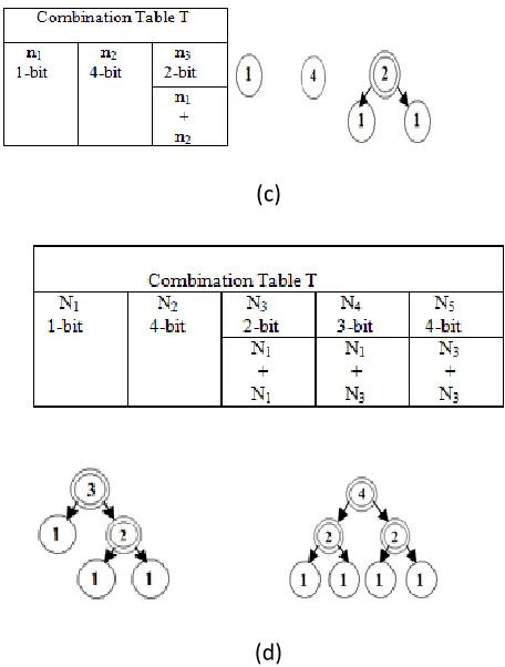
929 (e)
Fig 3(e) new combination n6 is obtained from combining n1 and n4
Next the function of insert pseudo type is performed to check whether the flip-flop types with bit widths between 1 and 4 exist or not. Thus, two kinds of flop types of flip-flops in L are sorted according to their bit widths. Finally, n6 is obtained by combining n1 and n4.all possible combinations of flip-flops are shown in fig. 3(e). Among combinations, n5 and n6 are duplicated since they both represent the same condition, which replaces four 1-bit flip-flops by a 4-bit flip-flop.
Fig 3(f) last combination table is obtained after deleting the unused combination in fig 3(e)
B. Merge Flip-Flops
After the combination table is built the combination of flip-flops are used for merging and replacing. To reduce the complexity the whole placement region is divided into several sub regions. Then, several subregions are combined into a larger subregion and the flip-flops are replaced again so that those flip-flops in the neighboring subregions can be replaced further. Finally, those flip- flops with pseudo types are deleted in the last stage because they are not provided by the supported library.
a) Region Partition: To speed up our problem, we divide
[image:4.612.54.262.147.235.2]the whole chip into several subregions. By suitable partition, the computation complexity of merging flip-flops can be reduced significantly. As shown in Fig.7, we divide the region into several subregions, and each subregion contains six bins, where a bin is the smallest unit of a subregion.
Fig. 4 Example of region partition with six bins in one sub region
b) Replacement of Flip-flops in Each Subregion: Before
illustrating the procedure to merge flip-flops, first an equation is given to measure the quality if two flip- flops are going to be replaced by a new flip-flop as follows:
Cost=routing_length−α×√ (available_area) (2)
Where routing_length denotes the total routing length between the new flip-flop and the pins connected to it, and available_ area represents the available area in the feasible region for placing the new flip-flop. α is a weighting factor. After a combination has been built, we will do the replacement of flip-flops according to the combination table. First, the flip-flops are linked below with the corresponding types available in the library. From leaves to root the right and left child of flip-flops are merged serially. Then, combination cost is computed for each pair of flip-flop in the respective list so the pair with the smallest cost is chosen. Finally, we add a flip-flop f’ in the list of the combination n and remove the picked flip-flops which constitutes the f’.
[image:4.612.350.526.228.310.2] [image:4.612.52.234.372.524.2]International Journal of Emerging Technology and Advanced Engineering
Website: www.ijetae.com (ISSN 2250-2459,ISO 9001:2008 Certified Journal, Volume 4, Issue 2, February 2014)
930 Each pair of flip-flops in n1 are selected and checked to see if they can be combined The pair with the smallest cost value is chosen to break the tie. In Fig. 5(a), f1 and f2 are chosen because their combination gains the smallest cost. Thus, we add a new node f3 in the list below n4, and then delete f1 and f2 from their original list [see Fig. 5(b)].Similarly f4 and f5 are combined to obtain a new flip-flop
f6, and the result is shown in fig 5(c). After all combination in
1-level tree are obtained the procedure then moves to 2-level trees. Similarly n6 and n7 combination are obtained by merging
flip-flops shown in fig 5(d) and 5(e).When there exists no pair of flip-flop that can be combined further, the procedure finishes as shown in fig. 5(f)
(a) (b)
Fig. 5(a) sets of flip-flops before merging Fig. 5(b) Two 1-bit flip-flops, f1 and f2, are replaced by the2-bit flip-flop
Fig.5(c). After all flip-flops in the combinations of 1-level trees (n4 and n5) are obtained as shown in Fig. 5(d), we start to form the flip-flop in the combinations of 2-level trees (n6 and n7)
(
e) (f)Fig.5 (e) Two 2-bit flip-flops, f3 and f6, are replaced by the 4-bit flip-flop
f10. Fig.5 (f) Sets of flip-flops after merging.
If the available overlap region of two flip-flops exists, we can assign a new one to replace those flip-flops. Once there is sufficient space to place the new flip-flop in the available region, the algorithm will perform the replacement,, and the new generated flip-flop will be placed in the grid that makes the wirelength between the flip-flop and its connected pins smallest. If the capacity constraint of the bin, Bk, which
the grid belongs to will be violated after the new flip-flop, is placed on that grid, we will search the bins near Bk to find a
new available grid for the new flip-flop
IV.
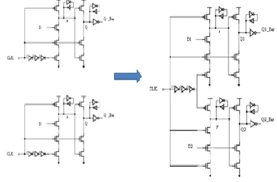
IP-DCO FLIP-FLOPPulse-triggered FF (P-FF) has been considered a popular alternative to the conventional master–slave based FF in the applications of high-speed operations. Ip-dco is known as the implicit data close to output. It is an implicit type flip-flop. In this method the pulse is generated inside the flip-flop. The concept of multi-bit flip-flop has been introduced in ip-dco technique where it can reduce the dynamic power consumption by merging and by sharing the same clock
[image:5.612.48.240.310.405.2]buffer
.
Fig 6. Replacing two traditional ip-dco FFs by a 2-bit ip-dco FF
[image:5.612.350.549.445.576.2] [image:5.612.50.245.448.524.2] [image:5.612.49.243.570.687.2]International Journal of Emerging Technology and Advanced Engineering
Website: www.ijetae.com (ISSN 2250-2459,ISO 9001:2008 Certified Journal, Volume 4, Issue 2, February 2014)
931 The pulse generator takes complementary and delay skewed clock signals to generate a transparent window equal in size to the delay by inverters I1-I3. First, during the rising edge, nMOS transistors N2 and N3 are turned on. If data remains high, node X will be discharged on every rising edge of the clock.
V.
RESULT AND DISCUSSIONS
In this algorithm, there exist two values which would affect our results: the first one is the dimension of a subregion since we would partition a chip into several subregions. The second one is the parameter used in the cost function of (2). Thus, we first do some experiments to explore better values for these two parameters
1) Influence of Region Size on Performance: In this part, we
first determine a s uitable size for each subregion during partitioning. Since the execution time is actually dominated by the average number of flip-flops included in a subregion, we use the number of flip-flops in a single subregion to represent the size of a subregion, which can be obtained from multiplying the number of bins in a subregion by the average number of flip-flop about 83% and 0.8% if the number of flip-flops in a single subregion is 600
2) Influence of Weighting Factor α on Performance: Since
the parameter α used by (6) would affect our results, it is necessary to find a suitable value for getting better results. In this experiment, we sweep α from 0 to 3 to get the data of power consumption and wirelength. While the value of α becomes larger, the power reduction ratio gets larger.
VI.
SIMULATION RESULT
Multi-bit flip-flop methodology can be synthesized by XILINX Design Compiler. Experimental results indicate that multi-bit flip-flop is very effective and efficient method in lower-power designs
.
TABLE I
COMPARISON RESULTSOF POWER
Parameter Existing flip-flop
Merged flip-flop
Power 39mw 32mw
Fig 7.Simulation result
VII. CONCLUSION
This paper has proposed an algorithm for flip-flop replacement for power reduction in digital integrated circuit design. The procedure of flip-flop replacements is depending on the combination table, which records the relationships among the flip-flop types. The concept of pseudo type is introduced to help to enumerate all possible combinations in the combination table. By the guidelines of replacements from the combination table, the impossible combinations
International Journal of Emerging Technology and Advanced Engineering
Website: www.ijetae.com (ISSN 2250-2459,ISO 9001:2008 Certified Journal, Volume 4, Issue 2, February 2014)
932
REFERENCE
[1] L-T Wang, Y-W chang, and K.-T cheng Eds., “Electronic design automation: synthesis, verification and Test”.
Burlington,MA:Elsevier/Morgan,Kaufmann 2009
[2] Duarte D, Narayanan V and Irwin M. J (Apr. 2002) “Impact of technology scaling in the clock power,” in Proc. IEEE VLSI
Comput. Soc. Annu. Symp, Pittsburgh, PA, pp. 52–57.
[3] Gronowski P, Bowhill W. J,Preston R. P, Gowan M. K, andAllmon R. L, (May 1998 )“High-performance microprocessor design,” IEEE J. Solid-State Circuits, Vol.33.,
No.5., pp. 676–686.
[4] Bron C and Kerbosch J,(1973) “Algorithm 457: Finding all cliques of a Undirected graph,” ACM Commun., Vol.16.,
No.9., pp. 575–577.
[5] Cheon Y, Ho P.H, Kahng A.B,Reda S, and Wang Q(Jun. 2005) “Power-Aware placement,” in Proc. Design Autom. Conf., pp. 795–800. K. Elissa, “Title of paper if known,” unpublished.
[6] Chang Y.-T, Hsu C.-C, Lin P.-H,.Tsai Y.-W, and Chen S.-F(Nov. 2010) “Post-placement power optimization with multi-bit flip-flops,” in Proc.IEEE/ACM Comput.-Aided Design Int. Conf., San Jose, CA,pp. 218–223.
[7] The Hamada M C. K,, Fujita T, Hara H, Ikumi N, and Oowaki Y(Dec. 2006) “Conditional data mapping flip-flops for low-power and high-performance systems,” IEEE Trans. Very Large
Scale Integration. (VLSI) Systems, Vol.14, pp. 1379–1383,.
[8] Kawagachi H. and Sakurai T( Jun.1997)“A reduced clock-swing flip-flop (RCSFF) for 63% clock power reduction,” in