International Journal of Emerging Technology and Advanced Engineering
Website: www.ijetae.com (ISSN 2250-2459, ISO 9001:2008 Certified Journal, Volume 6, Issue 9, September 2016)
83
A Review on Detection of PCB Defects based on Image
Processing Techniques & Proposal of an Approach to Improve
the Detection Level
Er. Amit Paul
1, Er. Gaurav
2, Er. Poonam Verma
31M-Tech Student, 2,3Assistant Professor, Electronics & Communication, Shaheed Udham Singh College of Engineering and
Technology, Tangori, Punjab, India
Abstract— In the present scenario, the PCB industry is growing at very high scale as the low cost and reliability offered by the PCB industries make it more enthusiastic for automation and household purposes. In this paper, we make a comparative study for various techniques based on image processing developed till date to determine the defects on PCB’s and proposed a method based on LBP (Local Binary Pattern) There is a two level hierarchy where inspection for defects is mainly required for qualitative as well as quantitative manufacturing process. Starting from finding abnormal designing, defect detection like wrong holes, defects while etching, broken lines etc., the system will decide whether the PCB is accepted or rejected. On 2nd level hierarchy, defects based on placement of various components are detected using the template image of the PCB’s. We also study various modifications that can be widely used for texture classifications using different combinations. Our main focus is to find defects on PCB’s.
Keywords— PCB defects, Defect Classification, Texture Classification, Local Binary Pattern, image subtraction, template matching.
I. INTRODUCTION
Printed circuit board (PCB) is one of the key tools in the electronics and automation industries. To ensure the high quality and reliable digital products based on PCB’s, we have to inspect the quality of printed circuit board from the very initial step of designing. Before the introduction of fully digital techniques, manual inspection systems were widely used for inspecting the conditions of the bare PCB’s. Manual inspection systems were based on visual analysis which was carried out by human operators. Sometimes defects in PCB’s are not visible by naked eyes and required microscopic level of inspection which involves the collaboration of both manual and digital techniques. By the time, introduction of image processing gives a revolutionary turn in finding defects.
In comparison to visual inspection by human operators, the digital processing methods are both cost efficient and less prone to error as digital processing involves the comparison with the reference image of the true PCB with the testing image.
II. TYPE OF PCBDEFECTS TO BE DETECTED
When we are taking into consideration that the PCB should be of zero-defect than we have to look for both offline and online detection which categorizes the defects into two types i.e. functional defects and cosmetic defects[1] When the defects are detected during the online inspection means whether the signal processing through different routes is considered as the functional defects. Rest all types of defects occurred during the manufacturing process or during components placing time is considered as cosmetic defects.
As the error probability during online working is directly dependent on the quality of PCB at manufacturing level, we have to focus on the various cosmetic defects and how to reduce the error at its initial stage [5]. There are 14 main cosmetic defects widely found on PCB as shown in figure and named as follows:-
i. Breakout ii. Pin hole iii. Open circuit iv. Under-Etch
v. Mouse-bite vi. Missing conductor vii. Sput
viii. Short
International Journal of Emerging Technology and Advanced Engineering
Website: www.ijetae.com (ISSN 2250-2459, ISO 9001:2008 Certified Journal, Volume 6, Issue 9, September 2016)
[image:2.612.57.279.128.355.2]84
Fig.1 Different types of cosmetic defects in PCB [4]
III. LITERATURE SURVEY
This section is covering the background aspects for both PCB defect detection and different methodologies used till date.
Mohit Borthakur [1] et al. makes a comparative study of different algorithms developed and propose an approach based on hybrid approach combining both morphological image segmentation and other simple operations like noise removal, wavelet transformation and subtraction method.
F.Moganti [ 2] et al. proposed a broad classification of PCB inspection into three levels. These all three are based on automation and classified as referential approach, non- referential approach and hybrid approach. Furthermore these three approaches are further classified as shown in table given below:-
Table1.
Classification of different Inspection Approach [2]
Heriansyah [3] et al. proposed an approach that classifies the defects occurred on PCB using Neural network. The approach segments the image into primitive patterns, patterns normalization and classification were developed using morphological image processing and linear vector quantization neural network.
Khalid [4] et al. proposed an algorithm that can be implemented on bare PCB to identify and to group PCB defects. Major drawback of this algorithm is that it is developed to work with binary images only, whereas the output from the cameras is in gray scale format. Although the conversion can be made from gray scale to binary format imperfection still can be occurred.
Indera Putera [5] et al provides improvement to Khalid’s work by classifying seven groups. This is done by combining image processing algorithm and the segmentation algorithm.
Fabiana R. Leta [6] et al proposed an algorithm which involves comparing a PCB standard with a PCB image, using a simple subtraction algorithm. The main difficulty arises in the pre-processing technique.
S.H Indera Putera [7] et al. proposed a non-contact reference based image processing approach for defect detection and classification. But, in this approach there are many limitations which are as follows: Unwanted images were also generated by noise during gray-scale to binary conversion; Pin-hole defect was ignored.
IV. PROBLEM FORMULATION
The basic automated PCB defect detection starts with morphological operations performed on PCBs are erosion, dilation, opening, closing, boundary extraction etc. This basic process of defect detection using morphological operations can be implemented only to detect the defects in tracks of PCBs. So on a basic level it is successful, but once mounted PCBs are used and defects are to be detected, then it fails.
The next best approach that has been used so far is the image subtraction operation using XOR operator .This process compares pixel by pixel value of the standard image to a test image in order to detect the defects. This algorithm runs fast and gives better results only when defects in tracks are to be detected as it has only two levels of pixel values to compare, one for the tracks and the other for background. The same process takes a lot of time to produce results once we consider a mounted PCB. It happens because there is increase in pixel values to be compared with and even though it gives a true output but the execution time is still very long.
S. No. Approach Further Classification
1 Referential approach i. Model based inspection
ii. Image comparison
2 Non-Referential
approach
i. Morphological processing
ii. Encoding techniques
International Journal of Emerging Technology and Advanced Engineering
Website: www.ijetae.com (ISSN 2250-2459, ISO 9001:2008 Certified Journal, Volume 6, Issue 9, September 2016)
85 It takes approximately 2.20 minutes to give the results of operation after simulation, which is quite a long time when we consider industry parameters. It is very much required to focus on the performance of the system in terms of processing time. The cost of system depends on the size and composition of the input image. When we consider the tracks only, the size of the image is small. But as soon as we consider a mounted PCB, sizes may vary in the range of 600x400 pixels and even more. Haar wavelet transform has been proposed as an extension to the previous system to reduce the size of the image. Once the size of the image gets reduced, image subtraction operation can be performed again to the same image after compression. But this algorithm too has its shortcomings like Wavelet transform compresses the image and because of it, certain small but important information part of an image gets neglected. This may lead to discrepancies in the output image as features missed in compression may result in defects after subtraction, which in reality may not be an actual defect.
V. INTRODUCTION TO LOCAL BINARY PATTERNS
The basic local binary pattern operator, firstly introduce by Ojala et al. [8], based on the hypothesis that texture has locally two complementary aspects, a pattern and its strength. The LBP was proposed to describe the local textural patterns as a two-level task. The inventive version of the technique operator works in a 3 × 3 pixel block of an image. The first step involves the operator working with the eight-neighbors of a pixel, using the center pixel value as a threshold. An LBP code for the local area was produced by multiplying the threshold values with binary weights given to the corresponding pixels, and adding up the result. As the neighborhood consists of 8 pixels, a total of 256 different labels can be obtained depending on the comparative gray values of the center and the pixels in the local neighborhood. In its simplest form the LBP operator takes the pixel and generates a binary 1 if the value of neighbor of the centre pixel has larger value than the centre pixel.
Fig.2 Example for calculation of Local Binary Pattern code
The operator generates a binary 0 if the neighbor is less than the centre. The eight neighbors of the centre can then be represented with an bit number such as an unsigned 8-bit integer, making it a very compact description. Fig.2 shows an example of an LBP operator. As sampling of neighborhood during LBP codes is done using circular path, which makes calculations invariant to the rotation of the image. When an image is founded rotated, it refers that
the gray level values
g
p move along the perimeter of theselected circular neighborhood at
g
c Since theneighborhood is always indexed counter-clockwise, starting in the direction of the positive x axis, the rotation of the image naturally results in a different
LBP
P R, value. However it is not applied to all zeros (black) or all ones (white) which remains constant at all rotation angles. To remove the effect of rotation, each LBP code must be rotated back to a reference position, effectively making all rotated versions of a binary code the same. This transformation can be defined as follows:, min{ ( , , ) 0,1... 1 }
ri
P R P R
LBP ROR LBP i i P
Fig.3 Effect of rotation invariant LBP on image rotation
VI. OBJECTIVE
The main focus of this paper is to become the familiar with defects types that are occurred on PCB and the various methods which are widely used for detection of defects. This paper also includes various techniques based on Local Binary Pattern and an approach based on LBP for texture classification for defining the different types of defects. The objective of the proposed project includes:
To design a real time application for defect detection in PCB at different level of manufacturing.
To enhance the local feature extraction and localize the defect using LBP.
International Journal of Emerging Technology and Advanced Engineering
Website: www.ijetae.com (ISSN 2250-2459, ISO 9001:2008 Certified Journal, Volume 6, Issue 9, September 2016)
86 Time comparison graphs are drawn on the basis of time
consumed by proposed work in comparison with present state of art techniques.
VII. BLOCK DIAGRAM OF THE PROPOSED WORK
[image:4.612.325.563.231.369.2]To overcome the shortcomings of all previous algorithms, a better and faster process is proposed which provides quantitative as well as qualitative results.
Fig. 4 Block diagram for the proposed work
The proposed system follows the following steps:-
The first step is to read the sample image of the non-defective PCB and the sample image of the PCB to be tested.
Selection of symmetric neighborhood set for both the images.
Convert the RGB image into HSV domain.
Calculate and store the threshold values for each neighborhood set covering the whole image using Local binary pattern technique.
Compare both template and test images of PCBs using Local Binary Pattern to find out the defects.
VIII. RESULTS
The results generated focused on thoroughly testing the realization of the PCB’s defects and its localization on the basis of Local Binary Patterns.
The results showed that the algorithm can accurately detect and locate the defects corresponding to a template scanned image of PCB.
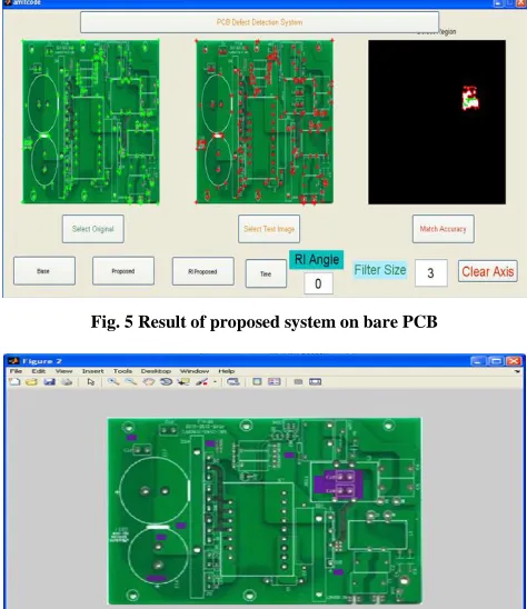
[image:4.612.325.562.235.509.2]The results further confirmed starts from a user friendly GUI (Graphical User Interface) which is providing a Select Original button to pick a template image and Select Test button pick a Test image and preview for the both images on the same GUI.
Fig. 5 Result of proposed system on bare PCB
[image:4.612.84.238.241.476.2]Fig. 6 Defected region obtained by proposed system
[image:4.612.325.562.552.695.2]International Journal of Emerging Technology and Advanced Engineering
Website: www.ijetae.com (ISSN 2250-2459, ISO 9001:2008 Certified Journal, Volume 6, Issue 9, September 2016)
[image:5.612.54.573.82.721.2]87
[image:5.612.319.565.119.271.2]Fig. 8 Comparison graphs for vertical projection
Fig. 9 Result of proposed system on component placed PCB
[image:5.612.46.292.130.271.2]Fig. 10 Defected region obtained by proposed system
[image:5.612.319.566.283.707.2]Fig. 11 Comparison graphs for horizontal projection
Fig. 12 Comparison graphs for vertical projection
[image:5.612.47.287.295.433.2] [image:5.612.47.286.456.593.2]International Journal of Emerging Technology and Advanced Engineering
Website: www.ijetae.com (ISSN 2250-2459, ISO 9001:2008 Certified Journal, Volume 6, Issue 9, September 2016)
88
Fig.14 Time comparison for component placed PCB’s samples.
IX. CONCLUSION
The work is successfully implemented on both types of PCB’s either bare or components placed by comparing images of PCB to detect and to locate the defects on PCB. By comparing, the research work with the existing work, it is observed that this presented work is giving better result than the existing works, because this work produces the output without degrading or compressing of the quality of the image. Furthermore it is also applied to color images of PCB’s as well as on gray scale images. Due to its fast processing in computations, proposed algorithm can be applied as real time application with conveyor belts as an online testing algorithm.One direction for future expansion of the software will be building it with more specific criterion regarding selection of filter size as in accordance with input test image size as it is easier and having quick response with a fixed filter size for particular size of test image which is manually selected under the proposed system.
REFERENCES
[1] Mohit Borthakur, Anagha Latne, Pooja Kulkarni 2015, ―A
Comparative Study of Automated PCB Defect Detection Algorithms and to Propose an Optimal Approach to Improve the Technique‖, International Journal of Computer Applications (0975 – 8887) Volume 114 – No. 6, pp. 27-33.
[2] Moganti, F. Ercal, C. H. Dagli, S.Tsunekawa 1996, ―Automatic PCB
inspection algorithms: A survey, Computer Vision and Image Understanding‖, Vol. 63,No. 2, pp. 287-313.
[3] A. S.H Indera Putera, Z.Ibrahim , 2012, ―Printed Circuit Board Defect Detection Using Mathematical Morphology and MAT LAB Image Processing Tools,‖ Universiti Teknologi MARA, 40450 Shah Alam, Selangor Malaysia, vol. 5, pp. 359–363.
[4] K. Khalid, Z. Ibrahim, M. S.Z. Abidin 2008, ―An algorithm to group defects on printedcircuit board for automated visual inspection‖, IJSSST, Vol. 9, No. 2, pp. 1-10.
[5] Indera Putera and Z.Ibrahim, ― Printed Circuit Board Defect Detection Using Mathematical Morphology and MAT LAB Image Processing Tools‖ IEEE 2nd International Conference on Education Technology and Computer (ICETC).
[6] Indera Putera and Z.Ibrahim 2010, ― Printed Circuit Board Defect Detection Using Mathematical Morphology and MAT LAB Image Processing Tools‖ IEEE 2nd International Conference on Education Technology and Computer (ICETC).
[7] Fabiana R. Leta, Flavio F. Feliciano, Flavius P.R. Martins 2008, ―Computer Vision System For Printed Circuit Board Inspection‖, ABCM Symposium Series in Mechatronics, Vol. 3, pp.623-632. [8] Timo Ojala, Pietikainen and Topi Maenpaa 2002, ―Multiresolution
Gray-Scale and Rotation Invariant Texture Classification with Local Binary Patterns‖, IEEE Transactions On Pattern Analysis And Machine Intelligence, Vol. 24, NO. 7, pp. 971-987.
[9] Amit Satpathy, Xudong Jiang and How-Lung Eng 2014,
―LBP-Based Edge-Texture Features for Object Recognition‖, IEEE Transactions On Image Processing, Vol. 23, No. 5, pp. 1953-1964. [10] Timo Ahonen, Abdenour Hadid, and Matti Pietikainen 2006, ―Face
Description with Local Binary Patterns: Application to Face Recognition‖, IEEE Transactions on Pattern Analysis and Machine Intelligence, Vol. 28, No. 12, pp.2037–2041.
[11] Di Huang, Caifeng Shan, Mohsen Ardebilian, Yunhong Wang, and Liming Chen 2011, ―Local Binary Patterns and Its Application to Facial Image Analysis: A Survey‖, IEEE Transactions on Volume 41, No. 6, pp. 765 – 781.
[12] Prachi P. Londe, S.A. Chavan 2014, ―Automatic PCB Defects Detection and Classification using Matlab‖, International Journal of Current Engineering and Technology, Vol.4, No.3.
[13] Swagata Ray, Joydeep Mukherjee 2015, ― A Hybrid Approach for Detection and Classification of the Defects on Printed Circuit Board‖, International Journal of Computer Applications (0975 – 8887) Volume 121 – No.12, pp. 42-48.
[14] Ajay Pal Singh Chauhan, Sharat Chandra Bhardwaj 2011,
―Detection of Bare PCB Defects by Image Subtraction Method using Machine Vision‖, Proceedings of the World Congress on Engineering, Vol II, WCE 2011, July 6 – 8, pp. 1597-1601. [15] http://www.scholarpedia.org/article/Local_Binary_Patterns
![Fig.1 Different types of cosmetic defects in PCB [4]](https://thumb-us.123doks.com/thumbv2/123dok_us/8689820.876870/2.612.57.279.128.355/fig-different-types-cosmetic-defects-pcb.webp)