sensors
ISSN 1424-8220www.mdpi.com/journal/sensors
Review
Gas Sensors Based on One Dimensional Nanostructured
Metal-Oxides: A Review
M. M. Arafat 1, B. Dinan 2, Sheikh A. Akbar 2 and A. S. M. A. Haseeb 1,*
1
Department of Mechanical Engineering, Faculty of Engineering, University of Malaya, 50603 Kuala Lumpur, Malaysia; E-Mail: arafat_mahmood@siswa.um.edu.my
2
Department of Materials Science and Engineering, The Ohio State University, 2041 College Road, Columbus, OH 43210, USA; E-Mails: dinan@matsceng.ohio-state.edu (B.D.);
akbar.1@osu.edu (S.A.A.)
* Author to whom correspondence should be addressed; E-Mail: haseeb@um.edu.my; Tel.: +603-7967-4598; Fax: +603-7967-4448.
Received: 2 April 2012; in revised form: 18 April 2012 / Accepted: 11 May 2012 / Published: 30 May 2012
Abstract: Recently one dimensional (1-D) nanostructured metal-oxides have attracted much attention because of their potential applications in gas sensors. 1-D nanostructured metal-oxides provide high surface to volume ratio, while maintaining good chemical and thermal stabilities with minimal power consumption and low weight. In recent years, various processing routes have been developed for the synthesis of 1-D nanostructured metal-oxides such as hydrothermal, ultrasonic irradiation, electrospinning, anodization, sol-gel, molten-salt, carbothermal reduction, solid-state chemical reaction, thermal evaporation, vapor-phase transport, aerosol, RF sputtering, molecular beam epitaxy, chemical vapor deposition, gas-phase assisted nanocarving, UV lithography and dry plasma etching. A variety of sensor fabrication processing routes have also been developed. Depending on the materials, morphology and fabrication process the performance of the sensor towards a specific gas shows a varying degree of success. This article reviews and evaluates the performance of 1-D nanostructured metal-oxide gas sensors based on ZnO, SnO2, TiO2, In2O3, WOx, AgVO3, CdO, MoO3, CuO, TeO2 and Fe2O3. Advantages and disadvantages of each sensor are summarized, along with the associated sensing mechanism. Finally, the article concludes with some future directions of research.
1. Introduction
Semiconducting metal-oxides are promising candidates for gas sensing applications because of their high sensitivity towards many target gases in conjunction with easy fabrication methods, low cost and high compatibility with other parts and processes [1–4]. To date, ZnO, SnO2, TiO2, In2O3, WO3, TeO2, CuO, CdO, Fe2O3 and MoO3 nanostructures have been developed with different dimensions and sensor configurations. It was found that both the surface state and morphology of the metal-oxides play important roles in gas sensing performance [5]. Depending on the application of interest and availability of fabrication methods, different surface morphology and configurations of the metal-oxides have been achieved; including single crystals, thin films, thick films and one dimensional (1-D) nanostructures [6]. Of these, 1-D nanostructures have attracted much attention in recent years because of their potential applications in gas sensors [7]. 1-D nanostructures are particularly suited to this application because of their high surface-to-volume ratio as well as their good chemical and thermal stabilities under different operating conditions [8,9].
Development of fabrication methods for producing 1-D nanostructures has been a major focus in the field of nanoscience and nanotechnology [10]. Several routes have been investigated for 1-D metal-oxide nanostructures for gas sensing applications. These include hydrothermal [11], ultrasonic irradiation [12], electrospinning [13], anodization [14], sol-gel [15], molten-salt [16], carbothermal reduction [17], solid-state chemical reaction [18], thermal evaporation [19], vapor-phase transport [20], aerosol [21], RF sputtering [22], molecular beam epitaxy [23], chemical vapor deposition [24], nanocarving [25], UV lithography and dry plasma etching [26]. Depending on the processing route and treatments, different types of nanostructures with different surface morphology can be achieved. Some examples of nanostructures produced by these methods include nanorods [5,7], nanotubes [14], nanowires [17], nanofibers [13], nanobelts [22], nanoribbons [27], nanowhiskers [28], nanoneedles [29], nanopushpins [30], fibre-mats [21], urchins [31], and lamellar [32] and hierarchical dendrites [20]. However, these variations in morphology showed a varying degree of success at detecting different types of reducing and oxidizing gases such as H2, H2S, NH3, CO, NO2, O2, liquefied petroleum gas (LPG), ethanol, methanol, xylene, propane, toluene, acetone and triethylamine.
The sensor’s response to a given gas can be enhanced by the modification of both surface states and bulk properties of the 1-D metal-oxide nanostructures. These modifications can be achieved by either depositing nanoparticles on the nanostructure’s surface, or coating and doping with impurities. Sensors utilizing these types of surface and bulk property modifications showed somewhat higher sensitivity compared to unmodified systems.
2. Gas Sensor Performance Characteristics
Semiconducting materials generally owe their conductivity to their deviation from stoichiometry [33]. Interstitial cation and anion vacancies also play an important role in the conductivity [33]. In general, semiconductor metal-oxide sensors operate by virtue of gas adsorption on the surface that leads to a change in the electrical resistance of the oxide. Based on the charge carrier, semiconducting materials can be divided into two groups: n-type (electrons are major carrier, such as ZnO, SnO2, TiO2, In2O3, WOx, AgVO3, CdO and MoO3) and p-type (holes are major carrier, such as CuO, NiO and TeO2) materials. Target gas species can also be classified into two groups: oxidizing gas or electron acceptors such as O2, NO2 and reducing gas or electron donor such as H2, H2S, HCHO, CO and ethanol. When a reducing gas is chemisorbed on the surface of an n-type material, extra electrons are provided to the material surface. As a result the resistivity of n-type material is decreased. The opposite is observed for p-type materials. This type of electrical modification is utilized for gas sensing.
In the literature, sensitivity, response time, recovery time, optimum working temperature and lower limit of detection are reported as the main performance parameters of a sensor. Throughout the literature, sensor sensitivity (S) is defined in several different forms including S = Ra/Rg, S = Rg/Ra,
S = ∆R/Rg and S = ∆R/Ra; where Ra is the sensor resistance in ambient air, Rg is the sensor resistance in the target gas, and ∆R = |Ra−Rg| [7,34,35]. In this literature review, the sensitivity values are reported as presented by the author. The formula used to calculate the sensitivity is also indicated. Response time is defined as the time required for a sensor to reach 90% of the total response of the signal such as resistance upon exposure to the target gas. Recovery time is defined as the time required for a sensor to return to 90% of the original baseline signal upon removal the target gas.
3. Fabrication of Gas Sensor with 1-D Nanostructures
1-D nanostructures used in the fabrication of gas sensors include metal-oxides in the form of nanorods, nanowires, nanofibers, nanotubes, nanobelts, nanoribbons, nanowhiskers, nanoneedles, nanopushpins, fibre-mats, urchin, lamellar and hierarchical dendrites. Nanorods, nanowire, nanofibers and nanotubes are rod shaped nanostructures having a diameter ranging from 1–200 nm. The aspect ratios (length divided by width) of nanorods and nanowires are 2–20 and greater than 20, respectively [36]. However, nanofibers have higher aspect ratio than nanowires. Nanotubes are basically hollow nanorods with a defined wall thickness. The definition of other nanostructures, such as nanobelts [22,37,38], nanoribbons [27], nanowhiskers [28], nanoneedles [29,39], nanopushpins [30], fibre-mats [21], urchin [31], lamellar [32] and hierarchical dendrites [20] can be found in the respective literatures. It is important to mention that the distinction between the different nanostructures is not always self evident and the terms are often used interchangeably from one reference to another.
These nanostructures can be arranged in different ways for the fabrication of a sensor. Figure 1 illustrates the predominant types of nanostructure arrangements and electrode attachment methods reported in literature. The nanostructure arrangements can be divided into three groups: (a) single nanostructure arrangement, (b) aligned arrangement and (c) random arrangement.
ratio [11,40]. Lupan et al. [11] developed an in-situ lift-out technique for arranging a single ZnO nanorod on a glass substrate to be used in H2 sensing applications. One single ZnO nanorod was attached to an electro-polished tungsten wire and positioned on a glass substrate containing a square hole for gas entrance. The nanorod was connected to the external electrodes as shown in Figure 2. Similarly, by using an in-situ lift-out technique by focused ion beam (FIB), single tripod and tetrapod gas sensors were developed from single ZnO nanorods by Lupan et al. [41,42] and Chai et al. [43]. Their technique obtained a 90% success rate for building prototypes of nano/micro-sensors based on individual nanoarchitectures from metal oxides.
Figure 1. Schematics of sensor fabrication containing (a) a single nanostructure. (b) aligned nanostructures and (c) randomly distributed nanostructures.
Figure 2. Scanning electron microscopy (SEM) images showing the steps of the in-situ
[image:4.595.56.520.270.440.2] [image:4.595.116.481.562.777.2]For aligned nanostructure arrangements (Figure 1(b)), the nanostructure arrays are normally grown on a thin film. For example, Varghese et al. [44] developed a sensor device containing a TiO2 nanotube array which was adopted for exploring gas sensing properties. In this sensor, TiO2 nanotubes were grown from Ti foil by anodization [44]. A barrier layer also formed between the Ti foil and nanotubes during the process. Two spring-loaded parallel Pt pads (100 µm thickness) were used to contact the nanotubes electrically. A similar type of gas sensor was developed by Liao et al. [45] for detecting ethanol where ZnO nanorod arrays were sandwiched between a silicon substrate and an indium thin film. The indium thin film provided the Ohmic contact and a copper sheet was used as an electrode.
Randomly distributed nanostructured sensors can have three variations: (i) nanostructures randomly distributed in the form of a film, (ii) randomly distributed nanostructures deposited on the circumference of a tube and (iii) randomly distributed nanostructures pressed into a tablet form. Wan et al. [9] used a flat interdigitated substrate where randomly distributed ZnO nanowires were dispersed in ethanol by ultrasonication directly coated onto a silicon-based interdigitated substrate by spin coating (Figures 1(c) and 3). This is common practice where the as-grown nanostructures are directly coated on the substrate through a standard technique such as spin coating [9]. Sometimes nanowire growth and attachment with the substrate is integrated with the device formation [46,47].
[image:5.595.143.452.407.503.2]Figure 3. (a) Top view of the Pt interdigitated silicon substrate. (b) Schematic of the fabricated sensor structure [9].
Figure 4. Schematic illustration of a tube-type 1-D nanostructured gas sensor [31].
[image:5.595.202.395.545.673.2]tube-type ceramic sensor for the detection of H2S. Porous 1-D α-Fe2O3 nano-urchins were mixed with terpineol to form a paste which was then coated uniformly onto the outside surface of an alumina tube having a diameter of 1 mm and length of 5 mm. A Ni-Cr alloy resistance heating coil was placed inside the tube to maintain the operating temperature. Pt wires were attached to gold electrodes for making the electrical contacts and finally connected to outside electronics for monitoring the resistance change. To improve performance, the gas sensors were heat treated at 300 °C for 10 days in air.
[image:6.595.50.547.298.601.2]Randomly distributed nanostructures can also be used to fabricate tablet-type sensors. Zhou et al. [48] used such type of a sensor for ethanol gas. ZnO nanorods were formed in the shape of pellets under a 6 MPa pressure. The dimension of the pellets was 3 mm in thickness with a 5.3 cm2 area. High purity silver paste was used as an electrode and attached at the front and back side of the ZnO pellets by spin coating.
Table 1. Fabrication parameters of tube-type gas sensors reported in literature.
Sensor Materials Sensor Material Morphology Materials for Paste Formation Ceramic Tube Material
Ceramic Tube Dimension
Electrodes Heating
Material
Operating
Temperature
Range (°C)
Reference Length
(mm)
External
Diameter
(mm)
Internal
Diameter
(mm)
ZnO Nanorod
Poly(vinyl
acetate)
(PVA)
Al2O3 8 2 1.6 Au Ni–Cr 100–500 [5]
ZnO Nanorod Terpineol Al2O3 – – – - - – [18]
SnO2 Nanorod
Poly(vinyl
acetate)
(PVA)
Al2O3 8 2 1.6 Au Ni-Cr 100–500 [49]
SnO2 Nanofiber
Deionized
water – – – – Au Ni-Cr – [13]
TiO2
(Cu-doped) Nanofiber
Deionized
water – – – – Au Ni-Cr – [50]
In2O3 Nanorod
Deionized
water Al2O3 4 1.4 1 Au – – [15]
In2O3 Nanowire
Poly(vinyl
acetate)
(PVA)
Al2O3 8 2 1.6 Au Ni-Cr 100–500 [51]
α-Fe2O3 Porous urchin Terpineol Al2O3 5 1 - Pt Ni–Cr 100–500 [31]
4. 1-D Nanostructured Materials for Gas Sensing
4.1. 1-D ZnO Nanostructured Gas Sensors
4.1.1. Growth and Characterization of ZnO Nanostructures
[image:7.595.47.547.301.774.2]The processing routes developed for the growth of 1-D ZnO nanostructures can be divided into three categories: (i) wet processing routes, (ii) solid-state processing routes and (iii) vapor-phase processing routes. Wet processing routes include hydrothermal and ultrasonic irradiation in an aqueous solution, while carbothermal reduction and solid-state chemical reaction are examples of solid-state processing routes for the production of ZnO nanostructure. Vapor-phase processing routes include molecular beam epitaxy (MBE), RF sputtering, aerosol, thermal evaporation, vapor-phase transport and chemical vapor deposition. Processing details for the growth of 1-D ZnO nanostructure are summarized in Table 2.
Table 2. Summary of various processing routes for the production of 1-D ZnO nanostructures. Processing Route Synthesis Method Starting Materials Synthesis Temperature
(°C)
Morphology Diameter of ZnO nanostructure Length of ZnO nanostructure Reference Wet Processing route Hydrothermal
ZnAc2, NaOH, absolute ethanol,
distilled water 180 Nanorod – – [5]
Zn(CH3COO)2·2H2O,
C6H8O7·H2O, absolute ethanol,
distilled water
400
Nanorod (vertically
aligned)
50 nm 500 nm [7]
Zn(NO3)2·6H2O, NaOH,
cetyltrimethyl ammonium bromide, ethanol
120 Nanorod – – [48]
Zn(NO3)2·6H2O, NaOH,
cyclohexylamine, ethanol, water 200 Nanorod 150–200 nm 2 µm [52] Zn(SO4)·7H2O, NH4OH,
deionized water 75–95 Nanorod – – [11]
NaOH, Zn(NO3)2, absolute
ethanol, deionized water, hydroethylenediamine
180 Flowerlike 150 nm Few micrometer [53]
Ultrasonic irradation in aqueous solution
Deposited Zn layer on interdigitated alumina substrate, Zn(NO3)2·6H2O, (CH2)6N4
–
Nanorod (vertically aligned)
50 nm 500 nm [12]
Solid-state processing route
Carbothermal Reduction
ZnO powder, graphite powder, Ar gas flow, Au coated silicon substrate
900–925 Nanowire 80–120 nm 10–20 µm [17,54]
Solid-state chemical reaction
ZnCl2, NaOH, polyethylene
glycol, Na2WO4·2H2O
RT Nanorod 40–60 nm 200 nm [18]
20–40 nm 100 nm
Vapor-phase processing route
Thermal evaporation
Zn metal, O2, Ar 650–670 Nanowire 100 nm Several microns [55]
Zn metal pellets, O2, Ar 900 Nanowire 20 nm – [19]
Zn powder, O2, Ar 600 Nanowire 80 nm 1 µm [56]
Vapor-phase transport
ZnO powder, graphite,
Cu catalist 930
Hierarchical
dendrite 60–800 nm – [20]
Aerosol Zn powder, N2 gas 500–750
Fiber-mat 100–300 nm –
[21] Cauliflower 20–30 nm –
RF sputtering ZnO deposited over Pt sputtered
interdigitated alumina substrate − Nanobelt – Few micrometer [22] Molecular beam
epitaxy
Zn metal, O3/O2 plasma
Figure 5. ZnO nanostructures. (a) Randomly distributed nanorods produced by hydrothermal process [48]. (b) Flowerlike nanorods produced by hydrothermal process [53]. (c) Vertically aligned nanorods produced by chemical vapor deposition process [55]. (d) Hierarchical dendrites produced by vapor-phase transport process [20].
Hydrothermal processing is the most widely employed method for the production of 1-D ZnO nanostructures due to its simplicity, low growth temperature, short growth interval, and ease of transfer of the product to other substrates [11]. Although the starting materials in a hydrothermal process vary widely, in all cases the main goal is to produce Zn(OH)42− ions which acts as a precursor for the fabrication of 1-D ZnO nanostructure (Table 2). The nanostructures obtained by hydrothermal process are mostly nanorods with different configurations such as vertically aligned [7], randomly distributed (Figure 5(a) and flowerlike (Figure 5(b)). It is seen that the addition of water in the hydrothermal process has a significant effect on the resulting nanostructure [52]. Addition of no or very low water content causes agglomeration and urchin type morphology of ZnO nanostructure. For obtaining ZnO nanorods, the addition of water is substantial. Recently, another simple wet processing route has been developed for the fabrication of vertically aligned ZnO nanorods by ultrasonic irradiation [12]. In this process, a Zn thin film was deposited on an interdigitated alumina substrate by RF sputtering technique. An ultrasonic wave was introduced to the sample after immersing the substrate in an aqueous solution containing Zn(NO3)2·6H2O and (CH2)6N4.
[image:8.595.148.448.159.425.2]NaOH with a molar ratio of 1:2 in presence of polyethylene glycol. The reaction involved the release of heat and evaporation of water vapor. It was suggested that in this process Zn(OH)2 precursor was formed by reacting ZnCl2 and NaOH, which subsequently decomposed into ZnO nanorods by an exothermic reaction. By adding Na2WO4-2H2O to the solution smaller nanorods were produced.
Vapor-phase processing has also been widely used for producing ZnO nanostructures. For example, Lupan et al. [55] grew vertically aligned ZnO nanowire (Figure 5(c)) by chemical vapor deposition (CVD) from Zn metal and O2/Ar flux. The Zn metal was evaporated at 670 °C in a quartz tube. The evaporated metal interacted with O2 at 650 °C on a Si substrate. The resulting nnaowires had a diameter of 100 nm with several micron length. Similarly, Wan et al. [19] grew ZnO nanowires on Zn pellets by thermal evaporation process by supplying Ar and O2 gas at 900 °C. Additionally, Zhang et al. [20] fabricated hierarchical ZnO dendrites (Figure 5(d) by a vapor-phase transport method at 930 °C from ZnO power in the presence of graphite and Cu catalyst. Comparing vapor-phase transport and thermal evaporation, no catalyst is required in the thermal evaporation process.
In the production of ZnO nanowires via the aerosol route, Zn vapor undergoes a fast expansion through a nozzle. Flower-mats and cauliflower type of nanostructures were obtained by aerosol route by supplying N2 gas on Zn powders at 500–750 °C [21]. ZnO produced by aerosol had a low yield compared to hydrothermal processing techniques resulting in only a 15% yield as determined by X-ray diffraction (XRD) analysis [21]. In contrast, the characteristics peak of Zn or other impurities could not be found in the nanostructure obtained by hydrothermal process [48].
Radio frequency (RF) sputtering is another vapor processing route where no metal catalyst is required for the production of ZnO nanostructures. ZnO nanobelts were produced on Pt interdigitated alumina substrates by RF sputtering technique as reported by Sadek et al. [22]. In the process of molecular beam epitaxy, O3/O2 plasma is discharged on Zn metal to produce ZnO nanorods on Au coated substrates [23].
Among the processing routes discussed, wet processing requires the lowest average temperature compared to solid-state processing and vapor-phase processing. The yield in wet processing is also high compared to other processing routes. However, wet processing mostly produces nanorods with different morphologies. In solid-state processing, the required temperature may be either room temperature (solid-state chemical reaction where heat is evolved during reaction) or in excess of 900 °C (carbothermal reduction). The obtained nanostructures in the solid-state processing consist of nanowires and nanorods with varying dimensions. Vapor-phase processing yields a verity of nanostructures including nanowires, nanorods, hierarchical dendrites, fiber-mats, cauliflower and nanobelts, though the yield is poor in some cases (e.g., aerosol route). The processing temperature in vapor-phase processing varies between 500–950 °C. A summary of these processing routes is presented in Table 2.
4.1.2. Sensing Performance of ZnO 1-D Nanostructures
recovery time, detection range, and optimum working temperature are the main performance parameters for gas sensors. Reported gas sensing properties for a variety of 1-D ZnO nanostructures for different gas species is summarized in Table 3.
Figure 6. Resistivity of n-type ZnO sensor is decreased when exposed to reducing ethanol environment [48].
In general, the sensitivity of 1-D ZnO nanostructure increases with an increase in the target gas concentration. Depending on the processing route, ZnO nanostructures can be obtained in different surface states, size and morphology. Changes in these parameters can result in variations in gas sensing properties [18]. For example, the surface morphology of 1-D ZnO nanostructures greatly affects the performance of the sensor. Wang et al. [5] showed that the surface roughness improves the sensitivity of ZnO nanorods. It was observed that the addition of surface smoothening agents such as sodiumdodecyl sulfate during nanorod fabrication resulted in decreased sensitivity. A rougher surface exhibits higher sensitivity because it provides more active sites for oxygen and reducing gases on the surface of the sensor material. Also, nanostructures having smaller size have higher surface area resulting in higher gas sensitivity [18,52].
on the limited available data, the response and recovery time of ZnO nanorod is 3 min and 4 min, respectively in an ethanol environment [48]. Another important parameter is the optimum operating temperature for which very limited data is available. Wang et al. [5] measured the optimum operating temperature of ZnO nanorods for ethanol sensing and found the response improved at higher temperature (350 °C). Higher bonding energies of H-CH2 (473 KJ/mol), H-OC2H5 (436 KJ/mol) and H-CH (452 KJ/mol) in C2H5OH led to the increase in optimum operating temperature [58].
ZnO nanostructures also show higher sensitivity to H2S compared to other target gases such as H2, NO2 and hydrocarbons. Hierarchical dendrites of ZnO showed increased sensitivity towards H2S compared to NH3, H2 and NO2 in dry air at 30 °C [20]. The sensitivity of hierarchical dendrites of ZnO towards H2S is 26.4 for 500 ppm gas concentration at 30 °C. Other forms of 1-D ZnO nanostructures such as ZnO nanorods have lower reported sensitivities than ZnO hierarchical dendrites [20,45]. The response and recovery time of hierarchical ZnO dendrites are reported to be 15–20 s and 30–50 s, respectively [20]. The optimum operating temperature for ZnO nanorods is 25–200 °C for H2S gas sensing which is lower compared with ethanol sensing [5]. The bonding energy of H-SH in H2S is 381 KJ/mol [58], which makes it relatively easy to break the bond of H2S at low temperature.
Many reports in the literature agree that ZnO nanostructures have poor sensitivity towards H2 gas [5,57]. However, it has also been seen that single ZnO nanorod and single ZnO nanowire sensor assemblies can detect H2 gas at room temperature in presence of dry air [11,59]. But at room temperature, the sensitivity of ZnO nanowires is only 3 and 4 for 100 ppm and 200 ppm H2, respectively [11,59]. The addition of catalysts was found to increase the sensitivity of ZnO nanorods. Wang et al. [23] coated ZnO nanorods with Pd and found the response increased by approximately a factor of 5 relative to an uncoated nanostructure. Catalytic dissociation of H2 to atomic hydrogen by Pd is a possible reason for the increased sensitivity. Out of the nanostructures discussed, ZnO nanobelts showed the highest response of 14.3 for 1% H2 concentration at the optimum working temperature of 385 °C [22]. It is important to note that most of the research done for H2 sensing was performed at room temperature. However, Sadek et al. [22] found that ZnO nanostructures showed a considerable sensitivity for H2 gas at 385 °C. It may be the case that the low response of ZnO nanostructures found in the previous literature is due to the low working temperature. It was found that the recovery time of Pd coated ZnO nanorods were <20 s, whereas the recovery time for ZnO nanorod and nanobelt was 50–90 s and 336 s, respectively [11,22,23]. The response time for single ZnO nanorod sensor was quite short and found to be only 30–40 s [11].
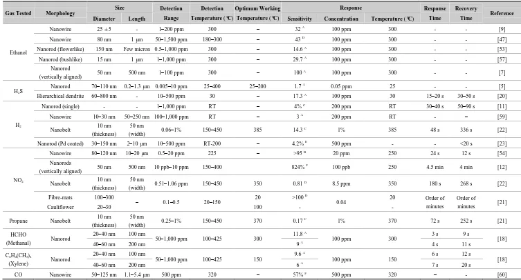
Table 3. Summary of the gas sensing properties of 1-D ZnO nanostructures for different gases.
Gas Tested Morphology
Size Detection
Range
Detection
Temperature (°C)
Optimum Working
Temperature (°C)
Response Response
Time
Recovery
Time Reference
Diameter Length Sensitivity Concentration Temperature (°C)
Ethanol
Nanowire 25 ± 5 - 1–200 ppm 300 – 32 A 100 ppm 300 - - [9]
Nanowire 80 nm 1 µm 50–1,500 ppm 180–300 – 43 D 100 ppm 300 - - [47]
Nanorod (flowerlike) 150 nm Few micron 0.5–1,000 ppm 300 – 14.6 A 100 ppm 300 - - [53]
Nanorod (bushlike) 15 nm 1 µm 1–1,000 ppm 300 – 29.7 A 100 ppm 300 - - [57]
Nanorod
(vertically aligned) 50 nm 500 nm 1–100 ppm 300 – 100
A 100 ppm 300 - - [7]
H2S
Nanorod 70–110 nm 0.2–1.3 µm 0.005–10 ppm 25–400 25–200 1.7 A 0.05 ppm 25 - - [5]
Hierarchical dendrite 60–800 nm - 10–500 ppm 30 – 17.3 A 100 ppm 30 15–20 s 30–50 s [20]
H2
Nanorod (single) - - 1–1,000 ppm RT – 4% C 200 ppm RT 30–40 s 50–90 s [11]
Nanowire 10–30 nm 50–250 nm 100–1,000 ppm RT – 3 A 200 ppm RT - – [59]
Nanobelt 10 nm (thickness)
50 nm
(width) 0.06–1% 150–450 385 14.3
C 1% 385 48 s 336 s [22]
Nanorod (Pd coated) 30–150 nm 2–10 µm 10–500 ppm RT-200 – 4.2% E 500 ppm - - <20 s [23]
NO2
Nanowire 80–120 nm 10–20 µm 0.5–20 ppm 225 – >95 B 20 ppm 250 24 s 12 s [54]
Nanorods
(vertically aligned) 50 nm 500 nm 10 ppb–10 ppm 150–400 824%
F 100 ppb 250 4.5 min 4 min [12]
Nanobelt 10 nm (thickness)
50 nm
(width) 0.51–1.06 ppm 150–450 350 0.81
D 8.5 ppm 350 180 s 268 s [22]
Fibre-mats 100–300
– 0.1–0.5 20–150 20 >100
D
0.04 20 Order of
minutes
Order of
minutes [21]
Cauliflower 20–30 100 - -
Propane Nanobelt 10 nm (thickness)
50 nm
(width) 0.25–1% 150–450 370 0.17
C
1% 370 72 s 252 s [21]
HCHO
(Methanal) Nanorod
20–40 nm 100 nm
50–1,000 ppm 100–425 300 11.8
A
100 ppm 300 3 s 9 s [18]
40–60 nm 200 nm 9 A 4 s 11 s
C6H4(CH3)2
(Xylene) Nanorod
20–40 nm 100 nm
50–1,000 ppm 100–425 150 9.6
A
100 ppm 150 6 s 12 s [18]
40–60 nm 200 nm 6 A 7 s 20 s
CO Nanowire 50–125 nm 1.1–5.4 µm 500 ppm 320 – 57% F 500 ppm 320 – - [60]
1-D ZnO nanostructures have been reported to have a very poor response to CO, O2, and CH4 gases at room temperature [11]. Hsueh et al. [47] measured the sensitivity of ZnO nanowires having different diameters and length for CO sensing. It was seen that thinner and taller ZnO nanowires could detect CO gas more efficiently compared to wider and shorter nanowires. For example, at 320 °C, ZnO nanowires having diameter of 50–70 nm and length of 5.4 µm had a response of 57% at 500 ppm CO concentration. This variation in the result from Hsueh et al. [47] and Lupan et al. [11] could be attributed to the difference in detection temperature used in the study. Hsueh et al. [47] measured the sensitivity towards CO at 320 °C, whereas Lupan et al. [11] measured the sensitivity at room temperature.
Sensitivity of ZnO nanorods towards methanol (HCHO) and xylene (C6H4(CH3)2) was investigated by Cao et al. [18]. ZnO nanorods exhibited good sensitivity to HCHO and C6H4(CH3)2 at low working temperatures. Nanorods having smaller dimensions (length: 100 nm, diameter: 20–40 nm) exhibited higher sensitivity compared to nanorods having larger dimensions (length: 200 nm, diameter: 40–60 nm). It was claimed that the higher sensitivity in the smaller nanorods was due to the increased surface area as seen in Table 3.
ZnO nanostructures also show a good response towards hydrocarbons such as methane [5] and propane [11,22]. The optimum working temperature evaluated for propane was 370 °C with a response and recovery time of 72 s and 252 s, respectively. The sensitivity towards propane was not as high as other target gases but still, the results showed a promising response for industrial applications. The response of ZnO nanobelts towards 1% propane at 370 °C was 0.17. The response of ZnO nanorods towards methane was further lower and found to be only 0.002 at room temperature [11].
Gas sensing properties of one-dimensional ZnO nanorods exhibit improved response and stability than those of ZnO nanoparticles [61]. Previously, it was demonstrated that uniform ZnO nanorods can be used to improve the response of ZnO based gas sensors to H2 gas [23,61]. However, the Pd-coated ZnO nanowires gas sensors reported by Wang et al. showed a higher H2 sensitivity (4.2%) and fast response and recovery time at concentrations up to 500 ppm at room temperature [62]. In general, it can be said that 1-D ZnO nanostructures can detect ethanol and H2S gas most efficiently. The sensitivity of 1-D ZnO nanostructures towards other gases such as H2, NO2, CO, O2, hydrocarbons is comparatively low without additional functionalization by catalyst doping. The response and recovery times show a direct dependence on the target gas. The performance of the sensors depends greatly on the morphology of 1-D ZnO nanostructures and the operating temperature used.
4.2. 1-D SnO2 Nanostructured Gas Sensors
4.2.1. Growth and characterization of SnO2 Nanostructures
Few reports of the production of SnO2 nanostructures by hydrothermal methods have been reported as compared to ZnO. However, Lupan et al. [63] reported an inexpensive and rapid fabrication technique for rutile SnO2 nanowires/nanoneedles at a low temperature by a hydrothermal method without the use of seeds, templates or surfactants. A solution containing SnCl4·5H2O, NH4(OH) was employed for the growth of SnO2 nanowires/nanoneedles at 95–98 °C on Si/SiO2 substrates. Individual nanowires can be easily transferred to other substrates for fabricating single nanowire ultrasensitive sensors [11]. The resulting nanowires/nanoneedles have a diameter of approximately 100 nm with lengths of 10–20 µm. The morphology, dimension and aspect ratio of nanowires are a function of growth time, temperature and Sn4+/OH− ratio in solution. Thinner nanowires can be produced by decreasing the concentration of SnCl4 in solution. When the ratio between SnCl4 and NH4OH was as high as 1:20, long tetragonal square-based nanowires were obtained. Experimental results showed that the molar ratio of 1:20 made the hydrolysis occur rapidly due to a higher quantity of nuclei. By further increasing the ratio above 1:30 no nanowires were formed. Similarly, Shi et al. [64] produced SnO2 nanorods by hydrothermal process and then loaded the nanorods with La2O3 by simple chemical method. The SnO2 nanorods were synthesized from the precursors SnCl4-5H2O and NaOH at 190 °C in an alcohol/water solution. La2O3 was then loaded on the SnO2 nanorods by dispersing the nanorods in alcohol followed by the addition of La(NO3)3-6H2O solution.
Qi et al. [13] grew SnO2 nanofibers by the electrospinning technique. In this process, SnCl2 was mixed with N,N-dimethylformamide (DMF) and ethanol subsequently adding poly(vinyl pyrrolidone) (PVP) under vigorous stirring. Then the mixture was loaded into a glass syringe with a 10 kV power supply between the cathode and anode. The conversion of SnCl2 to SnO2 and the removal of PVP were achieved by calcining at 600 °C for 5 h in air. Choi et al. [65] also produced Pd doped SnO2 hollow nanofibers by single capillary electrospinning process. In this procedure SnCl2-2H2O was dissolved in mixed solvents of ethanol and N,N-dimethylformamide followed by stirring and addition of PVP. After stirring for 10 h, a clear solution was obtained and used for the preparation of undoped SnO2 nanofibers. For the fabrication of Pd-doped SnO2 nanofibers, PdCl2 was added to the solution. The solution was loaded in a plastic syringe and electrospun by applying 20 kV at an electrode distance of 10 cm. The as-spun fibers were heat treated at 600 °C for 2 h to convert into undoped or Pd-doped SnO2 nanofibers. Dong et al. [56] also developed Pt doped SnO2 nanofibers by electrospinning with a similar procedure as that reported by Choi et al. and as seen in Figure 7(a) [65]. After synthesis of the SnO2 nanofibers, PtCl4 was added to the solution and loaded in a plastic syringe followed by electrospining at a voltage of 20 kV with 10 cm electrode distance. The as-spun fibers were heat treated at 600 °C for 2 h.
ZnO nanorods were also prepared by molten-salt method where SnO2 powder was mixed with NaCl and a nonionic surfactant [16]. The mixture was heated in a porcelain crucible at 800 °C in an electric furnace followed by cooling, washing in distilled water, filtering and drying. It was claimed that addition of the nonionic surfactant formed a shell surrounding the SnO2 particles to prevent agglomeration and ensured uniform nanorods.
resulting nanofibers had 100–200 nm diameters. Increasing the exposure time to the gas mixture resulted in an increase in the average nanofiber length. It was found by further investigations that the presence of Au nanoparticles was essential to assist the growth of nanofibers. Direct oxidation is another solid-state processing route where SnO2 nanoribbons (Figure 7(b)) were grown at 810 °C from Sn powders in the presence of Ar gas flow [27]. To modify the surface of SnO2 nanoribbons, CuO was introduced to the nanoribbons by mixing SnO2 and CuO in distilled water.
Figure 7. Scanning electron microscopy (SEM) images of (a) SnO2 nanofibers produced by electrospinning after heating at 600 °C for 2 h [56]. (b) SnO2 nanoribbons synthesized by direct oxidization [27]. (c) On-chip fabrication of SnO2 nanowires grown on Au deposited Pt interdigitated substrate by thermal evaporation [10]. (d) SnO2-ZnO hybrid nanofiber by electrospinning [67].
[image:15.595.148.449.286.496.2]deposited on an alumina plate by thermal evaporation process at 1,000 °C by using SnO powder and Ar gas at 300 Torr pressure and without using any catalyst [37]. The deposited SnO2 nanobelts were retrieved from the alumina substrate and separated into individual nanobelts in an isopropyl alcohol solution via ultrasonic agitation.
[image:16.595.52.545.314.789.2]A hybrid process was also reported for the production of mixed SnO2-ZnO composite oxide nanostructures [67]. For this preparation, Zn(CH3COO)·2H2O was mixed with poly(4-vinylphenol) and stirred for 3 h at 60 °C followed by addition of ethanol. The solution was then loaded into a plastic syringe with a voltage supply of 7 kV. The substrate temperature was maintained at 80 °C. The as-prepared ZnO nanofibers were collected on Pt interdigitated SiO2/Si substrate and calcined at 600 °C. The SnO2 was deposited on the ZnO nanofibers using pulsed laser deposition (PLD) method with KrF excimer laser (λ = 248 nm). A scanning electron microscopy (SEM) micrograph of SnO2-ZnO nanofibers is shown in Figure 7(d).
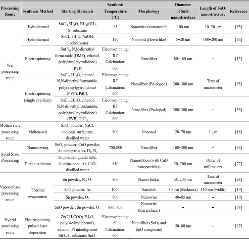
Table 4. Summary of various processing routes for the production of 1-D SnO2 nanostructures. Processing
Route Synthesis Method Starting Materials
Synthesis Temperature
(°C)
Morphology
Diameter of SnO2
nanostructure
Length of SnO2
nanostructure Reference
Wet processing
route
Hydrothermal SnCl4.5H2O, NH4(OH),
Si substrate 95 Nanowires/nanoneedle 100 nm 10–20 µm [63] Hydrothermal SnCl4.5H2O, NaOH,
alcohol/water 190 Nanorod (flowerlike) 5–20 nm 100–200 nm [64]
Electrospinning
SnCl2, N,N-dimethyl
formamide (DMF), ethanol, poly(vinyl pyrrolidone) (PVP) Electrospinning: RT Calcination: 600
Nanofiber 80–160 nm – [13]
Electrospinning (single capillary)
SnCl2.2H2O, ethanol,
N,N-dimethylformamide, poly(vinylpyrrolidone)
(PVP), PdCl2
Electrospinning: RT Calcination:
600
Nanofiber(Pd-doped) 200–300 nm Tens of
micrometer [65]
SnCl2.2H2O, ethanol,
N,N-dimethylformamide, poly(vinyl pyrrolidone)
(PVP), PtCl4
Electrospinning: RT Calcination:
600
Nanofiber(Pt-doped) 200–300 nm – [56]
Molten-state processing
route
Molten-salt
SnO2 powder, NaCl,
nonionic surfactant, distilled water
800 Nanorod 20–70 nm 1 µm [16]
Solid-State Processing
Nanocarving SnO2 powder, CoO powder, Au nanoparticles, H2, N2
700-800 Nanofiber 100–200 nm – [66]
Direct oxidation
Sn powder, quartz tube, alumina boat, Ar, CuO,
distilled water
810 Nanoribbon (with CuO
nanoparticles) 20–200 nm
Order of
millimeters [27]
Vapor-phase processing
route
Thermal evaporation
Sn powder, N2, O2 800 Nanowhisker 50-200 nm
Tens of
micrometer [28] SnO powder, Ar 1000 Nanobelt 80 nm (thickness) 330 nm (width) [10]
Sn powder, O2 800 Nanowire 40–85 nm – [10]
SnO powder, Sn powder, O2 980, 800
Nanowire
(hierarchical) – – [68]
Hybrid processing route Electrospinning, pulsed laser deposition
Zn(CH3COO)·2H2O,
poly(4-vinyl phenol), ethanol, Pt interdigitated
SiO2/Si substrate, SnO2
Electrospinning: 80 Calcination:
600
Nanofiber (SnO2 and
Among the synthesis methods, thermal evaporation and electrospinning are the most commonly employed methods for the production of SnO2 nanostructures. The nanostructures obtained by hydrothermal and electrospinning processes are nanorods and nanofibers, respectively. The processing temperature in the molten-salt processing route is 800 °C and produced nanorods. However, presence of Au catalyst is essential during vapor-assisted growth process for the production of SnO2 nanofibers. In the thermal evaporation process, heat (800–980 °C) and pressure are involved and a variety of nanostructures could be obtained including nanowires (normal, hierarchical), nanobelts and nanowhiskers. In this synthesis method, SnO2 nanostructures grow only in the presence of Au catalyst. A summary of the various processing routes is presented in Table 4.
4.2.2. Sensing Performance of SnO2 1-D Nanostructures
In the reported literatures, the sensitivity of SnO2 nanostructures was evaluated for different target gases such as ethanol, H2S, H2, NH3, liquefied petroleum gas (LPG), toluene, acetone and triethylamine. The morphology of the nanostructures employed for sensing included nanorods (normal, flowerlike), nanowires (normal, hierarchical), nanofibers, nanobelts and nanowhiskers. Sensitivity, response time, recovery time and optimum detection temperature were considered to evaluate the sensing performance.
Ying et al. [28] synthesized SnO2 nanowhiskers by thermal evaporation for ethanol sensing. The sensitivity of SnO2 nanowhiskers was 23 upon exposure to 50 ppm ethanol at 300 °C. The recovery time was about 10 min. Nanorods with a flowerlike morphology developed by Shi et al. [64] had a response of 45.1 at 200 °C for 100 ppm ethanol concentration. The response was further increased by developing La2O3 loaded SnO2 nanorods with a flowerlike morphology by Shi et al. [64]. It was seen that the sensitivity of 5 wt% La2O3 loaded SnO2 nanorods had a response of 213 whereas without loading had only 45.1 at 200 °C for 100 ppm ethanol concentration. The increased sensitivity with the loading of 5 wt% La2O3 on SnO2 nanorods was explained by the basic nature of La2O3. The presence of La2O3 reduces the acidic sites and leads to increase in the dehydrogenation process [69,70]. As a result, many more CH3CH2OH molecules convert to CH3CHO due to the presence of La2O3 which creates a favorable condition to convert to CO2 and H2O from the thermodynamic point of view [71]. Choi et al. [65] showed significantly different responses towards C2H5OH with Pd doping on SnO2 hollow nanofibers. Selective detection of C2H5OH was observed with the doping of Pd on SnO2 hollow nanofibers. In 0.4 wt% Pd-doped SnO2 hollow nanofibers, the response to 100 ppm C2H5OH was 1,020.6 at 330 °C, whereas CH4, CO, H2 had very negligible responses. However, the response of C2H5OH decreased dramatically as the sensor temperature was increased from 330 to 440 °C, while response to CH4 and H2 was increased or only varied only slightly. Therefore, the selective detection of H2 and/or CH4 was optimized at 440 °C with the minimum interference to C2H5OH. The selective gas sensing was explained in terms of the different catalytic oxidation activities of the analyzed gases as a function of sensor temperature and Pd doping concentration. The response time was evaluated to be <10 s for this sensor but the recovery time was higher at about 503 s for 100 ppm C2H5OH at 385 °C. The slow recovery was explained by the sluggish surface reactions of adsorption, dissociation, and ionization of oxygen. It was found that with increase in temperature the recovery time decreased.
decrease with an increase in temperature from 300 to 500 °C. For SnO2 nanofibers, the response time varied between 2 and 7 s and the recovery time varied between 267 and 281 s. However, the sensitivity of the SnO2 sensors could be further increased by Pt doping [56]. The doping of 0.08 wt% of Pt on SnO2 nanofibers produced a response of 5,100 for 20 ppm H2S gas at 300 °C. The response time of Pt doped SnO2 nanofibers was found to be faster (1 s) compared to undoped SnO2 nanofibers (2–7 s). The surface modification due to the Pt doping increased the resistance of the nanofibers which indicated higher grain barriers. Increased resistance in the grain barrier might be due to a higher oxygen adsorption introduced by the presence of Pt, or may be directly related to the presence of a Pt catalyst at the grain surface [72,73]. SnO2 nanoribbons in presence of CuO nanoparticles showed a sensitivity of 18,000 towards H2S gas at 50 °C [27]. Presence of CuO nanoparticles formed n-p junction in the nanoribbons network. However, existence of H2S gas forms a thin CuS layer on CuO nanoparticles, which is a good conductor. As a result, the n-p hetero-junction was converted into a Schottky barrier which induced a remarkable change in the sensitivity.
Fields et al. [74] developed a SnO2 nanobelt-based sensor for H2 detection. It was found that the sensitivity of SnO2 nanobelts at 25 °C was 60% and remained nearly constant up to 80 °C for 2% H2 concentration. It was found that both the response and recovery times were about 220 s at 25 °C. It was also found that when the temperature was increased to 80 °C, the response time decreased to about 60 s, while the recovery time increased to about 500 s. The relatively long response time is believed to be caused by the low chemical reaction rate. It is likely that the response can be improved by coating the nanobelt surface with a catalyst such as Pd or Pt in order to produce a practical room-temperature H2 sensor.
The length of SnO2 nanowires had an impact on the sensor’s performance for detecting NH3. Longer nanowires showed higher sensitivity toward NH3 gas compared to shorter nanowires. The response to 1,000 ppm NH3 at an operating temperature of 200 °C varied from 3 to17 with varying the nanowire length from 40–85 nm [10]. It was observed that hierarchical nanowires showed higher response towards NH3 compared to the normal nanowires. For 1,000 ppm NH3 concentration at 200 °C, the response of hierarchical nanowires was found to be 21.7 [68], whereas the response of normal nanowires was 11 [10].
Like NH3, the response of SnO2 nanowires towards liquefied petroleum gas (LPG) depends on the length of the nanowire. Longer nanowires exhibit an increased response compared to shorter nanowires. In the experiments of Thong et al. [10], the response of SnO2 nanowires increased from 1.5 to 21.8 when the length of the nanowire was increased from 40 to 85 nm at 350 °C for 2,000 ppm LPG. The optimum working temperature was determined to be 350 °C with a response and recovery time of less than 10 s. Comparing the response of hierarchical nanowires with normal nanowires, it was seen that the sensitivity towards LPG was increased three times at the optimal operating temperature [68]. It was found that the response of normal SnO2 nanowires (length 60 nm) for 2,000 ppm LPG was 5.8 [10], whereas the response of hierarchical SnO2 nanowires was 20.4 at 350 °C [68].
Table 5. Summary of the gas sensing properties of 1-D SnO2 nanostructures for different gases.
Gas Tested Morphology Size Detection Range Detection
Temperature (°C)
Optimum Working
Temperature (°C)
Response Response
Time
Recovery
Time Reference
Diameter Length Sensitivity Concentration Temperature (°C)
Ethanol
Nanowhisker 50–200 nm Tens of
micrometers 50 ppm 300 – 23
A 50 ppm 300 – 10 min [28]
Nanorod (flowerlike) 5–20 nm 100–200 nm 10–1,000 ppm 200, 300 200 45.1 A 100 ppm 200 – – [64]
Nanorods (flowerlike loaded with La2O3)
5–20 nm 100–200 nm 10–1,000 ppm 200, 300 200 213 A 100 ppm 200 – – [64]
Nanofiber (Pd doped) 200–300 nm Tens of
micrometers 100 ppm 330–440 330 1,020.6
A 100 ppm 330 <10 s 503 s for 100
ppm at 385 °C [65]
H2S
Nanofiber 200–300 nm – 4–20 ppm 300–500 300 121 A 20 ppm 300 2–7 s
267–281 s for 200 ppm
at 400 °C
[56]
Nanofiber (Pt doped) 200–300 nm – 4–20 ppm 300–500 300 5,100 A 20 ppm 300 1 s
214–267 s for 200 ppm
at 400 °C
[56]
Nanoribbon (loaded
with CuO nanoparticles) 20–200 nm
Order of
millimeters 3 ppm 27–200 50 18,000
A 3 ppm 50 – – [27]
H2 Nanobelts
80 nm
(thickness) 330 nm (width) 2% 25–80 – 60%
C 2% 25 220 s
at 25 °C
220 s at
25 °C [74] NH3
Nanowire 60 nm – 300–1,000 ppm 50–300 200 11 A 1,000 ppm 200 – – [10]
Nanowire (hierarchical) 60 nm – 300–1,000 ppm 50–300 200 21.7 A 1,000 ppm 200 – – [68]
LPG Nanowire 60 nm – 500–2,000 ppm 50–450 350 5.8
A 2,000 ppm 350 <10 s at
350 °C
<10 s at
350 °C [10]
Nanowire (hierarchical) 60 nm – 500–2,000 ppm 50–450 350 20.4 A 2,000 ppm 350 – – [68]
Toluene Nanofiber 80–160 nm – 10–10,000 ppm 310–380 350 6 A 100 ppm 350 1 s 5 s [13]
Acetone Nanorod 20–70 nm 1 µm 1–100 ppm 450 450 3.7 A 10 ppm 450 – – [16]
Triethylamine Nanorod 20–70 nm 1 µm 1–100 ppm 350 350 64.8 A 50 ppm 350 <10 s <10 s [16]
NO2
Nanofiber (SnO2-ZnO
composite) 55–80 nm – 0.4–3.2 ppm 150–300 180–200 105
B 3.2 ppm 200 – – [67]
Composite nanofibers of SnO2 and ZnO were exposed to various NO2 concentrations by Park et al. [67]. The optimum sensitivity of the SnO2-ZnO composite nanofiber was found to be between 180–200 °C operating temperatures. The sensitivity for 3.2 ppm NO2 was 105 at 200 °C. High sensitivity towards NO2 forthe SnO2-ZnO composite nanofibers was reportedly due to two factors: the increased adsorption due to nanocrystalline SnO2 coating and the charge transfer occurring between SnO2 and ZnO.
From the review of reported literature, it can be surmised that SnO2 nanostructure-based sensors were developed with reasonable success for detecting a range of gases including ethanol, H2S, H2, NH3, liquefied petroleum gas (LPG), toluene, acetone, NO2 and triethylamine. However, the sensitivity and selectivity can be further improved by doping (Pd and Pt), adding nanoparticles (CuO), loading (La2O3), and morphological modifications (hierarchical nanowires). Additionally, preparation of composite nanostructures (SnO2-ZnO nanofiber) also improves the sensitivity and selectivity of the sensors. Unlike ZnO nanostructures, the response and recovery times of the SnO2 nanostructures show a strong dependence on the operating temperature. The optimum operating temperature is of vital importance since by simply adjusting the operating temperature, SnO2 sensors can be used for selective gas sensing. A summary of SnO2 nano-structured sensor performance is presented in Table 5.
4.3. 1-D TiO2 Nanostructured Gas Sensors
4.3.1. Growth and Characterization of TiO2 Nanostructures
The processing routes for the synthesis of 1-D TiO2 nanostructures can be divided into two groups: (i) wet processing routes and (ii) solid-state etching. Most commonly wet processing route is employed for the synthesis of 1-D TiO2 nanostructure. The wet processing route includes hydrothermal, electrospinning and anodization. Nanocarving by H2 gas, UV lithography and dry plasma etching fall under solid-state etching process. Depending on the processing routes and conditions different surface morphologies such as nanotube arrays, branched nanotubes, coated nanotubes, nanoparticle added nanotubes, nanobelts, nanofibers and nanowires of TiO2 can be obtained. The crystal structure also can be changed by annealing. The processing details for the growth of 1-D TiO2 nanostructures are summarized in Table 6.
TiO2 nanobelts via an alkaline hydrothermal process by using commercial TiO2 powders, NaOH, HCl, and deionized water. The obtained H2Ti3O7 nanobelts were annealed at 600 °C for 1 h to obtain crystalline TiO2 nanobelts. The surface of the TiO2 nanobelts was coarsened by adding H2SO4 into H2Ti3O7 aqueous solution under magnetic stirring followed by heating at 100 °C for 12 h. The powder was washed and annealed at 600 °C for 1 h to obtain surface-coarsened TiO2 nanobelts. For the preparation of Ag nanoparticle-TiO2 nanobelts and surface coarsened Ag nanoparticel-TiO2 nanobelts, the hydrothermal process was combined with a photocatalytic reduction process [38]. The as-prepared TiO2 nanobelts obtained by hydrothermal route were dispersed into AgNO3 and ethanol solution. The solution was illuminated with a 20 W ultraviolet lamp under magnetic agitation. The obtained phase of TiO2 nanobelt was anatase.
Landau et al. [76] synthesized TiO2 nanofibers by electrospinning. The electrospun solution comprised of poly(vinyl acetate) (PVA), dimethylformamide (DMF), titanium (IV) propoxide, and acetic acid in an electric field of 1.5 KV/cm. The solution was electrospun at room temperature on wax paper or Si wafer rotating at 100 rpm. It was seen that the morphology of the nanofiber depended on the concentration of PVA. At low concentration (≤2 wt%) the network comprised of small beads interconnected by thin fibers whereas at higher concentration (≥5 wt%) the beads disappeared and the fiber became continuous and homogeneous. The diameter of the nanofibers was seen to increase from 120 nm to 850 nm with an increase in the polymer concentration from 5 wt% to 12 wt%.
To prepare Cu-doped TiO2 nanofibers by electrospinning tetrabutyl titanate was mixed with acetic acid and ethanol under vigorous stirring for 10 min [50]. Subsequently, this solution was added to ethanol containing PVP and CuCl2-2H2O under vigorous stirring for 30 min. Then, the mixture was loaded into a glass syringe and connected to a high-voltage power supply of 12 kV over a distance of 20 cm between the electrodes. The conversion of tetrabutyl titanate to TiO2 and the complete removal of PVP were achieved by calcining at 500 °C for 3 h in air. It was found from the XRD analysis that the crystallographic phases were 20% anatase and 80% rutile with a nanofiber diameter of 80 nm.
amorphous TiO2 nanotube arrays were annealed at 450 °C in air for 2 h to obtain anatase TiO2. The resulting nanostructure had an outer and inner diameter of 150 nm and 110 nm, respectively with length of approximately 2.3 µm. The nanotube dimension could be varied in the anodization process by changing both the pH of the electrolyte and the electrode voltage [79]. In the work of Paulose et al. [79] nanotube arrays were prepared by anodization of 250 µm thick titanium foils in an electrolyte containing sodium hydrogen sulfate monohydrate, potassium fluoride and sodium citrate tribasic dihydrate (Figure 8(b)). The pH of the electrolyte was adjusted by the addition of sodium hydroxide. It was seen that the pore diameter depended on the anodization voltage, whereas the nanotube length depended on both the electrolyte pH and anodization voltage. Nanotube lengths varied from 380 nm to 6 µm and pore diameters from 30 to 110 nm as the electrolyte pH (1.11–5) and the anodization potential (10–25 V) was changed. The as-prepared amorphous samples were crystallized by annealing at temperatures ranging from 370 to 630 °C in oxygen for 6 h.
[image:22.595.104.491.355.508.2]Figure 8. (a) Transmission electron microscopy (TEM) image of Pt nanoparticles added TiO2 nanotubes [75]. (b) Scanning electron microscopy (SEM) micrograph of the top view of the TiO2 nanotube array grown by anodization process [79].
Table 6. Summary of various processing routes for the production of 1-D TiO2 nanostructures.
Processing
Route
Synthesis
Method Starting Materials
Crystal
Structure
Synthesis
Temperature
(°C)
Morphology
Diameter
of TiO2
nanostructure
Length of TiO2
nanostructure Reference
Wet processing route
Hydrothermal
TiCl3, HCl, NaCl, deionized
water, alcohol
Rutile 200 Nanowire 20–80 nm 100–800 nm [59]
TiO2 powders, PdCl2, H2PtCl6,
NaOH, HCl, deionized water Lepidocrocite 150
Nanotube (with Pd/Pt nanoparticles)
100 nm - [75]
TiO2 powders, NaOH, HCl,
deionized water Anatase 600 Nanobelt
50 nm (thickness)
100–150 nm (width) [38]
Hydrothermal, Photocatalytic reduction
TiO2 powders, NaOH, HCl,
deionized water, AgNO3 ethanol
solution
Anatase 600
Nanobelt (with Ag nanoparticles)
50 nm (thickness)
100–150 nm (width) 10–30 nm (Ag nanoparticles)
[image:22.595.50.547.542.756.2]Table 6.Cont.
Processing
Route
Synthesis
Method Starting Materials
Crystal Structure Synthesis Temperature (°C) Morphology Diameter
of TiO2
nanostructure
Length of TiO2
nanostructure Reference
Wet processing
route
Electrospinning
poly(vinyl acetate) (PVA), dimethylformamide (DMF), titanium (IV) propoxide, acetic
acid
Anatase RT Nanofiber 120–850 nm - [76]
Tetrabutyl titanate, acetic acid, ethanol, poly(vinyl pyrrolidone)
(PVP), CuCl2.2H2O
Anatase, rutile, brookite
500 Nanofiber 80 nm - [50]
Anodization
Titanium foil, platinum foil, hydrofluoric acid, water
Anatase,
Rutile 500
Nanotube
array 46–76 nm 400 nm [44] Titanium foil, platinum foil,
NH4F, (NH4)2SO4, deionized
water.
Amorphous 450
Nanotube
array 150 nm 2.3 µm [78]
Titanium foils, sodium hydrogen sulfate monohydrate, potassium fluoride, sodium citrate tribasic dehydrate, sodium hydroxide
- 370-630
Nanotube
array 30–110 nm 380 nm −6 µm [79]
Titanium foil, acetone, isopropanol, platinum foil, NH4F,
dimethyl sulphoxide
Anatase 400 Nanotube
array 350 nm 3.5 µm [14]
Anodization, hydrothermal
Titanium foil, acetone, isopropanol, platinum foil, NH4F,
dimethyl sulphoxide, HCl, titanium (IV) isopropoxide,
ethanol
Anatase 400
Nanotube (branched array)
350 nm 3.5 µm [14]
Titanium foil, acetone, isopropanol, platinum foil, NH4F,
dimethyl sulphoxide, P25, distilled water
Anatase 400
Nanotube array (P25 coated)
350 nm 3.5 µm [14]
Solid-state etching
Nanocraving
TiO2 powder, H2, N2 Rutile 700 Nanofiber 15–50 nm 1–5 µm [80]
TiO2 powder, mixed oxide of TiO2
and SnO2 powder, isopropanol,
H2, N2
Rutile 700 Nanofiber 5–10 nm 0.2–1 µm [25]
Solid-state etching
UV lithography, dry plasma
etching
TiO2, positive photoresist, silicon
substrate Anatase 500 Nanowire 90-–180 nm 1400 µm [26]
with a wall thickness of 10 nm. The branched TiO2 nanotubes were obtained through a modification process on TiO2 nanotubes array by hydrothermal methods [14]. The as prepared TiO2 nanotube arrays were immersed in a solution containing HCl with constant stirring at 25 °C for 15 min. Titanium (IV) isopropoxide was dropped into the solution under constant stirring for 1 h, and then the beaker was sealed and heated at 95 °C for 9 h with slight stirring. After the reaction, the reactant was cooled to room temperature and washed with ethanol and distilled water. The as prepared branched TiO2 nanotube arrays were annealed in a muffle furnace at 400 °C for 2 h. It was observed that TiO2 nanocrystal nucleus formed on the rough surfaces of the TiO2 nanotubes with special bamboo structures with a larger and rougher surface area. Similarly, P25 (A commercial photocatalyst from Degussa, Germany) coated TiO2 nanotube arrays were synthesized by the hydrothermal approach on the uncoated TiO2 nanotube arrays [14]. In this process P25 was added to distilled water and then mixed vigorously by magnetic stirring and ultrasonicating followed by transferring into a Teflon-lined autoclave. The autoclave was sealed and heated to 80–120 °C for 12 h to coat P25 on the TiO2 nanotube arrays, and then it was cooled to room temperature and washed with distilled water. The P25 coated TiO2 nanotube arrays were annealed at 400 °C for 2 h.
A novel approach was developed for the production of nanofibers of pure TiO2 and mixed oxide of TiO2 and SnO2 through a nanocarving process [25,80]. Pure TiO2 nanofibers were produced by sintering TiO2 nanoparticle (32 nm) pellets formed at 392 MPa in a temperature range from 1,100–1,400 °C [80]. The sintered TiO2 was shaped as a disk with a thickness of 1 mm and diameter of 10 mm that was exposed to an atmosphere of 5% H2 with balance N2 at 700 °C. Two types of gas flow rates (100 and 500 mL/min) were studied. It was found that samples sintered at 1,200 °C with a gas flow rate of 500 mL/min showed well developed fiber with a diameter of 15–50 nm and length of 1–5 µm. Similarly, for mixed oxide nanofibers, 90 mol% TiO2 and 10 mol% SnO2 powder was mixed in isopropanol followed by milling with yttria stabilized zirconia balls for 4 h [25]. After ball milling, the isopropanol was evaporated and the resulting powders were compacted into 12.7 mm disks at a peak stress of 392 MPa. The compacted disks were then sintered at two different temperatures, 1,450 °C and 1,200 °C for 2 and 6 h respectively. To create nanofibers, the sintered disks were exposed to 5% H2 in background N2 at 700 °C for 8 h under approximately 1,000 mL/min flow of gas. From XRD results it was seen that the TiO2–SnO2 mixture sintered at 1,450 °C represented only rutile and SnO2 was completely dissolved (solid solution) into the TiO2 matrix. On the other hand, SnO2 peaks were found for the TiO2–SnO2 samples sintered at 1,200 °C, which indicated that the mixture went through spinodal decomposition. During the nanocarving process for 2 h in the solid solution sample nanofibers were not evident. However, for the 6 h solid solution samples, nanofibers were obvious and grains become faceted. From this, the authors claimed that faceted grains with rutile structure were beneficial for nanofiber formation. The spinodally decomposed samples nanocraved for 6 h had well defined and oriented fibers with grooves on the grains which ensured enhanced surface area.
Plasmalab 80 RIE reactor to perform micromachining of TiO2 thin films at 200 mTorr and SF6 chemistry. The etching time was about 390 s. The resulting nanowire arrays were 90–180 nm in width and 1,400 µm in length.
Among the processing routes for the production of TiO2 nanostructures, the hydrothermal and anodization approaches are most commonly employed. Depending on the starting materials and process conditions, the crystal structure of TiO2 nanostructures varied from anatase, rutile, brookite and tolepidocrocite. It was also seen that the morphology of the nanostructures can be altered by combining two processes. As an example, branched nanotubes can be obtained by the combination of anodization and hydrothermal processes. It is also seen that the anodization voltage has an effect on the pore diameter and pH has effect on the length and diameter of the nanostructure. Generally, with an increase in the anodization voltage and pH, the diameter and length of the nanostructure also increase. The as-grown nanostructures produced by anodization are mostly nanotube arrays with an amorphous crystal structure. However, annealing can be performed (>400 °C) to crystallize the nanostructure to either anatase or rutile. The H2-etching of TiO2 (nanocarving process) is a novel approach and provides an avenue for gas-phase assisted nano-machining of ceramics.
4.3.2. Sensing Performance of TiO2 1-D Nanostructures
Varghese et al. [44] grew TiO2 nanotubes arrays on Ti foil by an anodization process. The TiO2 nanotubes exhibited anatase phase at the nanotube walls and rutile phase at the barrier layer. They were able to detect H2 at temperatures as low as 180 °C. TiO2 nanotubes with a smaller pore diameter (46 nm) had higher sensitivity compared to larger pore diameters (76 nm) towards H2 gas. Generally, the sensitivity of TiO2 nanotubes increased with increasing temperature showing a variation of three orders in magnitude of resistance to 1,000 ppm of H2 at 400 °C. Conversely, the response time decreased with increasing temperature. It was seen that at 290 °C the response time was approximately 3 min. The sensors showed high selectivity to H2 compared to CO, CO2 and NH3. The high sensitivity of the nanotubes was due to H2 chemisorption onto the TiO2 surface where they acted as electron donors. TiO2 nanotube arrays (pore diameter 30 nm, wall thickness 13 nm, length ~1 µm) having a crystalline structure showed the highest resistance variation, 8.7 orders of magnitude for 1,000 ppm H2 [79]. The ultra high response of this sensor is believed to be due to the highly active surface states on the nanotube walls, high surface area of the nanotube architecture, and the ordered geometry of the tube to tube electrical connections. Rout et al. [59] synthesized TiO2 nanowires with rutile structure for the detection of H2 gas at room temperature in presence of dry air. It was seen that at room temperature TiO2 nanowire showed sensitivity of 8 at 1,000 ppm H2 concentration.

![Figure 4. Schematic illustration of a tube-type 1-D nanostructured gas sensor [31].](https://thumb-us.123doks.com/thumbv2/123dok_us/8649090.867148/5.595.143.452.407.503/figure-schematic-illustration-tube-type-nanostructured-gas-sensor.webp)


![Figure 5. ZnO nanostructures. (a) Randomly distributed nanorods produced by hydrothermal process [48]](https://thumb-us.123doks.com/thumbv2/123dok_us/8649090.867148/8.595.148.448.159.425/figure-nanostructures-randomly-distributed-nanorods-produced-hydrothermal-process.webp)
![Figure 6. Resistivity of n-type ZnO sensor is decreased when exposed to reducing ethanol environment [48]](https://thumb-us.123doks.com/thumbv2/123dok_us/8649090.867148/10.595.208.391.186.328/figure-resistivity-sensor-decreased-exposed-reducing-ethanol-environment.webp)
![Figure 7. Scanning electron microscopy (SEM) images of (a) SnO2 nanofibers produced by electrospinning after heating at 600 °C for 2 h [56]](https://thumb-us.123doks.com/thumbv2/123dok_us/8649090.867148/15.595.148.449.286.496/figure-scanning-electron-microscopy-nanofibers-produced-electrospinning-heating.webp)

![Extraction de mots clefs dans des vidéos Web par Analyse Latente de Dirichlet (LDA based tagging of Web videos) [in French]](data:image/gif;base64,R0lGODlhAQABAIAAAP///wAAACH5BAEAAAAALAAAAAABAAEAAAICRAEAOw==)