INFRARED AND RAMAN SPECTROSCOPY STUDIES ON PULSED PECVD a-Si:H FILMS
Goh Boon Tong and Saadah A. Rahman
Solid State Research Laboratory, Physics Department, University of Malaya,
50603 Kuala Lumpur
ABSTRACT
This work presents a study on the structural properties of hydrogenated amorphous silicon (a-Si:H) prepared by pulsed plasma enhanced chemical vapour deposition (PECVD) technique using Raman and infrared spectroscopy. The bonded hydrogen content and hydrogen bonding configurations in the a-Si:H films were investigated from the Fourier transform infrared (FTIR) spectra of the films. The Raman spectra of the films have been used to obtain evidence of nanocrystallinity in the films. The dependence of silane flow-rates and discharge power on these properties was investigated. Increase in the discharge power resulted in films with lower hydrogen content and increase the dihydride bond concentration. Nanocrystallinity was observed in films prepared at low discharge power at all silane flow-rates but increase in discharge power resulted in films with purely amorphous structure.
INTRODUCTION
Hydrogenated amorphous silicon (a-Si:H) films produced by pulsed PECVD technique has been proved to be a respectable material for applications in thin film device technology like in solar cells [1] and thin film transistors (TFTs) [2]. This deposition technique suppresses the dust formation in-a-Si:H films deposited at high deposition rates [3]. This is accomplished by modulating the plasma frequency and varying the ON-time to OFF-time. In such plasma conditions, nanocrystallites are formed in the a-Si:H films structure, improving the stability of the film properties [4]. Besides, by modulating the glow-discharge, the size of the particles generated in the plasma phase and incorporated into the growing film can be monitored [5].
In this work, the structural properties of a-Si:H films obtained by pulsed PECVD techniques are observed using FTIR spectroscopy and Micro-Raman spectroscopy techniques. A comparison between the effects of silane flow-rate and discharge power on the structural properties of the pulsed PECVD a-Si:H films are made and studied.
EXPERIMENTAL DETAILS
voltage with a modulation frequency of 10 kHz. Table 1 presents the deposition parameters used in the deposition of the a-Si:H films studied in this work. Samples in Set 1 and Set 2 consist of films prepared at different silane flow-rates and different discharge powers respectively.
Table 1: Preparation condition of pulsed PECVD films.
Set 1 Set 2
Flow-Rate of Silane (sccm)
5, 10, 20, 30, 40 40
Deposition Pressure (mbar)
0.45 0.60
Deposition Power (W) 14.0 7.0, 9.8, 14.0, 21.0, 32.0
Deposition Time 3hours 3hours
Substrate Temperature (oC)
200 200
The Fourier Transform infrared (FTIR) spectra were performed in transmission mode within the scanning range of 400 to 4000 cm-1 using a Perkin-Elmer System 2000 FTIR spectrometer. The hydrogen content and the microstructure parameter were determined from the integrated intensities of the Si-H wagging and Si-H/Si-H2 stretching bands respectively [6, 7].
In this work, the Renishaw System 2000 Micro-Raman spectrometer was used to obtain the Raman spectra of the samples. The light source used was Ar+ laser, 514.5 nm (25 mW) wavelength with laser spot size of 1mm. The scanning range used for this measurement was from 200 cm to 1000 cm . -1 -1
RESULTS AND DISCUSSIONS
40sccm
30sccm
20sccm
10sccm
5sccm
55
65
75
85
95
105
115
125
400 600 800 1000 1200 1400 1600 1800 2000 2200 2400 2600
Wavenumber (cm
-1)
T
ran
s
m
issi
o
n
(
a
.u
.)
Si
H
Si
H
2S
iH & S
[image:3.612.138.486.107.298.2]iH
263
0c
m
-188
0c
m
-120
00
cm
-120
80
cm
-1Figure 1: FTIR spectra of pulsed PECVD a-Si:H films at different silane flow-rates
7.0W
9.8W
14.0W
21.0W
32.0W
54
64
74
84
94
104
114
124
400 600 800 1000 1200 1400 1600 1800 2000 2200 2400 2600
Wavenumber (cm
-1)
[image:3.612.128.493.391.621.2]T
ra
n
sm
issi
o
n
(
a.
u
.)
Figure 2: FTIR spectra of pulsed PECVD a-Si:H films at different discharge powers
silane flow-rate of 20 sccm and decreases again with further increase in silane flow-rate. For the samples prepared at different discharge power, the hydrogen content appears to decrease to a saturation value with increase in discharge power from 7.0 to 32.0 W. The decrease in the H content in film structure maybe attributed to the depletion of SiH4 molecules in the plasma as the rate of dissociation is increased with the increase in the discharge power. As a result of this the concentration of H atoms in the plasma stabilizes. We believe that the H etching effect is active during the OFF-time of the pulsed plasma discharge if the presence of H atoms is sufficient. H etching effect breaks weak Si-Si bonds and incorporates H into the film structure also creates growth sites for strong highly ordered film structure This activity also saturates with increase in discharge power which explains the saturation of H content in the a-Si:H films formed with further increase in discharge power. Increase in the silane flow-rate on the other hand increases the H atoms in the plasma as the number of SiH4 molecules increases, however the discharge power of 14 W is only able to support the dissociation activity of a certain population of SiH4 molecules in the plasma. This occurs when the SiH4 flow-rate is 20 sccm for the films studied in this work. Further increase in SiH4 flow-flow-rate results in an increase in secondary reactions which also involves H atoms thus depleting the H atoms in the plasma. This results in the slight decrease in the H content in the films with further increase in SiH4 flow-rate.
0 5 10 15 20 25 30 35 40 45
10 15 20 25 30 35 40 45 50
Set 2 Set 1 Discharge power (W)
Hy
drog
en
co
ntent (
%
)
Silane flow-rate (sccm)
6 8 10 12 14 16 18 20 22 24 26 28 30 32 34
[image:4.612.151.466.387.630.2]10 15 20 25 30 35 40 45 50
0 5 10 15 20 25 30 35 40 45 0.10
0.15 0.20 0.25 0.30 0.35 0.40
M
icr
ost
ruct
u
re par
am
eter
Silane flow-rate (sccm)
6 8 10 12 14 16 18 20 22 24 26 28 30 32 34
0.10 0.15 0.20 0.25 0.30 0.35 0.40
Set 2
[image:5.612.121.508.111.387.2]Set 1 Discharge power (W)
Figure 4: Variation of the microstructure parameter of a-Si:H films with silane flow-rate and discharge power by using pulsed PECVD technique.
this. This contributes to the formation of vacancies in the film and the clustering of these vacancies forms microstructures in the film.
Figure. 5 presents the Raman spectra of a-Si:H films deposited at different silane
5sccm 10sccm 20sccm 30sccm 40sccm
0 40 80 120 160 200 240 280 320 360
300 350 400 450 500 550 600
Raman shift (cm-1)
R
a
m
a
n i
nt
e
ns
it
y
(
a
.u.
[image:6.612.162.466.460.691.2])
Figure. 5: Raman spectra of a-Si:H films deposited at different silane flow-rates.
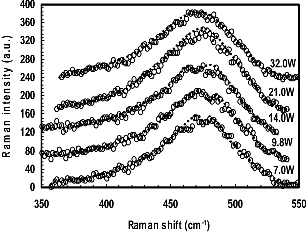
7.0W 9.8W 14.0W 21.0W 32.0W
0 40 80 120 160 200 240 280 320 360 400
350 400 450 500 550
Raman shift (cm-1)
R
a
m
a
n
in
te
n
s
it
y
(
a
.u
.)
flow-rates. The Raman spectra for all films showed broad peaks near at 480 cm-1 indicating amorphous phase in the film. The Raman spectra for the films prepared at silane flow-rate of 40, 30 and 20 sccm showed a sharp protruding peak at 495 cm-1 emerging from the broad amorphous peak. The Raman peak at 495 cm-1 corresponds to the scatterings from grains boundaries [9]. This indicates that the films consists of nano-sized crystallites embedded in a dominant amorphous matrix and the grain boundary which separates the nanocrystallites from the amorphous structure is more dominant than the nano-sized crystallites.
The Raman spectra for the films prepared at different discharge power is shown in Figure. 6. The peak at 495 cm-1 is observed as a small protrusion in the Raman spectra of the films prepared at low discharge power of 7 to 14 W. As in the above case, this indicates that films prepared at high discharge power are purely amorphous and nano-crystallites are formed only in the films prepared at low discharge power. Referring to figure 4, these films are also more ordered with low R parameter values. Therefore formation of nano-crystallites in the film structure results in a more ordered film structure. We believe that these nano-crystallites are formed in the ordered layers formed during the OFF-time of the discharge and at the initial onset of the discharge and these layers are ultra-thin and are less that 1nm thick. During the OFF-time, H etching effects dominates if sufficient H atoms are present. This removes weak Si-Si bonds and creates growth sites for a more ordered film structure in the presence of SiH3 radicals at the onset of the discharge.
CONCLUSIONS
The infrared and Raman spectroscopy of pulsed PECVD a-Si:H films prepared using our home-built system have been studied. The effects of silane flow-rates and discharge powers on the infrared and Raman spectra of these films have been analyzed. The films prepared at higher SiH4 flow-rates and low discharge powers have higher H content and indicate a more ordered film structure. The more ordered film structure in these films is due to the presence of crystallites in these films. We believe that the nano-crystallites are formed in ultra-thin layers formed during the OFF-time of the discharge and the initial onset of the discharge which are separated from each other by an amorphous layer formed during the ON-time of the discharge. H etching effects and SiH3 being the dominant deposition precursors play an important role in the formation of these multi-layers of highly-ordered and amorphous structure.
ACKNOWLEDGEMENT
REFERENCES
[1] Mukherjee, C., Anandan, C., Seth, T., Dixit, P.N. and Bhattacharyya, P., (2003); Thin Solid Films, 423, 18.
[2] Scott Morrison, Jianping Xi and Arun Madan, (1998); Mater. Res. Soc. Symp.,
507, 559.
[3] Kimura, H., Murakami, H., Nakahigashi, T., Ohtani, S., Tabata, T., Hayashi, T., Kobayashi, M., Mitsuda, Y., Kuwahara, H. and Doi, A., (1994); J. Appl. Phys., 33, 4398.
[4] Hadjadj, A., Beorchia, A., Roca i Cabarrocas, P. and Boufendi, L., (2002); Thin Solid Films, 139, 403-404.
[5] Boufendi, L. and Bouchoule, A., (1994); Plasma Sources Sci. Technol., 3,
262.
[6] Ruther, R. and Livingstone, J., (1994); Thin Solid Films, 251, 30. [7] Bhattacharya, E. and Mahan, A.H., (1988); Appl. Phys. Lett., 52, 1587.
[8] Zhang, S., Liao, X., Xu, Y., Martins, R., Fortunato, E. and Kong, G., (2004); J. Non-Cryts. Solids, 188, 338-340.