http://dx.doi.org/10.4236/cs.2015.63006
How to cite this paper: Singh, G., Prasad, D. and Bhaskar, D.R. (2015) Single VDVTA-Based Voltage-Mode Biquad Filter. Cir-cuits and Systems, 6, 55-59. http://dx.doi.org/10.4236/cs.2015.63006
Single VDVTA-Based Voltage-Mode Biquad
Filter
Ghanshyam Singh1, Dinesh Prasad2*, D. R. Bhaskar2
1Department of Electronics and Communication Engineering, HMRITM, Hamidpur, Delhi, India
2Department of Electronics and Communication Engineering, Faculty of Engineering and Technology, Jamia Millia Islamia, New Delhi, India
Email: [email protected], *[email protected], [email protected]
Received 19 February 2015; accepted 19 March 2015; published 20 March 2015
Copyright © 2015 by authors and Scientific Research Publishing Inc.
This work is licensed under the Creative Commons Attribution International License (CC BY). http://creativecommons.org/licenses/by/4.0/
Abstract
In this paper, an application of voltage differencing voltage transconductance amplifier (VDVTA) in the realization of voltage-mode (VM) multi-input single output (MISO) type biquad is presented. The proposed topology uses one VDVTA as an active element, two capacitors and a grounded re-sistor. The configuration realizes low pass (LP), high pass (HP), band pass (BP) and notch (BR) fil-ters without the requirement of any matching condition. The natural frequency (ω0) and band-
width (BW) are independently controllable. The proposed circuit offers low active and passive sensitivities of ω0. The operation of the proposed circuit has been verified through SPICE
simula-tion with TSMC CMOS 0.18 μm process parameters.
Keywords
Voltage Differencing Voltage Transconductance Amplifier, Analog Filter, LP, HP, BP, BR, Voltage Mode
1. Introduction
A number of VM MISO biquads utilizing different active elements have been proposed by the various research-ers employing single active device [1]-[11]. MISO-type biquads are especially vresearch-ersatile because the same to-pology can be utilized through proper selection of input signal(s) to realize different filter functions. Such filters may be used in the implementation of touch tone telephone systems, FM stereo demodulators, phase locked loop etc. [12]. A number of new active elements have been presented in [13]. Recently Shaktour in [14] has used VDVTA in the formation of first order all pass (AP) filter. In this communication, we propose another
tion using single VDVTA for the realization of MISO-type biquad using three inputs and one output with two capacitors and one grounded resistor. The proposed circuit realizes four basic filter functions, namely LP, HP, BP and BR. In the case of LP filter, the structure enjoys an extra advantage of having both the capacitors grounded as preferred for integration point of view [15]. The circuit offers the advantage of independent control
of ω0 and 0
0 Q
ω
. SPICE simulation results using TSMC CMOS 0.18 μm process and ±0.9 V DC power supply
voltages verify the theoretical prediction.
2. The Proposed Circuit Topology
The block diagram of the VDVTA is shown in Figure 1, where VP, VN and V are input terminals and Z, X+ and X− are output terminals. All terminals of VDVTA exhibit high impedance values [14]. The VDVTA can be characterised by the following terminal equations:
(
)
(
)
(
)
1 P N , 2 and 2 .
Z m V V X m Z V X m Z V
I =g V −V I + =g V −V I + = −g V −V (1)
The circuit analysis of Figure 2 yields the following output equation in terms of input signals:
2 1 2
2
1 2
2
3 2 1
2 1 2
0
2 1
2 1 2
. 1
m m m
m
m m
g g g
s V s V V
C C C
V
g
g g R
s s
C C C
+ +
=
+
+ +
(2)
Through proper selection of input signal(s) from Equation (2), Figure 2 realizes the following filter functions: 1) LPF; if V1=Vin and V2 =V3 =0 i.e.,
( )
( )
( )
( )
1 2
0 1 2
1 in
. m m g g
V s C C
T s
V s = = D s (3)
V
X Z
X
P
VDVTA VN
+
-IX+
IX
-IZ
VZ VP
V
VN
V
[image:2.595.238.384.293.376.2]VV V
Figure 1.The symbolic notation of VDTA.
R1
C1
V Z X
X
P
VDVTA
VN +
-C2 V0
V3
V2
V1
V
[image:2.595.215.414.426.704.2]2) BPF; if V2=Vin and V1=V3=0 i.e.,
( )
( )
( )
( )
2 2 0 2 in . m g s C V s T sV s D s
= = (4)
3) HPF; if V3 =Vin and V1=V2 =0 i.e.,
( )
0( )
( )
( )
23
in
.
V s S
T s
V s D s
= = (5)
4) BRF; if V1=V3=Vin and V2=0 i.e.,
( )
( )
( )
( )
1 2 2 1 2 0 4 in m m g g S C C V s T sV s D s
+
= = (6)
from Equations (3)-(6), it is clear that there is no requirement of any matching condition. Where
( )
21 2
2 1
2 1 2
1 . m m m g g g R
D s s s
C C C
+ = + +
The natural frequency ω0,
0 0 BW Q ω =
and quality factor Q0 are given by:
1 2 0 1 2 m m g g C C
ω = (7)
2 1 2 1 BW m g R C + = (8) 1 2 2 2 0 2 1 1 . 1 m m m g g C Q C g R = + (9)
The sensitivities of ω0 with respect to passive components are found to be:
0 0 0 0
1 2
1 2
1 1 1 1
, , ,
2 2 2 2
m m
g g C C
Sω = Sω = Sω = − Sω = −
which are all low.
3. Simulation Results
[image:3.595.89.550.108.598.2]M4
M1
M8
M5 M6
M7
M3
M2
Vn
Vp
Ib2
Ib1
Z
Ib4
Ib3
Vss
VDD
V
X- X+
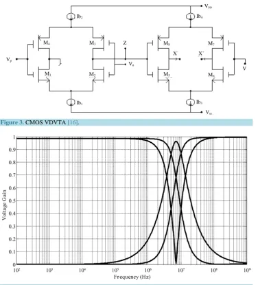
[image:4.595.129.506.81.497.2]Figure 3.CMOS VDVTA [16].
[image:4.595.128.498.543.723.2]Figure 4.Frequency response.
Table 1. Comparison of proposed biquad with other available MISO-type VM-biquads using a single active device.
Reference Number of resistors used
Number. of capacitors used
Whether all five filter functions are realized?
Requirement of matching conditions/constraints
[1] 3/2 2/3 No No
[2] 5 2 No Yes
[3] 1 2 Yes No
[4] 2 2 Yes Yes
[5] 3 2 Yes Yes
[6] 4 4 Yes Yes
[7] 2 2 Yes Yes
[8] 2 2 Yes Yes
[9] 2 2 Yes Yes
[10] 2 2 No No
[11] 3 2 No Yes
4. Conclusion
In this paper, an application of VDVTA is proposed in the form of VM-MISO-type biquad using three passive components. The proposed filter can realize the second-order LP, BP, HP and BR responses without changing the circuit topology and without any matching constraint(s). The LP filter response enjoys an additional advan-tage of having both the capacitors grounded as preferred for integration point of view [15]. The circuit offers low active and passive sensitivities. The SPICE simulation results using TSMC CMOS 0.18 μm process confirm the workability of the proposed structure.
References
[1] Hou, C.L., Huang, C.C., Lan, Y.S., Shaw, J.J. and Chang, C.M. (1999) Current-Mode and Voltage-Mode Universal Biquads Using a Single Current-Feedback Amplifier. International Journal of Electronics, 86, 929-932.
http://dx.doi.org/10.1080/002072199132923
[2] Sharma, R.K. and Senani, R. (2003) Multifunction CM/VM Biquads Realized with a Single CFOA and Grounded Ca-pacitors. AEU: International Journal of Electronics and Communications, 57, 301-308.
http://dx.doi.org/10.1078/1434-8411-54100176
[3] Prasad, D., Bhaskar, D.R. and Srivastava, M. (2013) Universal Voltage-Mode Biquad Filter Using a VDTA. Indian Journal of Pure and Applied Physics, 51, 864-868.
[4] Sagbas, M. and Koksal, M. (2007) Voltage-Mode Three-Input Single-Output Multifunction Filters Employing Mini-mum Number of Components. FREQUENZ: Journal of RF-Engineering and Telecommunications (Germany), 61, 87-
93. http://dx.doi.org/10.1515/FREQ.2007.61.3-4.87
[5] Prasad, D., Bhaskar, D.R. and Singh, A.K. (2009) Multi-Function Biquad Using Single Current Differencing Trans-conductance Amplifier. Analog Integrated Circuits and Signal Processing (USA), 61, 309-313.
http://dx.doi.org/10.1007/s10470-009-9310-1
[6] Keskin, A.U. (2006) Multi-Function Biquad Using Single CDBA. Electrical Engineering, 88, 353-356.
http://dx.doi.org/10.1007/s00202-004-0289-4
[7] Herencsar, N., Koton, J., Vrba, K. and Lattenberg, I. (2010) New Voltage-Mode Universal Filter and Sinusoidal Oscil-lator Using Only Single DBTA. International Journal of Electronics, 97, 365-369.
http://dx.doi.org/10.1080/00207210903325229
[8] Tangsrirat, W. and Channumsin, O. (2011) Voltage-Mode Multifunctional Biquadratic Filters Using Single DVCC and Minimum Number of Passive Elements. Indian Journal of Pure and Applied Physics, 49, 703-707.
[9] Kumar, P. and Pal, K. (2008) Universal Biquadratic Filter Using a Single Current Conveyor. Journal of Active and Passive Electronic Devices, 3, 7-16.
[10] Shah, N.A., Rather, M.F. and Iqbal, S.Z. (2005) A Novel Voltage-Mode Universal Filter Using a Single CFA. Journal of Active and Passive Electronic Devices, 1, 183-188.
[11] Chen, H.P. (2010) Single CCII-Based Voltage-Mode Universal Filter. Analog Integrated Circuits and Signal Process-ing (USA), 62, 259-262. http://dx.doi.org/10.1007/s10470-009-9345-3
[12] Chang, C.M. and Chen, H.P. (2005) Single FDCCII-Based Tunable Universal Voltage-Mode Filter. Circuits, Systems and Signal Processing, 24, 221-227. http://dx.doi.org/10.1007/s00034-004-0422-7
[13] Biolek, D., Senani, R., Biolkova, V. and Kolka, Z. (2008) Active Elements for Analog Signal Processing; Classifica-tion, Review and New Proposals. Radioengineering, 17, 15-32.
[14] Shaktour, I.M. (2011) Unconventional Circuit Elements for Ladder Filter Design. Ph.D. Thesis.
https://www.vutbr.cz/www_base/zav_prace_soubor_verejne.php?file_id=35975
[15] Bhushan, B. and Newcomb, R.W. (1967) Grounding of Capacitors in Integrated Circuits. Electronics Letters, 3, 148- 149. http://dx.doi.org/10.1049/el:19670114