© 2018, IRJET | Impact Factor value: 6.171 | ISO 9001:2008 Certified Journal | Page 2640
Design of Switched Filter Bank using Chebyshev Low pass Filter
Response for Harmonic Rejection Filter Design
Ann Alex
1, Sanju Sebastian
2, Niju Abraham
31
M.Tech Student, Department of Electronics and Communication Engineering, St. Joseph’s College of Engineering
and Technology, Kerala, India,
2
Assistant Professor, Department of Electronics and Communication Engineering, St. Joseph’s College of
Engineering and Technology, Kerala, India,
3
Assistant General Manager, Department of Aerospace and Defense, Cyient Limited, Karnataka, India.
---***---Abstract
- Harmonic is a serious problem faced by the poweramplifier in its working. These are introduced into the power amplifier due to the nonlinearities of the active element such as the transistor in the power amplifier. As a result, the power quality and safe operation become inferior. Therefore the mitigation of harmonics and improvement in the power quality are essential under these circumstances. This paper presents the design of a switched filter bank for using Chebyshev low pass filter response for the design of Harmonic Rejection Filter. Advanced Design System is used for simulation purpose. The obtained results show that each filter bank rejects its harmonic frequencies successfully with a return loss >16 dB.
Key Words:
Harmonics, Switched Filter Bank,
Chebyshev Low pass Filter, Harmonic Rejection Filter, Advanced Design System, Return Loss.
1. INTRODUCTION
During 20th century, evolutions in radios, communications and radars increased the demand for electromagnetic spectrum. Since the demand for Radio Frequency Spectrum has increased and become commercialized for different applications like mobile communications, television and radio communications, a clean radiation spectrum is a must for each radio transmissions. This has to be ensured by the RF front end of each radio transmitters. The RF front end section includes power amplifiers and they introduce harmonics to the signal and these harmonics are a multiple of operating frequencies and causes serious impurities in the spectrum. A demand for higher data rate implies a demand for higher bandwidth for the radio spectrum. This makes the elimination of the harmonics tougher for the RF front-end modules.
This motivates the need for an in-house Harmonic Rejection Filter technology in India. The Harmonic Rejection Filter is basically a low pass filter which passes the fundamental frequency and attenuates the higher harmonic frequencies. Passive filters have low cost, simple design and high reliability than active filters. Chebyshev filters have better rate of attenuation beyond passband than Butterworth filters. This paper presents the design of a switched filter bank using Chebyshev low pass filter for the design of Harmonic Rejection Filter.
2. METHODOLOGY
Chebyshev filters or equiripple filters have a steeper roll-off and more passband ripple than Butterworth filters. The analytic form of the squared magnitude function is defined by
where ε is the ripple factor, Tn(x) is the Chebyshev polynomial of degree n and ωp is the passband edge frequency. Closed form expressions for the Chebyshev polynomial are given by
be defined by a recursion formula:
where T0(x)=1 and T1(x)=x. The order of the Chebyshev
filter is given by the equation:
where As is the minimum stopband attenuation in dB, Ap in the maximum passband ripple in dB, ε =(100.1Ap −1)1/2 is the ripple factor, A = (100.05As)1/2 is the user-defined stopband attenuation parameter, ωs is the stopband edge frequency in rad/sec and ωp is the passband edge frequency in rad/sec.
© 2018, IRJET | Impact Factor value: 6.171 | ISO 9001:2008 Certified Journal | Page 2641 The Chebyshev low pass filter prototype element values are
given by the following equations:
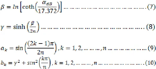
g1and gk are the capacitor or inductor element values. The coefficients β, γ, ak and bk can be calculated from the following equations:
where αdB is the passband ripple in dB. The number 17.372 is rounded from the exact value 40/ln (10). The low pass filter element values are given by
where Zo is the characteristic impedance in ohm and ωc=2πfcis the angular frequency in rad/sec, fc is the cut-off frequency of the filter in Hz.
3. RESULT AND DISCUSSIONS
In this paper, 30-512 MHz frequency range is assumed to be divided into six filter banks and each filter bank has been simulated separately in the Advanced Design System (ADS) environment.
3.1 Filter Bank 1: 30-50 MHz
Here, 30-50 MHz filter bank operates on 30-50 MHz band which passes up to 50 MHz with a passband ripple of -0.1 dB and start offering rejection from 50 MHz (cut-off frequency) with a stopband frequency of 60 MHz which offers a rejection around -24 dB. Table-1 shows the circuit parameters used in this simulation.
Pass band Frequency, ωp 30-50 MHz Stopband Frequency, ωs 60 MHz Pass band Ripple -0.1 dB Stopband Rejection -24 dB
Filter Order, n 9
Table-1: Circuit Parameters
Table-2 shows the inductor and capacitor values used in this schematic design.
Inductor L1 = L4 L2 = L3 L5 Values 229.60 nH 257.31 nH - Capacitor C1 = C5 C2 = C4 C3
[image:2.595.35.287.309.420.2]Values 76.119 pF 135.89 pF 140.40 pF
[image:2.595.309.565.368.505.2]Table-2: Inductor and capacitor values
Fig-1 shows the schematic design for ADS simulation.
[image:2.595.328.542.556.708.2]Fig-1: Schematic Design
Fig-2 shows the ADS simulation results and observations.
© 2018, IRJET | Impact Factor value: 6.171 | ISO 9001:2008 Certified Journal | Page 2642 Here the color cyan represents the Chebyshev filter response
and the color magenta represents the Low pass filter response. From the plot, it is clear that the signal is passed up to the cut-off frequency, 50 MHz and beyond the cut-off frequency, known as harmonic frequency, 60 MHz, the signal is rejected with a stopband rejection of -24 dB. From the plots, it is clear that for a filter bank 1 with passband ripple (-0.1 dB) and stopband rejection (-24 dB) will have a return loss, RL= -16.424 dB.
3.2 Filter Bank 2: 50-85 MHz
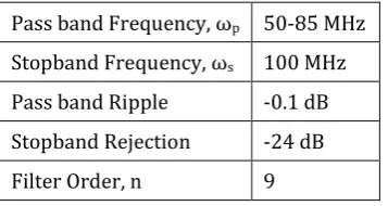
Here, 50-85 MHz filter bank operates on 50-85 MHz band which passes up to 85 MHz with a passband ripple of -0.1 dB and start offering rejection from 85 MHz (cut-off frequency) with a stopband frequency of 100 MHz which offers a rejection around -24 dB. Table-3 shows the circuit parameters used in this simulation.
Pass band Frequency, ωp 50-85 MHz Stopband Frequency, ωs 100 MHz Pass band Ripple -0.1 dB Stopband Rejection -24 dB
[image:3.595.332.538.102.249.2]Filter Order, n 9
Table-3: Circuit Parameters
Table-4 shows the inductor and capacitor values used in this schematic design.
Inductor L1 = L4 L2 = L3 L5 Values 135.06 nH 151.36 nH - Capacitor C1 = C5 C2 = C4 C3
Values 44.776 pF 79.935 pF 82.587 pF
[image:3.595.74.253.298.393.2]Table-4: Inductor and capacitor values
Fig-3 shows the schematic design for ADS simulation.
Fig-3: Schematic Design
Fig-4 shows the ADS simulation results and observations.
Fig-4: Simulation result
Here the color cyan represents the Chebyshev filter response and the color magenta represents the Low pass filter response. From the plot, it is clear that the signal is passed up to the cut-off frequency, 85 MHz and beyond the cut-off frequency, known as harmonic frequency, 100 MHz, the signal is rejected with a stopband rejection of -24 dB. From the plots, it is clear that for a filter bank 2 with passband ripple (-0.1 dB) and stopband rejection (-24 dB) will have a return loss, RL= -16.426 dB.
3.3 Filter Bank 3: 85-142 MHz
Here, 85-142 MHz filter bank operates on 85-142 MHz band which passes up to 142 MHz with a passband ripple of -0.1 dB and start offering rejection from 142 MHz (cut-off frequency) with a stopband frequency of 170 MHz which offers a rejection around -24 dB. Table-5 shows the circuit parameters used in this simulation
Pass band Frequency, ωp 85-142 MHz Stopband Frequency, ωs 170 MHz Pass band Ripple -0.1 dB Stopband Rejection -24 dB
[image:3.595.343.525.496.597.2]Filter Order, n 9
Table-5: Circuit Parameters
Table-6 shows the inductor and capacitor values used in this schematic design.
Inductor L1 = L4 L2 = L3 L5 Values 80.844 nH 90.602 nH - Capacitor C1 = C5 C2 = C4 C3
Values 26.802 pF 47.848 pF 49.436 pF
[image:3.595.37.288.585.715.2]© 2018, IRJET | Impact Factor value: 6.171 | ISO 9001:2008 Certified Journal | Page 2643 Fig-5 shows the schematic design for ADS simulation.
[image:4.595.324.545.113.191.2]Fig-5: Schematic Design
Fig-6 shows the ADS simulation results and observations.
Fig-6: Simulation result
Here the color cyan represents the Chebyshev filter response and the color magenta represents the Low pass filter response. From the plot, it is clear that the signal is passed up to the cut-off frequency, 142 MHz and beyond the cut-off frequency, known as harmonic frequency, 170 MHz, the signal is rejected with a stopband rejection of -24 dB. From the plots, it is clear that for a filter bank 2 with passband ripple (-0.1 dB) and stopband rejection (-24 dB) will have a return loss, RL= -16.428 dB.
3.4 Filter Bank 4: 142-236 MHz
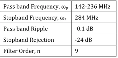
Here, 142-236 MHz filter bank operates on 142-236 MHz band which passes up to 236 MHz with a passband ripple of -0.1 dB and start offering rejection from 236 MHz (cut-off frequency) with a stopband frequency of 284 MHz which offers a rejection around -24 dB. Table-7 shows the circuit parameters used in this simulation.
Pass band Frequency, ωp 142-236 MHz Stopband Frequency, ωs 284 MHz Pass band Ripple -0.1 dB Stopband Rejection -24 dB
Filter Order, n 9
Table-7: Circuit Parameters
Table-8 shows the inductor and capacitor values used in this schematic design.
Inductor L1 = L4 L2 = L3 L5 Values 48.644 nH 54.515 nH - Capacitor C1 = C5 C2 = C4 C3
Values 16.127 pF 28.790 pF 29.745 pF
Table-8: Inductor and capacitor values
[image:4.595.308.560.243.374.2]Fig-7 shows the schematic design for ADS simulation.
[image:4.595.62.263.260.396.2]Fig-7: Schematic Design
[image:4.595.332.533.428.603.2]Fig-8 shows the ADS simulation results and observations.
Fig-8: Simulation result
[image:4.595.67.259.644.739.2]© 2018, IRJET | Impact Factor value: 6.171 | ISO 9001:2008 Certified Journal | Page 2644 3.5 Filter Bank 5: 236-394 MHz
Here, 236-394 MHz filter bank operates on 236-394 MHz band which passes up to 394 MHz with a passband ripple of -0.1 dB and start offering rejection from 394 MHz (cut-off frequency) with a stopband frequency of 472 MHz which offers a rejection around -24 dB. Table-9 shows the circuit parameters used in this simulation.
Pass band Frequency, ωp 236-394 MHz Stopband Frequency, ωs 472 MHz Pass band Ripple -0.1 dB Stopband Rejection -24 dB
[image:5.595.64.263.182.272.2]Filter Order, n 9
[image:5.595.341.529.298.393.2]Table-9: Circuit Parameters
Table-10 shows the inductor and capacitor values used in this schematic design.
Inductor L1 = L4 L2 = L3 L5 Values 29.137 nH 32.654 nH - Capacitor C1 = C5 C2 = C4 C3 Values 9.6597 pF 17.245 pF 17.817 pF
[image:5.595.352.517.457.532.2]Table-10: Inductor and capacitor values
[image:5.595.44.279.459.562.2]Fig-9 shows the schematic design for ADS simulation.
Fig-9: Schematic Design
Fig-10 shows the ADS simulation results and observations.
Fig-10: Simulation result
Here the color cyan represents the Chebyshev filter response and the color magenta represents the Low pass filter response. From the plot, it is clear that the signal is passed up to the cut-off frequency, 394 MHz and beyond the cut-off frequency, known as harmonic frequency, 472 MHz, the signal is rejected with a stopband rejection of -24 dB. From the plots, it is clear that for a filter bank 2 with passband ripple (-0.1 dB) and stopband rejection (-24 dB) will have a return loss, RL= -16.421 dB.
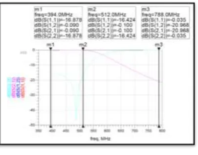
3.6 Filter Bank 6: 394-512 MHz
Here, 394-512 MHz filter bank operates on 394-512 MHz band which passes up to 512 MHz with a passband ripple of -0.1 dB and start offering rejection from 512 MHz (cut-off frequency) with a stopband frequency of 788 MHz which offers a rejection around -24 dB. Table-11 shows the circuit parameters used in this simulation.
Pass band Frequency, ωp 394-512 MHz Stopband Frequency, ωs 788 MHz Pass band Ripple -0.1 dB Stopband Rejection -24 dB
Filter Order, n 5
Table-11: Circuit Parameters
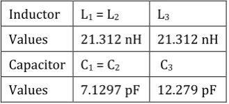
Table-12 shows the inductor and capacitor values used in this schematic design.
Inductor L1 = L2 L3
Values 21.312 nH 21.312 nH Capacitor C1 = C2 C3 Values 7.1297 pF 12.279 pF
Table-12: Inductor and capacitor values
Fig-11 shows the schematic design for ADS simulation.
[image:5.595.313.554.585.719.2]© 2018, IRJET | Impact Factor value: 6.171 | ISO 9001:2008 Certified Journal | Page 2645 Fig-12 shows the ADS simulation results and observations.
Fig-12: Simulation result
Here the color cyan represents the Chebyshev filter response and the color magenta represents the Low pass filter response. From the plot, it is clear that the signal is passed up to the cut-off frequency, 512 MHz and beyond the cut-off frequency, known as harmonic frequency, 788 MHz, the signal is rejected with a stopband rejection of -24 dB. From the plots, it is clear that for a filter bank 2 with passband ripple (-0.1 dB) and stopband rejection (-24 dB) will have a return loss, RL= -16.424 dB.
4. CONCLUSION
In this paper, the design of a 6 channel switched filter bank for 30-512 MHz frequency range using Chebyshev low pass filter response for the design of Harmonic Rejection Filter was presented. The proposed filter bank improves the power quality by rejecting the harmonic frequencies with a return loss >16 dB. The obtained results meet the IEEE 519 recommended harmonic standards.
ACKNOWLEDGEMENT
The authors would like to acknowledge Department of Aerospace and Defense, Cyient Limited, Bangalore, for providing the lab facilities to complete this research work.
REFERENCES
[1] Z. H. Zhao, P. H. Li, K. L. Cheng, W.-Q. Cao and K. H. Chen,
High power VHF Frequency Hopping Filters with High Suppression of Second Harmonics, Prog. Electromag. Research Lett., vol. 20, 119-128
[2] David J. DeFatta, Joseph G. Lucas and William S.
Hodgkiss, Digital Signal Processing: A System Design Approach, Ed. Wiley, 1988
[3] John L Stensby (2011), Chebyshev filters [Online].
Available: www.ece.uah.edu/courses /Chebyshev.pdf
[4] Giovanni Bianchi and Roberto Sorrentino, Lumped
Passive Filters in Electronic Filter Simulation Design, Ed. McGraw Hill, 2007, 31-43
[5] Jose Maria Giron Sierra, Digital Signal Processing with
Matlab Examples, Volume 1: Signals and Data, Filtering, Non-stationary Signals, Modulation, Ed. Springer, 2016
[6] R. E. Collin, Foundations for Microwave Engineering,
2nd Ed., Ed. Wiley IEEE Press, 2000.
[7] G. Bianchi, Electronic Filter Simulation & Design, 1st Ed.,
Ed. McGraw-Hill, 2007.
[8] Annapurna Das and Sisir K Das, Microwave Engineering,