University of Huddersfield Repository
Charitopoulos, Romanos
Implementation & Performance Investigation of Dicode PPM over Dispersive Optical Channels
Original Citation
Charitopoulos, Romanos (2009) Implementation & Performance Investigation of Dicode PPM over Dispersive Optical Channels. Doctoral thesis, University of Huddersfield.
This version is available at http://eprints.hud.ac.uk/id/eprint/7241/
The University Repository is a digital collection of the research output of the University, available on Open Access. Copyright and Moral Rights for the items on this site are retained by the individual author and/or other copyright owners. Users may access full items free of charge; copies of full text items generally can be reproduced, displayed or performed and given to third parties in any format or medium for personal research or study, educational or notforprofit purposes without prior permission or charge, provided:
• The authors, title and full bibliographic details is credited in any copy; • A hyperlink and/or URL is included for the original metadata page; and • The content is not changed in any way.
For more information, including our policy and submission procedure, please contact the Repository Team at: [email protected].
Implementation & Performance Investigation of
Dicode PPM
over Dispersive Optical Channels
Romanos Athanasiou Charitopoulos
A thesis submitted to the University of Huddersfield
in partial fulfilment of the requirements for
the degree of Doctor of Philosophy
Abstract
This work is concerned with the development and investigation of a Dicode PPM (DiPPM) system.
A DiPPM coder was developed to code any input PCM signal into DiPPM format. A further investigation took place on the DiPPM spectrum and associated output. Software simulation and mathematical analysis of this PPM code was considered and comparison with previous theoretical results presented. Results show that DiPPM is an advantageous PPM code for optic communication; DiPPM spectrum is not concentrated near to DC and it is possible to extract the DiPPM framerate component directly from the pulse stream. A timing extraction circuit that recovers the clock from a DiPPM sequence and synchronises the slots within the frames, was constructed successfully. This enabled transmission through fibre optics and Free Space Optics (FSO). The technique used for the timing extraction circuit of the DiPPM scheme gives an advantage over many of the PPM formats.
An optical transmitter/receiver system was developed and the DiPPM scheme was investigated through optical channels. Results show that the DiPPM sequence transferred through the optic system was not changed and the clock had been recovered. A DiPPM decoder was constructed and the received DiPPM signal returned to its original PCM form without errors.
Both DiPPM coder and decoder were developed in VHDL and measurements were taken. The timing extraction was programmed in VHDLAMS with the use of digital, analogue and mathematical equations.
Acknowledgements
The author would like to thank lecturers and staff of Huddersfield University for their help throughout this project, in particular:
My academic supervisor and mentor Dr. M.J.N. Sibley for his advice, guidance and encouragement over the duration of the research project.
Thanks must also go to my academic supervisor Dr. P.J. Mather for his advice and assistance in the coding of my work into software program.
I also wish to acknowledge Mr. Jack Briggs and Mr. David Bray for their support on technical matters and Mr. D.C. Andrews and Mr. Anver Dadhiwala for their help with the software.
Glossary of Symbols
Symbol Definition
A Amplitude
BdW Bandwidth of the preamplifier
C Capacitor.
c
C Collector emitter capacitance
d
C The emitterbase capacitance
f
C Capacitance at the feedback resistor Cn The amplitude spectrum
DiPPMprbs DiPPM PRBS sequence
y x
Error , Number of PCM errors the event generates.
f Frequency
fs Phase shift )
(t
h Power Spectral Density (PSD) of a PCM sequence.
) ( t DiPPM
h Power Spectral Density (PSD) of a DiPPM sequence.
0
K The VCO conversation gain.
2 0
n The mean square noise of the receiver.
( )
2 0 t
n The mean square receiver output noise.
e
P Equivalent PCM error probability (DiPPMISI).
eb
P The average binary error probability
efN
er
P The PCM error probability for erasures.
erDiPPM
P The PCM error probability for erasure.
Ts efR
P - The equivalent PCM error probability.
f
P The probability of a false alarm error.
(
PfISI 1)
The following symbol of an Sslot.
(
PfISI 2)
The previous symbol of an Sslot.
R S fN
P ® / The probability of a false alarm in either the S or R slot of a blank
frame
r
P The probability of an erasure error at DiPPM without ISI
s
P The probability of a pulse appearing in the preceding slot (wrong slot).
t
P The probability of false alarm error in DiPPM.
y x
P , Probability of a particular error event occurring.
R Is the symbol for DiPPM RESET (01).
2
R Resistor.
1
Re set Independent pulse train.
2
Re set Independent pulse train.
S Is the symbol for DiPPM SET (10). 1
Set Independent pulse train. 2
Set Independent pulse train. T The clock period.
d
t The slope of the received pulse at the threshold crossing instant.
R
become small. (DiPPMISI)
R
T The time at which the autocorrelation function of the receiver filter has become small (DiPPM)
d
v The threshold voltage.
f
V The VCO control voltage from the Loop Filter. Vin The loop input voltage
) (
0 t d
v The ISI voltage at the decision time in the time slot under consideration. Vout The loop output voltage
pk
v The peak signal voltage at the output of the receiver for either an S or R pulse.
1 0ISI
v The probabilities of
(
PfISI 1)
.
2 0ISI
v The probabilities of
(
P fISI 2)
.
(
x y t)
V oS , , Shape of the SET pulse.
(
x y t)
V oR , , Shape of the RESET pulse.
W Window equation.
X(t) DiPPM signal when PCM signal starts with a positive pulse (logic 1) X(t) DiPPM signal when PCM signal starts with a negative pulse (logic 0)
z The damping factor
w The ratio of input frequency.
0
w The VCO output frequency.
Operator Notation
[]
å
. Sum of terms.
[ ]
*
. Complex conjugate
[ ]
.Absolute value
[] []
. * .Convolution.
[]
.
Contents
Abstract
2
Acknowledgements
3
Glossary of Symbols
4
Operator Notation
7
List of Tables
13
List of Figures
14
Chapter 1
INTRODUCTION 19
1.1 Aims and Objectives 22
1.2 Document Structure 24
Chapter 2
LITERATURE REVIEW 28
2.1 PPM and Optical Channels 30
2.2 Timing Extraction and Synchronisation 32
2.3 PPM and Error Corrections 34
2.4 Multiple PPM 36
2.5 Differential PPM 39
2.6 DHPIM, PIM, DPIM 41
2.7 Digital PPM 42
2.8 Dicode technique 45
Chapter 3
Dicode PPM 47
3.1 Dicode PPM (ISI guards) 48
3.1.1 DiPPM (ISI) Error Sources and Probabilities 49
3.1.2 DiPPM (ISI)PINFET Receiver 56
3.1.3 Dicode PPM through Optical Wireless Communication 59
3.2 Dicode PPM 59
3.2.1 DiPPM Error Sources and Probabilities 60
3.2.2 DiPPMPINFET Receiver 65
Volume I of II
Hardware
Chapter 4
Dicode PPM Hardware 70
4.1 DiPPM Coder 71
4.1.1 Implementation of DiPPM Coder 71
4.1.2 Measurements from the DiPPM Coder 73
4.2 DiPPM Decoder 77
4.2.1 Implementation of DiPPM Decoder 77
4.2.1.1DiPPM Coder Technical Information 78
4.2.2 Measurements and confirmation of DiPPM Decoder 79
4.2 Conclusion 81
Chapter 5
Dicode PPM Simulations 82
5.1 DiPPM Software Simulations 82
5.2 DiPPM Mathematical Representation 86
5.3 DiPPM Windowing Method 95
Chapter 6
Dicode PPM Timing Extraction 102
6.1 DiPPM Clock Recovery Process 104
Chapter 7
Complete Dicode PPM using optical components 111
7.1 Analysis of Optical Parts and Measurements 113
7.2 Measurements of the Optical Received DiPPM Sequence 118
Volume II of II
‘Software’
Chapter 8
VHDL: Dicode PPM Coder/Decoder & Clock Recovery 125
8.1 DiPPM Coder/Decoder Simulation Version 126
8.1.1 DiPPM Coder 126
8.1.2 DiPPM Decoder 127
8.2 DiPPM Coder/Decoder Upgraded Version 129
8.2.1 DiPPM Coder 129
8.2.2 DiPPM Decoder 131
8.3 DiPPM Coder/Decoder RealTime Measurements 132
8.4 VHDLAMS: DiPPM Timing Extraction 136
8.4.1 Buffer 136
8.4.2 Phase Detector 137
8.4.3 Loop Filter 141
8.4.4 VCO 144
8.4.5 Digitaliser 145
Chapter 9
MLSD for DiPPM 149
9.1 Type of Errors that Affect DiPPM 149
9.2 DiPPM MLSD Construction 155
9.3 DiPPM system with MLSD 164
Chapter 10
Thesis Overview 166
10.1 Discussion 166
10.2 Further Work 169
10.3 Conclusion 171
APPENDICES 173
Appendix1 173
Appendix2 229
Appendix3 233
Appendix4 270
REFERENCES
241Bibliography
253Author’s Publications
250List of Tables
2A Multiple PPM coding formats 38
2B Differential PPM coding format. 40
2C Differential PPM coding format 44
2D Dicode Technique coding format 46
3A DiPPM symbol alphabet. 50
3.B Transmitted and received sequences with a wrongslot error. 52 3.C Transmitted and received sequences with a wrongslot error. 60 9A DiPPM MLSD: Wrongslot error and detection method. 150 9B DiPPM MLSD: Detection of a DiPPM sequence in which an
List of Figures
2.1 Conversion of 3 bits of PCM to multiple PPM. 38 2.2 Conversion of 6 bits of PCM to 12 bits multiple PPM. 39 2.3 Conversion of 3 bits of PCM to differential PPM. 40 2.4 Conversion of 4 bits of PCM to digital PPM, to PIM and DHPIM. 42
2.5 Conversion of 4 bits of PCM to digital PPM. 44
2.6 Conversion of PCM to dicode technique. 46
3.1 Conversion of PCM to dicode technique and DiPPMISI. 49
3.2 Block diagram of DiPPM receiver. 57
3.3 Conversion of PCM data to dicode PPM. 59
3.4 DiPPMISI Spectral by[103]. 67
4.1 DiPPM coder’s circuit. 71
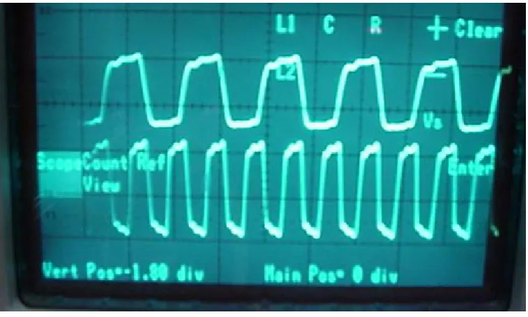
4.2 DiPPM coder’s waveforms. 72
4.3 DiPPM coder’s deterministic outcome and clock 73
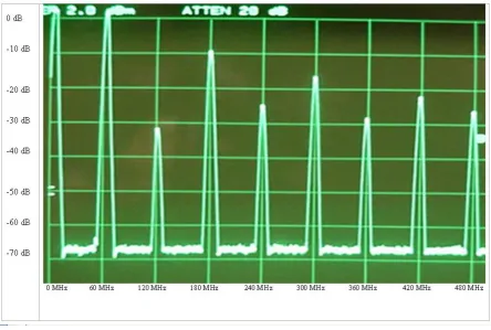
4.4 DiPPM PSD of deterministic sequence (hardware). 74
4.5 Uneven mark space on SET DiPPM pulse. 75
4.6 DiPPM coder’s PRBS outcome, clock sequence. 75
4.7 DiPPM PSD of PRBS sequence (hardware). 76
4.8 DiPPM decoder circuit. 77
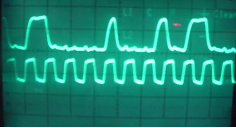
4.9 DiPPM decoder’s waveforms. 78
4.10 DiPPM decoder’s deterministic outcome and clock sequence. 79
4.11 DiPPM decoder’s output and DiPPM PRBS. 80
4.12a PCM deterministic input, PCM deterministic output. 80
5.1 Simulation’s plots of clock, deterministic PCM, deterministic DiPPM. 83 5.2 Simulation’s plots of clock, PRBS PCM, PRBS DiPPM. 84
5.3 PRBS PSD of DiPPM coder Simulation. 85
5.4 Deterministic PSD of DiPPM coder Simulation. 86
5.5 Relationship of deterministic PCM and DiPPM waveforms. 87
5.6 DiPPM deterministic sequence: X(t) and X(t). 88
5.7 Deterministic DiPPM PSD of X(t) and X(t). 89
5.8: Internal clock, pulse train 5.4a, pulse train 5., pulse train 5.5a,
pulse train 5.5b, PRBS DiPPM 5.6. 92
5.9 DiPPM PRBS of 60 bits. 93
5.10 Internal clock, PRBS DiPPM 5.6. 93
5.11 PRBS DiPPM PSD of equation 5.6. 94
5.12: Deterministic DiPPM spectrums from simulation and equation 3
with the use of window. 98
5.13 PRBS DiPPM spectrums from simulation and equation 6
with the use of window. 98
5.14 Random DiPPM spectrums from simulation with the use of window 99
5.15 DiPPM spectrum powers comparison 100
6.1 DiPPM timing extraction diagram. 103
6.2 Phase Detector Process. 104
6.3 Loop Filter transformed to Comparator. 105
6.4 DiPPM timing extraction waveforms. 106
6.8 Synchronous PRBS DiPPM, clock Timing Extraction’s outcomes. 109 6.9 Synchronous PRBS DiPPM spectrum as Timing Extraction’s outcomes 110 7.1: Complete DiPPM system with transmitter/receiver for optic communication 112
7.2a Optical Transmitting System. 112
7.2b Optical Receiving System. 113
7.3 ThresholdCrossing Detector 113
7.4 ThresholdCrossing Detector output, DiPPM input. 114
7.5: Si PIN preamplifier receiver. 115
7.6 Output of preamplifier, DiPPM from coder. 116
7.7 Output of thresholdcrossing detector, DiPPM from coder 117 7.8 Asynchronous Outcomes of Timing Extraction: PRBS DiPPM, Clock. 118 7.9 Synchronous Outcomes of Timing Extraction: PRBS DiPPM, Clock. 119 7.10 Optical DiPPM spectrum (synchronised DiPPMRecovered clock). 119
7.11 Optical DiPPM spectrum (simulated). 120
7.12 Optical DiPPM spectrum (from equation 5.5). 121
8.1 VHDL: Deterministic DiPPM coder simulation 126
8.2 VHDL: PRBS DiPPM coder simulation 127
8.3 DiPPM CoderDecoder 128
8.4 VHDL: Deterministic DiPPM decoder simulation 128
8.5 VHDL: PRBS DiPPM decoder simulation 129
8.6 VHDL: PRBS Upgraded DiPPM coder D flipflop included 130 8.7 VHDL: PRBS Upgraded DiPPM coder delay included 130
8.8 DiPPM upgraded versions of coderdecoder 131
8.9 VHDL: PRBS Upgraded DiPPM decoder delay included 132
8.11 VHDL: DiPPM coderdecoder in Quartus 133
8.12 VHDL: DiPPM coderdecoder outcomes 134
8.13 FPGA: PRBS DiPPM output sequence, PRBS PCM input sequence 134 8.14 FPGA: PRBS PCM output sequence, PRBS DiPPM input sequence. 135 8.15 FPGA: PRBS PCM output sequence, PRBS PCM input sequence. 135 8.16 PRBS DiPPM input, PRBS DiPPM output leaded to decoder,
PRBS DiPPM output leaded to PLL circuit. 137
8.17 Phase detector software process 138
8.18 Phase detector: Output sequence, Input Vin sequence, input clock VRef. 138
8.19 Phase detector (faulty) 140
8.20 Phase detector software process (faulty) 140
8.21 Phase detector (faulty) 141
8.22 Loop Filter (VHDLAMS) 142
8.23 Loop filter’s output when its input signal is PRBS DiPPM 143
8.24 PRBS DiPPM, VCO output 145
8.25 VCO output , Digitaliser output 146
8.26 DiPPM Vin, VCO clock, phase detector’s output. 147
8.27 DiPPM in, DiPPM out, clock recovered. 147
8.28 PCM in, clock recovered, PCM out. 148
9.1 First SET and RESET pulses of a DiPPM sequence 154
9.2 SET and RESET pulses of a DiPPM sequence (SNRNSRNS) 154
9.3 Erased SET immediately after RESET (RS) 155
9.4 DiPPM sequence without errors through MLSD 156
9.5 Wrong slot appears in DiPPM sequence (corrected). 156
9.7 Wrong slot S/S/S error corrected. 159
9.8: MLSD Flowchart. 160
9.9 Wrong slot S/S/S error corrected. 162
9.10 MLSD corrector corrections. 162
9.11 MLSD Flowchart with MLSD Corrector 163
9.12 Complete VHDL DiPPM system with MLSD 164
Chapter 1
INTRODUCTION
Optical communication is concerned with the transmission of information between two distant points using an optical carrier. The information can be transmitted in analogue or digital form. In analogue transmission, a source waveform has to be transmitted from the transmitter to the receiver with as little distortion as possible. However, in digital transmission the information is converted to binary symbols (bits). This information then modulates an optical carrier which is detected and decoded by the receiver into the original format. This digital information can be transmitted over the optical link on a bit bybit basis (binary encoding) or on a data word basis (block encoding).
technique, incorporated at the receiver is used to directly encode digital bits on the phase or frequency of the laser carrier. However, in all these systems only binary encoding was considered, in which bits are sent one at a time over the optical link. An alternative is the use of block encoding in which bits are transmitted in blocks.
Pulse Position Modulation (PPM) is a popular form of optical block encoding; M bits are coded by transmitting one pulse which is placed in one of 2 M
adjacent time slots to represent the data block. The M slots compose a PPM frame and the location of the pulse in the frame determines the data word. The system is compatible with direct detection receivers as it uses pulsed optics. The pulse width of the M bit is equal to the slot width. Therefore, the laser needs only to produce pulses at the frame rate which operates at the pulse repetition frequency.
The PPM decoder must then determine which of the M slots occurring during a time frame contains the optical pulse. In PPM, every symbol of the received signal has to be fully synchronised with the clock signal. This is achieved by the timing extraction system. Once the clock has been extracted and synchronised with the start edges of the received PPM signal, the PPM signal can be decoded to the original form by the PPM decoder. However, noise in the detection process can cause errors.
A number of PPM formats have been previously investigated; Multiple Pulse Position Modulation (MPPM) [112], Differential Pulse Position Modulation (DPPM) [1316] and many related modulation coding schemes such as Pulse Interval Modulation (PIM) [13, 1719], Digital Pulse Interval Modulation (DPIM) [2021] and Dual Header Pulse Interval Modulation (DHPIM) [2126]. Analysis has shown that while each code has many advantages when compared to Pulse Code Modulation (PCM), this occurs at the expense of bandwidth [2729]. This makes PPM systems attractive for use in glass fibre or directed line of sight networks where bandwidth is not at a premium. Unfortunately, glass optical fibre cable is expensive and unsuitable for everyday use such as networks. Conversely, Plastic Optical Fibre (POF) is inexpensive but has a low bandwidth making it unattractive for use with PPM schemes.
Previously, Digital PPM (DigPPM) had been proposed [2729] as the most appropriate coding scheme for optic communication when compared to the other PPM formats. However, digital PPM format means that while a sensitivity advantage is achieved over standard PCM, it does so at the expense of a large bandwidth expansion factor. This results in a final data rate that can be prohibitively high. This led to the investigation of various other PPM schemes of which, Dicode PPM (DiPPM) [27], was proposed by Sibley as a more advantageous format than DigPPM. DiPPM can be effectively implemented as it uses two slots to transmit one bit of PCM. Unlike DigPPM, DiPPM achieves greater sensitivity than PCM at a slot rate of twice the original PCM data rate
[2730].
optical DiPPM system (coder, timing extraction and decoder) is presented and analysed. The coder output is presented in both time and frequency domain, and experimental results are compared to mathematical representations and simulations. VHDL codes of the DiPPM system are presented, including a DiPPM error corrector.
1.1 Aims and Objectives
Investigations undertaken and intermediate objectives fulfilled during PhD research:
· To implement a system and practically verify some of the theoretical models. As no experimental construction of DiPPM coder/decoder had been presented at this time, a hardware DiPPM coder and decoder has to be implemented to further investigate the DiPPM format. Thus, it will be proved if DiPPM format can appear in real time (many PPM formats are remained in theoretical levels). The initial objective of the DiPPM coder/decoder is for it to be constructed using low cost components, giving an advantage over the majority of other PPM schemes.
· To confirm theoretical predictions with measurements.
must be analysed. Should PSD outcomes not agree with those of previous publications, further investigation must be carried out on DiPPM PSD and on differences that might appear.
· To confirm theoretical predictions with measurements (fibre optics).
The main focus of this thesis is to investigate the performance of DiPPM through optics. Thus, an optical system such as an optical transmitter/receiver, has to be constructed and the performance of DiPPM waveforms through Plastic Optical Fibre (POF) or freespace, determined. Since the DiPPM decoder will need a clock sequence to decode the DiPPM sequence into PCM format, a clock has to be recovered. Thus, the construction of a timing extraction system for DiPPM is required. Outputs of the DiPPM timing extraction system must be examined with concern for synchronisation (DiPPM, clock) and the PSD of the optical received DiPPM.
· Design and build a Dicode PPM system using FPGA.
It is expected that the discrete component based hardware for the DiPPM coder/decoder and timing extraction will be affected by external interference due to the high frequencies (240 MHz) used. Thus, the DiPPM coder/decoder and timing extraction will be synthesised onto an FPGA which will give reduced levels of delays, distortions, external and internal interferences, enabling the code to be fully evaluated.
· To investigate additional coding techniques such as MLSD (Maximum
The performance of the DiPPM scheme is to be investigated incorporating error correction. A Maximum Likelihood Sequence Detection (MLSD) will be developed for DiPPM, to correct or minimise errors that occur from a long distance optical communication or from faulty reception by the optical receiver DiPPM sequence. This MLSD will be programmed in VHDL, as it is expected that the circuit will be complex because of loops, long shift registers and parallel processes. It is considered that any MLSD construction with logic components will be adversely affected by asynchronisation. These may appear because of external interferences and from internal delays.
1.2 Document Structure
An introduction to the PPM format and possible errors is contained in the Chapter 1. It also contains a brief review of previous PPM formats and of the format that this thesis presents.
Chapter 2 presents the historical progress of PPM through time and optical systems. Mention is made of components, such as Timing Extraction and Error Corrector, which are essential in an optical PPM scheme. Finally, a brief description of the most frequently used PPM formats is presented.
Chapter 4 contains DiPPM coder and decoder circuit construction. The construction of DiPPM structures and output results are presented and discussed.
Chapter 5 confirms the results of chapter 4 through software simulation of the DiPPM coder and mathematical representations of DiPPM sequences. This chapter introduces the use of a window equation so that the simulated results match the experimental DiPPM system.
The Timing Extraction circuit of the DiPPM scheme and successful implementation are presented in Chapter 6. The optical system (transmitter/receiver) used for optical communication of the DiPPM system and measurements taken appear in Chapter 7.
The implementation of the DiPPM coder and decoder using FPGA is presented in Chapter 8; including DiPPM timing extraction.
Chapter 9 presents The Maximum Likelihood Sequence Detector (MLSD) error corrector coding technique of DiPPM format.
Chapter 10 concludes the work presented in this thesis, highlighting the original contribution of DiPPM and suggesting further work to be done on the DiPPM scheme.
1.3 Original work presented by the Author
· Hardware implementation of the DiPPM coder and decoder, developed by the author, shows that the DiPPM scheme can be achieved for real time operation. Outcomes agree with theory [2730].
· Software simulation of the Dicode PPM has been programmed. PCM deterministic and pseudorandom binary sequence inputs were coded successfully into DiPPM format. Outcomes such as spectrums and sequences are shown. Windowing equations are given and used in the simulation.[3132]
· Original practical measurements of the power spectral densities (deterministic pseudorandom binary sequence) are presented. These indicate that DiPPM is a suitable PPM coding format for optic wireless, fibre and free space communication. Results show that the DiPPM spectrum is not concentrated near DC frequencies [32].
· A timing extraction circuit for DiPPM which recovers and synchronises the clock from the DiPPM signal (DiPPMclock) is presented. The DiPPM spectrums, magnitudes and phase spectrums of optical DiPPM system are also presented.[33]
· VHDL codes have been developed for DiPPM coder and decoder.
· DiPPM Timing extraction has been coded on VHDLAMS.
Chapter 2
LITERATURE REVIEW
Many authors have discussed the performance of analogue PPM systems since Shannon’s
[34] paper, ‘Mathematical Theory of Communication’. This was followed one year later, in 1949, by a book coauthored with Weaver [35], describing a theoretical fundamental limit on channel efficiency and the modulation formats that could approach this limit..
Golay published a paper [36] the same year; a theoretical model based on a multichannel and threshold detection system as the first practical way of using digital PPM to attempt to achieve the Shannon limit. This digital PPM system was later named as QPPM and Golay is regarded as the founder of the QPPM systems.
changed Golay’s statement that QPPM word error probability can approach the theoretical limit of Shannon with as small error probability as desired. Unfortunately, after analysis was complete, Chang [40] found that Gruenberg’s results were not accurate. Later work showed that the word error probability of QPPM systems could not compare with the bit error probability of other modulation formats.
In 1973, Hubbard [41] presented the use of analogue PPM. This work analysed the effect of timing error and false alarm due to noise on the leading edge of the received pulse. Experiments on analogue PPM optical fibre were completed in 1975 by Holden [42]. Three years later, an investigation took place by Muoi and Hullett [43] on an analogue PPM system, for the minimisation of timing error due to noise on the pulse. A simple suboptimum receiver was proposed, which took into account interpulse interference whilst suffering only a small reduction in signal when compared to the optimum design. In 1978, a publication by Luciano and Pirani [44], presented an analysis of system behaviour in terms of coding efficiency, timing information and PSD of a combined Pulse Amplitude Modulation (PAM) and optical communication system. The main achievements of this system are an abundant timing frequency component, reduced low frequency component and longest interval without a signal level change being three times the symbol period. Compared with previous signalling formats, this system provides greater advantage for timing purposes.
was investigated by Gol’dsteyn and Frezinskiy [49] in the same year. Dolinar [50], with the use of Conditional Nulling Receivers, presented a receiver structure of digital PPM detection in 1982. This receiver has the ability to determine, whether to coherently combine a predetermined local oscillator field with the received optical field, prior to detection. A year later, Garrett considered the performance of optical fibre digital systems using PINFET optical receivers. In 1986, Pires and de Rocha [51] maintained that an APDFET receiver offers higher sensitivity than a PINFET in a digital PPM transmission over low level optical fibre and also greater sensitivity to that of PCM. At the same time, Mecherle [5253] analysed various coding and decoding conditions using optical digital PPM.
Numerous publications on the implementation and format of PPM have been presented. In order to provide the necessary background, so that the main focus of this thesis can be understood, a review of implementation and format is briefly presented.
2.1 PPM and Optical Channels
By the late 1970’s many authors [3444] were involved with the improvement of the digital PPM scheme. In the 1980’s digital PPM had evolved and been analysed for operation over optical fibre channels
receiver provides a sensitivity of 10 to 12 dB greater than that of PCM systems. This improvement gave an advantage to PPM format over optical fibre channel; for an attenuation of 0.2dB/km, it represents an increase of 50 to 60 km in regenerator spacing. Thus, for every 3 dB improvement in sensitivity, the number of customers being served in a multiuser environment can be doubled.
In 1988, Calvert [5658], using a theoretical model based on a modified Garrett analysis, completed digital PPM optical fibre experiments for the first time. He coded 7 PCM bits of a data rate of 8 Mbit/s to digital PPM, using direct detection at a wavelength of 850 nm, transmitted over 2km of multimode fibre. His experiments showed that digital PPM increases receiver sensitivity by 4 dB over an equivalent PCM system. Discussion of digital PPM and the fundamental limits for optical fibre communications were published by Garrett and Calvert [59]in 1989.
conditions as that of publication [62], the receiver sensitivity could be improved by 16.6 dB while still operating 7.3 dB away from the theoretical shot noise limit.
2.2 Timing Extraction and Synchronisation
Timing extraction is an inevitable process for any digital transmission system. Bennett
[65] was one of the first authors to address the statistical and timing description of timing extraction synchronisation. Many other publications have been mentioned on timing extraction in digital transmission systems [6568]and on the structure of the synchroniser
[6970]. Gagliardi [71] presented a method that used pulse edge tracking to feed an error signal to an oscillator running at the slot frequency. The DC component was removed from the pulse train, integrated between ½ and 1.5 slot durations and average value determined as error signal. Six years after Gagliardi’s publication in 1980, Gol’dsteyn and Frezinskiy [72] presented an algorithm that defines the position of a digital PPM pulse under nonideal clock synchronisation. In 1983 Gagliardi investigated the time synchronisation problem that exists in PPM systems [73] and considered a method using a correlator to establish the error signal that corrects the oscillator [7475]. The use of full slot width pulses cancel the spectral component and consists of squaring the photo detector current before feeding the signal to a phase lock loop (PLL)[7677].
digital time frame. Spectral properties of PRBS digital PPM data were published by Elmirghani [8084] in 1992. An analytical solution was presented for a given coding level and modulation index and requirements for slot and frame synchronisation were considered. Elmirghani also developed an original technique for frame synchronisation that does not need the use of low modulation indexes in order to increase the timing component for high level coding systems [84].
In conclusion, it could be said that PPM synchronisation is similar to bit synchronisation in PCM systems. The main differences being, that in PPM format, there is a long run of zeros and this places more demand on the PPM synchroniser depending on the different PPM format structure. The basic methods for the frame phase synchronisation of PPM systems are:
· A popular method to extract the clock from a PPM format, particularly with satellite optical space PPM, is with the use of a maximum likelihood detector. The synchronisation sequences are inserted periodically into the data stream; at the receiver the frame phase is estimated. Hence, they are synchronised with the generated frame clock. Because these inserted sequences do not contribute towards the data, they represent a redundant power and therefore reduce the sensitivity of the system. The system operating bit rate is reduced as sequences must be added at the transmitter and then deleted from the receiver at a later point.
in order to achieve optimum sensitivity. Sun and Davidson [85] defined some natural acquisition sequences in optical fibre PPM.
· Phase Lock Loop (PLL) in timing extraction and synchronisation systems does not affect the sensitivity of PPM. The PLL generated clock is synchronised with the PPM signal. Hence, the PPM format does not lose its sensitivity and could therefore be used in most PPM formats.
· A final method uses redundancy introduced by a line code [8687] which limits the maximum pulse deviation from the centre of the frame and estimates the frame phase. However, this method adds complexity at both transmitter and receiver as it requires coders and decoders which make implementation difficult.
2.3 PPM and Error Correction
when the PPM pulse remains in the correct slot but produces a false pulse (ex: ‘0001000’ could be ‘0011000’ or ‘0001100’). While an optimal filter can be derived for the estimation of the pulse position, thus reducing the errors from receiver noise, error correction systems such as maximum likelihood sequence detection (MLSD) and Reed Solomon (RS) can be used.
Atkins et al [88], Hero et al [89] and Takahashi [90] analysed the use of error correcting codes with multiple PPM (MPPM) modulation. [91] In 1981, Garrett presented the use of coding techniques for an optical fibre PPM channel. Several subsequent publications have discussed RS and convolution coding for direct and coherent detection of digital PPM over fibre optical channels. They conclude that RS coding offers increased receiver sensitivity and that there exists an optimum code rate for a particular system.
In 1989 Sugiyama and Nous [92] analysed the error performance of MPPM over an ideal photon counting channel and introduced maximum likelihood detection (MLD). Park and Barry [93] in a comparison of the sensitivity and bandwidth efficiency of digital PPM, overlapping PPM and multiple PPM, showed that an 8 level digital PPM system requires 4.4dB less power than a (4/2) MPPM system when channel bandwidth is high and MLD have been used in both cases. Sibley [8] proposed the matched filter based slope detection/MLD (MFMLD) technique to reduce the impact of ISI on MPPM system in 2004. Three years later, he [10] used maximum likelihood sequence detection (MLSD) to recover the original PCM word from the MPPM scheme. In 2008, Sibley and Nikolaidis
2.4 Multiple PPM
In 1977, a form of Multiple PPM (MPPM) was considered by Lee and Schroeder [1].
This incorporated digital PPM with multiple pulses per time frame. In 1978, Gol’dsteyn and Frezinskiy [2] theoretically investigated this modulation format. The noise immunity of MPPM was considered by Yemin and Petrich [4] a year later. Yemin and Petrich completed their investigation by using operating signals under intersymbol noise conditions such as pulse broadening. They derived error probabilities for incorrect reception of the signal, assuming a Gaussian received pulse shape and threshold crossing detection. In 1984, BarDavid et al [5] published research on Overlapping PPM (OPPM). This allows multiple positions per pulse width as well as fractional modulation indices (number of pulse widths per frame). He concluded that OPPM offers a 20 percent advantage over conventional PPM in nats/photon.
In 1989, Sugiyama [6] proposed MPPM as a method to improve bandutilization efficiency of an optical PPM channel. He concluded that transmission bandwidth can be reduced by half with the use of MPPPM. The performance degradation of MPPM systems due to slot synchronisation error for an APD type receiver was given in 1991 by Majumder [7]. Majunder also determined expressions for receiver degradation with jitter variance.
were examined in detail. Results show that this MPPM scheme requires 2754 photons per pulse (35.51 dBm), as opposed to 1 x 10 4 photons per pulse (28.15 dBm) for PCM when operating under wide bandwidth conditions. A method for reducing the effects of ISI and IFI at low bandwidths was also presented. Two years later, M.J.N. Sibley and R.A. Cryan [9] presented an analysis which significantly simplifies receiver design by employing raised cosine filtering to eliminate ISI. Slope detection with maximum likelihood sequence detection (MLSD) on MPPM to recover the original PPM word, was presented by M.J.N. Sibley and K. Nikolaidis [10]. In 2008, they also presented [11] the effects of linear increment, linear decrement, Gray code and random mapping of data on the performance of a
( )
12
Y MPPM system; they concluded Gray code to be most effective
as it minimises Hamming distance.
H. Park [12] proposed partialresponse precoding, instead of MLSD, as a method of combining coding with equalization and compared performance against traditional equalization methods. He maintained that, as precoding at the transmitter reduces the ISI span to two band periods, the complexity of the receiver is reduced significantly. Partial response precoding with PDFD provides a good balance of performance and complexity.
MPPM Format
Table 2A: Multiple PPM coding formats.
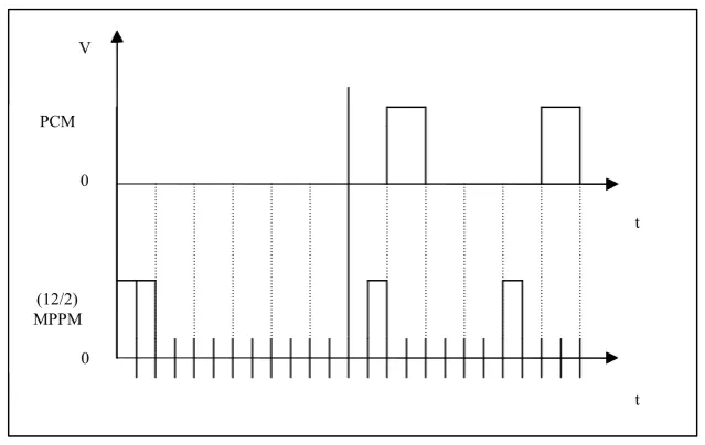
Fig. 2.1: Conversion of 3 bits of PCM (top trace) to multiple PPM (bottom trace).
PCM MPPM
000 00011
001 00101
010 01001
011 10001
100 00110
101 01010
110 10010
111 01100
PCM MPPM
V 0
0
t
Fig. 2.2: Conversion of 6 bits of PCM (top trace) to 12 bits multiple PPM (bottom trace).
2.5 Differential PPM
In 1984, Shirokov [13] presented Differential PPM (DPPM) and evaluated reliability when transmitted over optical fibre channels. In 1988, Zwillinger [14] proposed Differential PPM (DPPM) as a way to increase the throughput for a bandlimited and averagepowerlimited optical channel. Harddecision decoding of DPPM on photon counting channels was analysed by the same author. In the same year, Peile [15]
analysed Differential PPM with error correcting codes combined with interleaving techniques. In 1999 Dashan Shiu [16] also examined the use of DPPM for optical communication systems, using intensity modulation with direct detection in the presence of additive white Gaussian noise. He presented expressions for error probability and the power spectral density of the DPPM format. He concluded that for a given bandwidth, DPPM requires significantly less average power than pulseposition modulation (PPM); ISI penalties incurred by PPM and DPPM, exhibit very similar dependencies upon the channel delay spread. In 2008, Sethakaset and Guilliver [17]published a concatenation of
V
t
t PCM
0 (12/2) MPPM
marker and ReedSolomon codes in order to correct insertiondeletion errors in Differential pulseposition modulation. Code decoding algorithms with harddecision and softdecision detection were also presented.
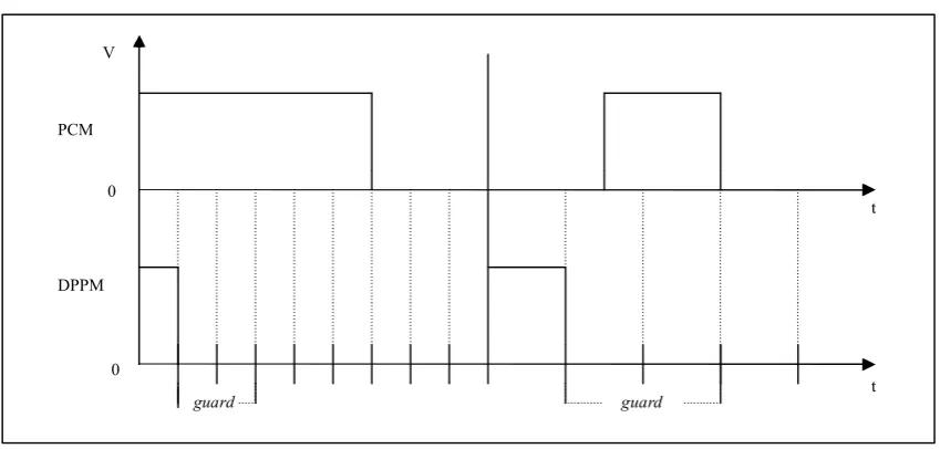
[image:41.595.87.512.465.668.2]DPPM Format
Table 2B and figure 2.3 present the relationship of the DPPM with PCM.
PCM DPPM
000 100
001 1000
010 10000
011 100000
100 1000000
101 10000000
110 100000000
111 1000000000
Table 2B: Differential PPM coding format.
Fig. 2.3: Conversion of 3 bits of PCM (top trace) to differential PPM (bottom trace).
PCM
DPPM V
0
0
t
t
2.6 DHPIM PIM, DPIM
In 1977, analytic and computer simulation results for a pulseinterval modulation (PIM) system, representing a discrete PPM system were published. [1]. The laser power required to achieve a given bit error rate was presented. Gol’dsteyn and Frezinskiy [2]
theoretically investigated this modulation format a year later. A complete noise performance analysis for a PIM system was published in 1983 by Marougi and Sayhood
[3]. Although PPM schemes offer an improvement in power efficiency, this is achieved at the expense of relatively poor bandwidth efficiency. Most PPM formats require symbol and slot synchronisation. Pulse interval modulation (PIM) requires no symbol synchronisation, while offering an improvement in bandwidth efficiency[1819].
presented complete derivations of the slot and packet error rates, optical and bandwidth requirements and confirmed calculated results through computing simulation.
PIM, DPIM & DHPIM Formats
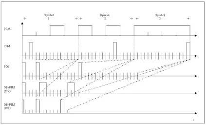
[image:43.595.87.511.262.518.2]Figure 2.4 presents PPM, PIM, DHPIM (a=2) and DHPIM (a=1) sequences in comparison with a PCM sequence.
Fig. 2.4: Conversion of 4 bits of PCM (top trace) to digital PPM (2 nd top trace), to PIM (3 rd top trace), to DHPIM (4 th and 5 th bottom trace).
2.7 Digital PPM
In several publications [8083], the spectrum of digital PPM has been presented and analysed. Elmirghani [83] presented a characterization of optical fibre digital PPM based on cyclostationary properties. He stated that optical fibre PPM, unlike satellite PPM, can exhibit discrete components at frame repetition rate. He also developed an original characterization for the cyclostationary PPM format, when impaired by timing jitter [94 95].
In 1998, Win [96] presented an analysis of digital PPM power spectral density (PSD). Win generated expressions for the PSD of digital pulse streams using wide sense cyclostationary (WSCS) sequences, in the presence of arbitrary timing jitter; methods based on stochastic theory were employed. Setting the period of WSCS sequence equal to one, results were obtained for a wide sense stationary (WSS) sequence. It was concluded that asymmetry of timing jitter does not affect the PSD. Mathematical calculations and simulation results are presented. The following is an equation of continuous PSD from Win’s publication [93]:
( )
j flT
t
N
n a c
m K n l f f e
N f
P T f
S e p
2 1 , 2 ) , , ; ( 1 ) ( 1 - ¥ -¥ = =
å å
úû ù ê
ë é
DigPPM Format
Digital PPM and PCM relationship is shown in table 2C and figure 2.5.
Table 2C: Differential PPM coding format
Fig. 2.5: Conversion of 4 bits of PCM (top trace) to digital PPM (bottom trace).
PCM Digital PPM
000 0000 0001
001 0000 0010
010 0000 0100
011 0000 1000
100 0001 0000
101 0010 0000
110 0100 0000
111 1000 0000
V PCM
0 Digital PPM
0
t
2.8 Dicode technique
The dicode technique is not a PPM format. It is usually used in magnetic recording channels where bandwidth is limited. Nevertheless, reference to this technique and the presentation of its format is indispensable for the better understanding of the Dicode PPM (DiPPM) scheme.
In 1971, Kobayashi [97] published several coding techniques, including the dicode technique, for the transmission and recording of digital data. Additionally, he presented error detection and correction of codes intended to combat random, or burst noise. Peter Kabal [98] states that because in real systems, data is not truly random, selected input sequences could conceivably suffer severe error propagation; precoding is therefore unhelpful. In 2001, Mats Oberg [99] presented an analytical method for estimating the average Euclidean distance spectrum for a serially concatenated, trelliscoded partial response channel. The technique was applied to the dicode channel, with and without precoding.
been completed from Costa [103104]. Costa stated that when dispersion and Kerr included chirps are of the same size, an improvement in system performance is presented. Band limiting also has marginal benefits on signal propagation under SPM impact. When under strong SPM influence, dicode modulation formats, due to specific characteristics, demonstrate greater robustness.
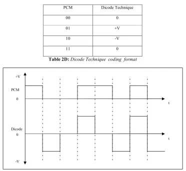
Dicode Technique Format
In dicode technique, data transitions are coded; no signal is transmitted when PCM data is constant. When PCM data transition turns from logic zero to logic one, the dicode is coded as +V and while PCM transition change from logic 1 to logic zero, the dicode is coded as –V (table 2D – fig. 2.6).
PCM Dicode Technique
00 0
01 +V
10 V
[image:47.595.112.485.357.699.2]11 0
Table 2D: Dicode Technique coding format
Fig. 2.6: Conversion of PCM (top trace) to dicode technique (bottom trace).
+V 0
0 V PCM
Dicode
t
Chapter 3
Dicode PPM
As presented in chapter 2, various pulse position modulation (PPM) schemes have been proposed for use in optical communication links. Although these schemes operate with higher data rates than their PCM counterparts, they offer greater sensitivity than PCM; with digital PPM providing a 5 to 11 dB improvement [5455, 5759, 63, 105]. The optimum receive filter for digital PPM consists of a noisewhitened matched filter and a proportional derivative delay (PDD) network [5455, 105]. As this PDD network is adjusted for individual links, implementation is complicated.
and digital PPM. Like digital PPM, Sibley’s new scheme offers greater sensitivity than PCM. However, unlike digital PPM, sensitivity is achieved with only a fourfold (DiPPM ISI) or twice (DiPPM) increase in speed. Although this Thesis (measurements, theories, simulations, mathematics, outcomes etc.) presents only DiPPM (without intersymbol interference (ISI)), it will be helpful the original form (DiPPMISI) of the dicode PPM scheme to be analysed first.
3.1 Dicode PPM with ISI guards (DiPPMISI)
Fig. 3.1: Conversion of PCM (top trace) to dicode technique (middle trace) and DiPPMISI (bottom trace).
In DiPPMISI, the SET and RESET signals are converted into two pulse positions in a data frame. Thus, a PCM transition from zero to one produces a pulse in slot S and a one to zero transition generates a pulse in slot R (fig. 3.1). No pulse is transmitted when the PCM data is constant at either 1 or 0. Two guard slots are used to reduce the effects of intersymbol interference (ISI). When there is minimal ISI, zero guard slots are used. As four slots are used to transmit one bit of PCM, and the line rate is four times that of the original PCM, speed is reduced when compared to digital PPM. Hence, DiPPM can be used in dense wavelength division multiplexing (DWDM) systems because of low bandwidth.
3.1.1 DiPPMISI Error Sources and Probabilities
+V 0 +V 0 V +V 0
S R G G S R G G S R G G S R G G S R G G PCM
Dicode Technique
DiPPM (ISI)
DiPPMISI uses a four symbol alphabet (table 3A); a typical sequence would be S, xN, R with symbol probabilities of 1/2,
( )
1 2x , 1/4 . The S signal has a probability of 1/2 because there are only two possible PCM sequences (00 or 01) after an R pulse has been transmitted. If the original PCM is line coded so that the run of like symbols is limited to n, the maximum DiPPM run would be R, nN, S. In this sequence, the S has a probability of one because it’s presence is guaranteed at the end of a run of n lots of N symbols.
Table 3A: DiPPMISI symbol alphabet.
ISI Included Error Probability.
In DiPPMISI, the shape of the S and R pulses will depend on transmitted pattern. The new pulse shapes, of a general DiPPM sequence S xN R yN S, are given by[29]:
(
, ,)
0( )
0 ( ( 3 4 ) s ) 0 ( ( 5 4 ) s )
oS x y t V t V t y T V t x T
V = + + + + - + (3.1)
(
, ,)
0( )
0 ( ( 5 4 ) s ) 0 ( ( 3 4 ) s )
oR x y t V t V t x T V t y T
V = + + + + - + (3.2)
Where only ISI between adjacent pulses has been considered. The general form of the equivalent PCM error probability, that considers a complete sequence for all x and y, is
[29]:
å å
- - + + + + ÷ ÷ ø ö ç ç è æ ÷ ø ö ç è æ ÷ ø ö ç è æ + ÷ ÷ ø ö ç ç è æ ÷ ø ö ç è æ ÷ ø ö ç è æ = 1 1 , , 2 1 , , 2 2 2 1 2 1 2 1 2 1 n y n x y n y n y n y x y x y xe P Error P Error
P n n n n n n n x n x n x n x Error P Error
P , ,
1 1 1 , , 1 2 2 1 2 1 2 1 2
1 + +
- + + ÷ ø ö ç è æ ÷ ø ö ç è æ + ÷ ÷ ø ö ç ç è æ ÷ ø ö ç è æ ÷ ø ö ç è æ
+
å
(3.3)
Where Px , y is the probability of a particular error event occurring and Errorx , y is the number of PCM errors the event generates. The lower x and y limits depend on the type of error being considered, while the factor n is included to account for the linecoding of the PCM data [29].
Detection errors that occur in DiPPM systems in the presence of significant ISI, are the same as digital PPM: wrongslot, erasure and false alarm.
Wrongslot Errors
Wrongslot errors occur when noise on the rising edge of a detected pulse causes the pulse to appear in adjacent time slots. In order to minimise this error, the pulse is detected in the centre of the time slot width Ts . Thus, errors are generated when the edge moves by Ts 2 . The probability Ps of a pulse appearing in the preceding slot is given by [27, 29]: ) 2 ( 5 .
0 s
s
Q erfc
P = (3.4)
2 0
) ( 2 n
t slope T
Q s d
s = (3.5)
2 0
n is the mean square noise of the receiver, and slope ( t ) is the slope of the received d
pulse at the threshold crossing instant, t .The presence of ISI means the slope of the d
pulse is different for S and R pulses and this must be accounted for by differentiating either (3.1) or (3.2) with respect to time.
A wrongslot event can cause four possible errors in DiPPMISI. If the pulse appears in slot S, noise can cause the edge to appear in the preceding guard slot or in the following R slot. In the first case, no detection error occurs because the preceding slot is a guard and the decoder will not recognize the false threshold crossing. In addition, as the pulse is still present in the S slot, it will be detected correctly. In the second case, the S pulse appears in an R slot and this leads to detection errors. The probability of this happening is
s
P as defined by equation (3.4) using the slope of the pulse defined by (3.1). This error causes the current PCM bit, and all following bits, to be in error until an R pulse is received. If the number of following N signals is x, the transmitted and received sequences would be as given in Table 3.B. Thus, (x+1) PCM errors are generated. The equivalent PCM error probability is given by (3.3) with x=0 and y=0 as the lower limits of the summations.
Table 3.B: Transmitted and received sequences with a wrongslot error.
Transmitted S xN R
Received R xN R
x
When the pulse is in the R slot, the slope must be obtained using the pulse defined by (3.2). This pulse could appear in the preceding S slot or the following guard slot, with (y+1) PCM errors resulting in both cases. The probability of error is given by (3.3) with x=0 and y=0 as the lower limits of the summations.
Erasure Errors
Erasure errors occur when noise is so great as to reduce peak signal voltage to below threshold level. The probability of this error is [27, 29]:
÷ ø ö ç è æ =
2 5
.
0 er
er
Q erfc
P (3.6)
where
2 0
n v v Q er pk d
-
= (3.7)
pk
v is the peak signal voltage at the output of the receiver for either an S or R pulse and
d
generates the same number of PCM errors. Hence, PCM error probability for erasure is [27]:
(
)
÷ ÷ ø ö ç ç è æ + ÷ ø ö ç è æ + + ÷ ø ö ç è æ=
å
- = + + 1 0 2 3 1 2 1 ) 1 ( 2 1 2 n x er n er x
erDiPPM P x P n
P (3.8)
False Alarm Errors
Due to ISI, there can be a signal voltage in the slots surrounding the one containing a pulse. Noise on this voltage can lead to a thresholdcrossing event when no pulse is presented; so called false alarm errors. Although there are many different types of ISI induced false alarm present in DiPPMISI, only the most significant have been considered. The error involved is minimal. The probability of false alarm error in DiPPMISI is [27, 29]:
÷ ÷ ø ö ç ç è æ = 2 5 .
0 f
t
Q erfc
P (3.9)
where
( )
2 0 0 n t v v
Q d d
f
-
= (3.10)
The number of uncorrelated samples per time slot can be approximated to Ts t R where
R
t is the time at which the autocorrelation function of the receive filter has reduced. The probability of a false alarm error then becomes [27, 29]:
÷ ø ö ç è æ = 2 5 .
0 t
R s f Q erfc T P
t (3.11)
Simulations performed using all possible sources of ISIinduced errors, indicate that the major source of error is an R pulse spreading into the S slot immediately before it. Further sources of ISIinduced errors can be neglected as they involve pulse spreading over several time slots and the effect is therefore minimal [27, 29].
If a pulse in slot R generates a voltage in the S slot immediately before it, the decoder will register an S pulse before the arrival of the pulse leading to (y+1) PCM errors. The ISI voltage in the S slot comes from the preceding S pulse, the current R pulse and the following S pulse. Thus [29]
(
)
(
)
[
]
2 0 0
0 4 4
n yT t v xT t v v
Q fr d d s d s
- +
+ -
= (3.12)
The equivalent PCM error probability, PefR -Ts , is obtained by substituting (3.12) into
False alarms can occur without ISI in the interval between the R pulse and the S pulse. Thus [29] 2 0 / n v Q d R S
fN® = (3.13)
The severity of the decoding error depends on where the false alarm error occurs in the string of N symbols. If the kth N symbol is in error, the equivalent PCM error probability is [29] ) 1 ( 2 1 2 ) 1 ( 2 1 2 / 2 1 / 3 1 1 1
/ P y k P n k
P fN S R
n n k R S fN y n y y k R S
efN ÷ + -
ø ö ç è æ + - + ÷ ø ö ç è æ = ® + = ® + - = =
®
å å
å
(3.14)where PfN ® S /R is the probability of a false alarm in either the S or R slot of a blank
frame, obtained using (3.13) and (3.12). The factor of two appears because a false alarm in an S slot has the same effect as one in an R slot
3.1.2 DiPPM (ISI)PINFET Receiver
In