Nisbet, Gareth
Structure analysis of adsorbates on single crystal surfaces using photoelectron diffraction
Original Citation
Nisbet, Gareth (2007) Structure analysis of adsorbates on single crystal surfaces using
photoelectron diffraction. Doctoral thesis, The University of Huddersfield in collaboration with the FritzHaberInstitut der MaxPlanckGesellschaft.
This version is available at http://eprints.hud.ac.uk/id/eprint/720/
The University Repository is a digital collection of the research output of the University, available on Open Access. Copyright and Moral Rights for the items on this site are retained by the individual author and/or other copyright owners. Users may access full items free of charge; copies of full text items generally can be reproduced, displayed or performed and given to third parties in any format or medium for personal research or study, educational or notforprofit purposes without prior permission or charge, provided:
• The authors, title and full bibliographic details is credited in any copy;
• A hyperlink and/or URL is included for the original metadata page; and
• The content is not changed in any way.
For more information, including our policy and submission procedure, please contact the Repository Team at: [email protected].
Structure Analysis of Adsorbates on Single Crystal
Surfaces using
Photoelectron Diffraction
Gareth Nisbet
Supervised by Dr C.L.A. Lamont
A thesis submitted to the University of Huddersfield in partial fulfilment of the requirements for
the degree of Doctor of Philosophy
The University of Huddersfield in collaboration with the Fritz-Haber-Institut der Max-Planck-Gesellschaft
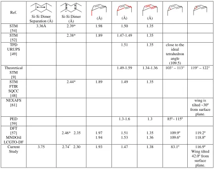
The structural determination of the Pt(111)c(5x√3)rect.-CO phase formed by 0.6 ML of adsorbed CO has been undertaken using scanned-energy mode photoelectron diffraction utilising the two distinct components of the C 1s photoemission peak. Earlier assignments of CO to atop and bridge sites have been confirmed as well as the respective 2:1 ratio of these assignments. Additionally, quantitative local structural details have been obtained. In particular, the Pt-C chemisorption bond lengths for the atop and bridging sites are 1.86 ± 0.02 Å and 2.02 ± 0.04 Å respectively. These values are similar to those obtained in previous studies for the 0.5 ML coverage c(4 x 2) phase involving an atop:bridge occupation ratio of 1:1. The results also indicate a definite tilt in the atop CO species of 10.7º +1.5º/-3.1º consistent with earlier investigations using electron-stimulated desorption ion angular distribution, LEED, Monte Carlo simulations and IR.
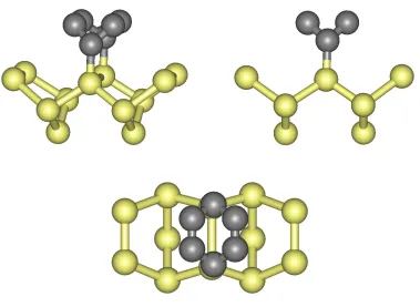
The local structure of benzene adsorbed on Si(001) has also been investigated using scanned energy photoelectron diffraction. The standard butterfly (SB), tilted (T), tight bridge (TB), pedestal (P), twisted bridge (TB), and diagonal bridge butterfly (DDB) models were optimized and compared with the lowest R-factors being achieved for SB and TB models (0.2337 and 0.2641 respectively). Further optimization was performed for a mixed overlayer (0.25 ML) consisting of SB and TB structures in various proportions. A significant improvement in the R-factor was achieved for a combined model in which 58 ± 35 % of the overlayer is composed of the SB structure.
Using the structural data for the CO/Pt(111), and benzene/Si(001) adsorption systems, comparative simulations have been undertaken to explore the effect of using vertically and horizontally polarized radiation on PhD modulation amplitudes and more importantly the sensitivity of each method to various structural parameters.
1 Introduction ... 5
2 Theory ... 7
2.1 XPS (X-ray Photoelectron Spectroscopy) ... 7
2.1.1 Principles of XPS... 7
2.1.2 XPS Measurements... 9
2.2 X-Ray Photoelectron Diffraction... 10
2.2.1 XPD ... 11
2.2.2 PhD ... 13
2.3 PhD Measurements... 15
2.4 Analysis of PhD Data ... 17
2.5 LEED... 20
2.5.1 Overlayer Notation ... 22
3 Hardware ... 24
3.1 Synchrotron Radiation Source... 24
3.2 Monochromator ... 27
3.3 The Chamber ... 28
3.4 Electron Energy Analyser... 30
4 Surface Structure of Pt(111)c(5x√3)rect.3CO at 0.6 ML Coverage ... 33
4.1 Introduction ... 33
4.1.1 Adsorption Sites and Periodicity ... 33
4.1.2 Bond Lengths... 38
4.1.3 Adsorbate Tilt ... 39
4.1.4 Relaxation... 39
4.2 Aim... 40
4.3 Experimental... 40
4.3.1 Sample Preparation... 40
4.3.2 PhD Measurements on CO Adsorbed on Pt(111) ... 43
4.4 Results and Discussion ... 45
4.5 Conclusion... 61
5 Surface Structure of Si(001)(2x2)-C6H6... 62
5.1 Introduction ... 62
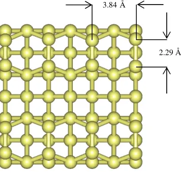
5.1.1 Clean Si(001)... 62
5.1.2 Benzene Adsorption... 63
5.1.3 Low Coverage... 64
5.1.4 Saturation Coverage... 65
5.2 Experimental Details ... 67
5.3 Results and Discussion ... 69
5.3 Results and Discussion ... 70
5.3.1 Standard Butterfly (SB) ... 70
5.3.2 Tilted (T)... 72
5.3.3 Tight Bridge (TB)... 73
5.3.7 Combined SB and TB... 78
5.4 Conclusion... 92
6 The Use of Vertically Polarized Radiation in PhD... 94
6.1 Introduction ... 94
6.1.1 Effects of Polarization on Spherical Waves... 94
6.2 Aim... 104
6.3 Results and Discussion ... 104
6.3.1 CO Adsorption on Pt(111)... 104
6.3.2 Benzene Adsorption on Si(001)... 119
6.3 Conclusion... 128
7 Conclusion and Future Work... 130
1 Introduction
A major driving force for studying chemical reactions on surfaces is the need to understand heterogeneous catalysis. The sheer scale of the subject’s significance can be expressed in the fact that heterogeneous catalysis is involved in literally billions of pounds worth of economic activity [1].
A catalyst is ‘an active chemical spectator’ [2], while it speeds up a reaction it cannot affect the position of equilibrium of a reversible reaction, and is chemically unchanged at the end of the reaction. A good catalyst can not only speed up a reaction but can do it selectively.
Heterogeneous reactions occur at the interface between systems in different phases. Gas-solid and liquid-solid interfaces are of particular interest because it is on the solid surface that catalytic substances can be deposited (if the solid, itself, is not the catalyst) and thereby immobilised. The obvious benefit of this is that the catalyst isn’t lost in the stream of products resulting in expensive recovery techniques. Furthermore, for some applications outside of the lab or chemical plant such as catalytic converters in car exhaust systems, the use of heterogeneous catalysis is essential.
A better understanding of heterogeneous catalysis may lie in the accurate structural determination of relevant surfaces and the molecules adsorbed on them. To this end, a detailed structural analysis of the economically significant CO/Pt adsorption system has been undertaken, more specifically CO adsorption on Pt(111).
Another area of surface science which is of increasing interest is the area of nanotechnology especially in the context of the semiconductor industry which in February 2006 accounted for an annualised $238 billion in global sales [3]. Gordon Moore, a co-founder of Intel made an observation in 1965 which has now become known as Moore’s Law. Moore’s Law states that in effect the progress of technological development is such that, the complexity of integrated circuits (IC) doubles every 18 months. This was revised in 1975 allowing two years for each technological leap [4, 5].
Recent AMD (Advanced Micro Devices) technology utilises copper interconnects which previously proved impossible to implement since the copper was found to diffuse into the silicon dioxide layers [6]. When critical dimensions in the region of 62 nm are required, this becomes a significant problem. However the problem has been circumvented by coating the chip with a barrier layer after photolithography [7] to prevent the copper from reacting with the silicon dioxide. As the miniaturisation of IC technology continues further, the interfacial areas will undoubtedly increase with respect to the bulk material, highlighting the necessity of atomic scale surface analysis. One of the problems that naturally arise with increased IC complexity and faster clock cycles is that of heat dissipation; the lack of which can have a detrimental effect on the semiconducting properties of silicon based semiconductors. While this can be resolved to some extent by the use of various heat dissipation techniques such as pneumatic or liquid (water or liquid nitrogen) cooling, another approach is to use a semiconductor which is more stable at higher temperatures. A strong candidate material for such a semiconductor is diamond [8]. Diamond is a wide band-gap semiconductor and as such retains its semiconducting properties at higher temperatures. The diamond can be produced artificially by heating ordinary carbon to around 1500 K under a pressure of 50,000 bar but this is an expensive process. Another method is to use chemical vapour deposition to build the diamond on a suitable substrate. One potentially suitable precursor for this process is benzene adsorbed on Si(001) [9]. An important step in ascertaining the suitability of such a system for this application is the detailed determination of the adsorption behaviour and structure. This has been undertaken in this thesis and is detailed in chapter 5.
The aim of this project is in part, the structural determination of the above mentioned adsorbate/substrate systems using PhD, and also to use the analysis of these systems to explore the feasibility of a new technique built upon PhD using out of plane polarized radiation. As will be discussed in section 2.2.2, PhD uses the interference between a directly emitted reference wave component and the scattered wave components. However when analysing systems in which the substrate is a weak photoelectron scatterer such as Pt or Si, the reference wave can be excessively dominant meaning some of the finer structural details can be lost. By using out of plane polarized radiation the reference wave is removed altogether leaving only the scattered components and thereby potentially exposing previously inaccessible structural information (see chapter 6).
Before these aims can be meaningfully discussed some background to the theoretical concepts of XPS, PhD and LEED is necessary.
2 Theory
2.1 XPS (X-ray Photoelectron Spectroscopy)
2.1.1 Principles of XPS
Core level electrons have a binding energy corresponding to that of photons in the soft X-ray region. When a material absorbs a photon with an energy greater than the binding energy of a core level electron, the electron, now referred to as a photoelectron, is ejected. The binding energy and the photon energy are related by the equation:
EK = hν - EB 222.1 2
Where: EK = Kinetic energy of the photoelectron (J)
h = Planks Constant (6.6261x10⁻³⁴J.s) ν = Frequency of photon radiation (Hz) EB = Binding Energy (J)
In order for photoemission to occur, the photoelectron must possess sufficient energy not only to free itself from the atom but also from the material’s surface. This additional energy is equal
EK = hν -EB -φ
2.2
Where: φ = Work Function (J)
The energies involved in equations 2.1 and 2.2 are small and are more conveniently expressed in electron volts (1 eV = 1.60219 x 10⁻¹⁹ J).
A typical value for the work function of a transition metal lies in the region of a few eV, for example 6.35, 5.01, 4.7 for Pt, Ni and Cu, respectively [10]. The use of the work function is complicated by the fact that it is not only a property of the material but also the geometry of the material’s surface and whatever atoms or molecules are adsorbed onto it. However, while significant, the work function for a given material is small, and the variations even smaller, when compared with the differences in the core level binding energies for any successive element and certainly for those used in this project. For example, C 1s, N 1s, and O 1s have respective binding energies of 284.2 eV, 409.9 eV and 543.1 eV [11].
Deep core electrons do not participate in bonding and are therefore characteristic of the atoms from which they come, thus making XPS an excellent tool for elemental analysis. In addition to this, XPS can distinguish between different species of the same element. This is possible due to small yet detectable shifts in the core level binding energies. These chemical shifts depend on the atom’s environment and in particular, the oxidation state of the atom [12]. This can be explained by the following argument.
The electron binding energy, EB, is given by the Einstein equation:
EB = hν – EK 2.3
This is simply a rearrangement of equation 2.1 but can also be expressed in terms of the energy difference between the initial and final energy states of the atom,
where Ei(n) is the initial state energy and Ef(n-1) is the final state energy. If there was no
relaxation of the spectator electrons and no extra-atomic relaxation, the binding energy would simply be equal to the negative of the orbital energy of the initial state of the electron and only a single peak for a given element would be observed. The fact that this is not the case is what gives XPS its extra versatility. The atom does experience electronic relaxation along with some extra-atomic relaxation, factors which are both influenced by the atom’s coordination. The extent of this influence is manifested in a shift in the binding energy. In general, the binding energy increases with oxidation state and with the electron withdrawing power of the substituents bound to the atom.
2.1.2 XPS Measurements
2.2 X-Ray Photoelectron Diffraction
When the directly emitted component and the scattered component of a photoelectron interact, they add together, by way of superposition resulting in constructive and destructive interference. A diffraction pattern is produced which is characteristic of the photoelectron
Fig.2.1 XPS for Pt (111) measured with a photon energy of 700 eV. The C 2s, O 2s and O 2p with binding energies of 7 eV, 18.2 eV and 23.1 eV respectively, are too weak to be visible at this magnification.
Fig.2.2 C 1s XPS spectrum showing the chemical shift for CO adsorbed in two different sites on Pt(111), namely atop and bridge. The spectrum represents the kinetic energy of the photo-emitted C 1s electrons for each species measured with a photon energy of 450eV.
Kinetic Energy eV
180 175
170 165
160 155
Experimental Data
Bridge Atop
1.1
1.0
0.9
0.8
0.7 400
300
200
100
0
In
te
ns
ity
(
ar
b.
un
its
)
700 600
500 400
300 200
100
O 1s
Kinetic Energy eV
Pt 4f5/2
Pt 4d3/2
Pt 4d5/2
Pt 4f7/2
sensitive to these parameters, when they are varied or scanned, XPS becomes X-ray photoelectron diffraction.
X-ray photoelectron diffraction can be divided into two sub-techniques namely, angle scanned photoelectron diffraction referred to as XPD, and scanned energy photoelectron diffraction referred to as PhD.
2.2.1 XPD
XPD is based on the use of a specific energy, optimised for the target material. The sample is rotated during the measurement (see fig.2.3) producing an angle dependent signature from which certain structural information can be inferred.
Fig.2.4 shows that the square modulus of the cross section, which determines the scattering
intensity in the absence of wave interference, is always at a maximum at 0o (the scattering atom
is between the emitting atom and the analyser (see fig.2.5).
Fig.2.3 The sample can be rotated about an angle θ (polar angle), changing the angle of incidence and emission, or about an angle φ (azimuth angle), changing the alignment of the crystal atoms and adsorbates with respect to the analyser.
θ
hν e-
φ
Fig.2.4 Modulus of the electron scattering factor of a Cu atom as a function of scattering angle for several different electron energies [13].
This is because the pathlengths for the directly emitted and scattered components of the photoelectron are the same, which always leads to constructive interference. Although, strictly speaking, the phase shift of the scattered component, which is energy dependant, influences the
Fig.2.5. Forward scattering (scattering at 0o) at normal emission. There is no
pathlength difference between the directly emitted component and the scattered component of the photoelectron.
Emitter
Emitted Component Scattered Component
1100 500 300 100 Kinetic Energy eV
0o 45o
90o 135o 180o
0.0 0.5 1.0
If
I/
If
(
Θ
=
0
)I
Scattering Angle, Θ
degree of constructive interference. The scattering cross section peak becomes more dominant
at 0o for higher energies as well as becoming sharper and thereby, more sensitive to the angle of
emission. This makes XPD an effective tool in the determination of molecular orientation, and the relative displacement of the substrate and overlayer atoms in ultra thin film growth [14]. XPD however only works in a two-atom situation were the emitter is distinguishable from substrate bulk such as the example depicted in fig.2.4. Overlayers composed of single atom adsorbates can be analysed through a chemical shift in the substrate atoms involved in adsorption. Although it is often the case, especially with physisorption, that no measurable chemical shift is observed. This problem is circumvented in PhD.
2.2.2 PhD
While XPD relies on forward scattering or zero order diffraction i.e. zero pathlength difference (see fig.2.4), PhD relies on back scattering and non-zero order diffraction, exploiting real
pathlength differences. At 180o, the backscattering direction (the emitting atom is between the
A 2D representation of the single electron model used to describe the diffraction in PhD is depicted in fig.2.6.
When a photoelectron is liberated, it can be emitted in any direction, the probability of which can be represented two dimensionally by concentric circles about the emitting atom. The circles represent a given phase in the wave cycle of the photoelectron. The scattered component of the photoelectron can be represented in the same way with concentric circles about the scattering atoms. However, due to a difference in the pathlength and a phase shift resulting from the photoelectron’s interaction with the scattering atom, the scattered component will emerge out of phase with the directly emitted component. When the energy dependence of the constructive and destructive interference arising from this phase difference is analysed for several emission angles using synchrotron radiation, very precise structural information about the emitter and its local environment can be deduced. Such information includes nearest neighbour bond lengths, molecular orientation, relaxation and reconstruction.
Detector
Emitted Component
Single scattered component X-rays (hν)
Substrate Emitter
2.3 PhD Measurements
A PhD spectrum consists of a succession of energy distribution curves (EDCs) (fig.2.7).
An EDC is a measurement of photoelectron intensity as a function of energy for a specific photon energy. Each EDC is measured around the core level peak with a suitable window allowing for the necessary background levels to be included. When the background is extrapolated to remove low amplitude noise, individual peaks in each EDC can be fitted and integrated to give the peak intensity. This is done using a Gaussian function modified with a step to compensate for the differences in background height either side of the peak.
600 500 400 300 200 100 x 1 0 3 350 300 250 200 150 100 PhD Spectrum EDC
Fig.2.7 A PhD spectrum with an expanded EDC for the C 1s photoelectrons of different species of CO on Pt(111) taken at a temperature of 130K.
I nt en si ty ( A rb . U ni ts ) 1.1 1.0 0.9 0.8 0.7 180 175 170 165 160 155 Fit Experimental Data
Kinetic Energy (eV)
10000 8000 6000 4000 2000 0 214 212 210 208 206
Fig. 2.8 High resolution XPS spectrum for C 1s measured with a photon energy of 500eV. The peaks labelled A and B correspond to the C 1s peaks for the atop and bridge species respectively. The features of this spectrum will be discussed in section 4.3.1.
Kinetic Energy (eV)
I nt en si ty ( A rb . U ni ts )
It is often the case, as mentioned earlier, that the chemical shift is not sufficiently large to prevent some overlap in the peaks for different species of the same element. This is the case for the example represented in fig.2.8, however, when enough of the peak profile can be resolved, it is possible to obtain an acceptable integration of the peaks. Once this is done the integrals of
individual peaks for each EDC can be separated out and their intensities (I(Ekin)) can be plotted
against the kinetic energy for the entire PhD spectrum (fig.2.9).
There are some intrinsic influences on the experiment which must be accounted for. As previously mentioned, PhD requires the use of synchrotron radiation. The electron current produced by the synchrotron has a half life of a few hours which significantly reduces the X-ray flux density over the duration of the PhD scan which takes about two hours. In addition to this, the reflective properties of the monochromator must be accounted for. The monochromator is effectively a plane mirror with a diffraction grating (either 400 or 1200 lines per mm). The mirror exhibits different degrees of reflectivity depending on the energy of the incident radiation thereby directly affecting the flux density of the beam. A third influencing factor is the variation of the photoionisation cross section as a function of photon energy.
Compensation for these influences can be made by using an appropriate software package such as Igor (also used to integrate the peaks) to fit a smoothing spline function to the data (fig.2.9).
1.4
1.2
1.0
0.8
0.6
0.4
0.2
350 300
250 200
150 100
Kinetic Energy (eV)
Intensity I(Ekin)
Smoothing spline I0(Ekin)
In
te
ns
ity
(
ar
b.
u
ni
ts
)
(
)
(
)
(
E
)
I
I
E
E
I
kin 0
kin 0 kin
χ= − 2.5
Where I(Ekin) is the data intensity at the kinetic energy Ekin, and I0(Ekin) is the intensity of the
spline function at the kinetic energy Ekin. The result is a modulation function (fig. 2.10), also
known as a chi (χ) curve.
2.4 Analysis of PhD Data
A quantitative structural analysis is achieved through trial-and-error modelling, simulating the experimental data with multiple scattering calculations for various trial structures. These
calculations are performed with codes developed by Fritzsche [15-1617], which are based on the
expansion of the final state wave-function into a sum over all scattering pathways which the electron can take from the emitter atom to the detector outside the sample. A magnetic quantum number expansion of the free electron propagator is used to calculate the scattering contribution of an individual scattering path. Double and higher order scattering events are treated by means of the Reduced Angular Momentum Expansion (RAME) [18]. The finite energy resolution and angular acceptance of the electron energy analyser are accounted for analytically. Anisotropic
-0.20 -0.15 -0.10 -0.05 0.00 0.05 0.10
350 300
250 200
150 100
M
od
ul
at
io
n
fu
nc
tio
n
(a
rb
. U
ni
ts
)
Fig. 2.10Modulation function χ derived from the intensity versus kinetic energy curve depicted in fig .2.9.
vibrations for the emitter atom and isotropic vibrations for the scattering atoms are also taken into account.
First, the crystal structure of the substrate is defined by giving the position of one atom and defining 3 translation vectors. Thus a 3D network is generated, creating a hemispherical cluster with a radius of 30 Å. The adsorbate molecules are then defined with respect to the substrate in positions roughly deduced from a direct analysis of the experimental modulation functions (see chapter 4). The periodicity of the adsorbate overlayer is often known from LEED experiments and can be reproduced in the simulation program using 2D translation vectors. Once the general cluster has been defined, the theoretical model is compared with the experimental one using an objective reliability factor or R-factor. Equation 2.6 produces an R-factor comparing the experimental modulation function with the simulated modulation function for a single spectrum.
(
)
(
)
∑
∑
= = χ + χ χ − χ = m 1 i 2 i Kj th 2 i Kj exp m 1 i 2 i Kj th i Kj exp ) E ( ) E ( ) E ( ) E ( R 2.6WhereχKjexp(Ei) is the intensity of the experimental modulation function at the point i, and m is the number of points in the modulation function.
The global R-factor, R global, is of the same form but includes all of the spectra.
(
)
χ + χ ∑ ∑ χ − χ ∑ ∑ = = = = = 2 i K th 2 i Kj exp m 1 i n 1 j 2 i Kj th i Kj exp m 1 i n 1 j global ) E ( ) E ( ) E ( ) E ( R j2.7
Where Kj is the direction of the emitted electrons for a given spectrum, j, and n is the total
stronger modulations, have more of an influence over the global R-factor. An R-factor of 0 represents perfect correlation between the experimental and theoretical modulation function, a value of 1 implies no correlation and a value of 2 means there is anti-correlation. Usually the starting model shows little or no correlation, and so the parameters must be optimised. This is done in two ways. Firstly, a series of line scans are carried out. These involve scanning a variable (sometimes 2 or 3 when the variables are coupled) over a selected range with an appropriate step size until a minimum R-factor is reached. This is repeated for all the defining parameters which include, bond lengths, bond angles, interlayer separation, surface relaxation and reconstruction parameters, and vibrational amplitudes. Secondly, the fitting procedure is carried out. This is directed by the program itself, which searches for the minimum R-factor by improving the value of selected parameters. The fitting procedure is only carried out after the line scans to prevent the program optimising about a false local minimum. The evolution of the R-factor could be represented as a succession of peaks and troughs. A local minimum R-factor would be the bottom of a trough but not the deepest trough.
PhD, like any surface science technique, is more sensitive to certain parameters than others. An indication of the precision to which these parameters can be determined, can be obtained via a
calculation of the variance [19] in the minimum R-factor (Rmin).
(
)
N 2 R R
var min = min 2.8
Where N is the number of independent pieces of structural information contained in the data and is given by:
2 b 2 Oi E V 4
δE n
N
+ ×
= 2.9
δE is the energy range of the spectra, n is the number of spectra used, VOi is the imaginary part
of the inner potential, taken to be 5 eV, and Eb is the energy broadening factor, also taken to be
5 eV.
values and taking the interval containing the parameter values with an R-factor below Rmin+var(Rmin) (see fig. 2.11).
2.5 LEED
LEED (low energy electron diffraction) is a well established technique which can involve, like PhD, the use of complex simulations and even more extensive data sets. However, in its simplest form it can give a visible diffraction pattern of the corresponding periodicity of the reciprocal mesh of the surface. This can be viewed on a fluorescent screen directly without the need of any data analysis. As well as providing an elegant method of determining the periodicity of the surface, the diffraction pattern can be used to determine the azimuthal orientation of the crystal.
LEED experiments are performed by directing a beam of electrons of a well-defined low energy (typically in the range 20 - 200 eV) at normal incidence to the sample. The sample itself must be a single crystal with a well-ordered surface structure in order to generate a back-scattered electron diffraction pattern. A typical experimental set-up is schematized in fig. 2.12.
Fig. 2.11 Variance graph for Pt-C bondlength. In this case Rmin+var(Rmin) was calculated to
be 0.3445. The Rmin+var(Rmin) line intersects the Pt-C curve at 1.816 Å and 1.872 Å any
value between these points is within the error limits for this parameter.
Variance
0.29 0.34 0.39 0.44 0.49 0.54
1.75 1.8 1.85 1.9 1.95
Pt-C atop bond length
The electrons are scattered both elastically and inelastically. The latter emerge from the sample with a reduced energy and are removed by the energy-filtering grids. Consequently, only the elastically-scattered electrons contribute to the diffraction pattern.
The positions of the diffraction spots are determined by the space lattice (i.e. by the size and shape of the unit cell) and are independent of the penetration depth of the electrons. The intensities are determined by the diffraction function (i.e. by the exact atomic coordinates
within the unit cell) and are a function of the electron penetration depth. The basis vectors a1
and a2 describe the unit cell in real space and define the smallest parallelogram from which the
surface can be reconstructed by simple translation. A reciprocal space representation of the real space lattice is defined by the basis vectors a1* and a2*. Introducing γ and γ* as the angles
between (a1 and a2) and (a1*and a2*) respectively (see fig.2.13), the relationship between the
real space and reciprocal space vectors can be expressed as follows.
2.10
γ
sin
a
1
a
1 * 1
=
Fig.2.12 Typical setup of electron gun, filtering grids, and fluorescent screen used in LEED experiments,
Retarding Potential -VE +V
Fluorescent Screen ~5kv
-VE
Electron Gun
2.11
sin γ = sin γ* = sin(180- γ) 2.12
The inverse relationship expressed here means that a short vector in real space corresponds to a long vector in reciprocal space. The diffraction pattern corresponds to reciprocal space and can easily be transposed using equations 2.10 and 2.11, to describe the real space lattice.
2.5.1 Overlayer Notation
There are two conventions for naming overlayer structures. The first of these, Wood’s notation, relates the overlayer mesh to the substrate mesh and can be describe by the form:
Where M = the chemical symbol for the substrate; (hkl) = the miller indices of the surface plane; c or p = centred or primitive unit cell (if primitive, the p is usually dropped); |as| and |bs|
= the magnitude of the substrate vectors; |ao| and |bo| = the magnitude of the overlayer vectors;
α = angle between the overlayer and substrate meshes; and A = the chemical symbol for the
overlayer species.
γ
sin a
1 a
2 *
2 =
A R
b b a a p) or c )(
M( o
s o
s
o − −
×
α
hkl
γ
*a2*
a1*
γ
a2a1
The second convention for naming overlayer structures is to use the matrix notation. Taking the example depicted in fig.2.14, the primitive mesh vectors of the substrate (as and bs) can be used
by way of a linear combination to define the overlayer mesh vectors (a1 and b1).
ao = 1as + 1bs
2.13
bo = -1as + 1bs
2.14
2.15
Where the matrix;
−1 1
1
1 defines the overlayer mesh in terms of the substrate. The full matrix
notation in this example is then, Cu (100) -
−1 1
1
1 – CO. Wood’s will be used throughout this
thesis.
Fig.2.14Example of a Cu (100) - c(2 x 2) – CO or Cu (100) - (√2 x √2)R45o - CO as described by Wood’s notation. Note that a1 and b1 can be measured in terms of
either a centred or primitive unit cell in this example.
−
=
s s
o o
a
a
1
1
1
1
b
a
bs
ao
bo
ao
bo
3 Hardware
3.1 Synchrotron Radiation Source
As its name suggests, scanned energy photoelectron diffraction requires a source of tuneable X-rays of a suitable intensity. Currently, the most effective way of achieving this is by the use of synchrotron radiation. BESSY II, a third generation synchrotron radiation source located in Berlin was used for this work.
When electrons are accelerated to relativistic velocities (velocities close to the velocity of light, c) and deflected by a magnetic field, electromagnetic radiation is produced tangentially to the arc of deflection. This is synchrotron radiation. Second generation synchrotron radiation sources consisted mainly of a microtron, a synchrotron, a storage ring and tangential beam lines. In the case of BESSY I, the electrons were produced from a hot cathode under ultra high
vacuum (UHV) and accelerated towards the anode with a voltage of about 105 V. The electrons
were further accelerated in a circular trajectory by a high frequency magnetic field in the microtron. Having achieved an energy of 22 MeV, the electrons entered the synchrotron and were further accelerated to an energy of 800 MeV which corresponds to an average velocity of 2.9979240x10⁸ ms-1 (c = 2.99792458x10⁸ ms-1). Finally the electrons were transferred to the
storage ring where their trajectory was maintained by magnetic fields (see fig.3.1).
When the orbiting electrons pass through a magnetic field they are deflected in a direction which is perpendicular to the magnetic field. The resulting synchrotron radiation is propagated
tangentially to the electron trajectory in a narrow radiation cone with an opening angle (∆φ)
Fig.3.1. A schematic diagram of the bending magnets such as those used in BESSY and BESSYII.
e 2
3.1
where 3.2
and 3.3
At BESSY II electrons are accelerated to an energy of 1.6 GeV corresponding to a velocity of
2.9979244x10⁸ ms-1 which, incidentally, due to a relativistic effect which can be explained in
terms of γ, is only 40 ms-1 faster than the electrons at BESSY I. Insertion devices, such as wigglers and undulators used in third generation synchrotrons, provide a way of exploiting the intrinsic brightness of the synchrotron-radiation source.
Both wigglers and undulators consist of a periodic array of magnets with alternating polarity. When the relativistic electron passes through these devices, its trajectory is changed at every magnet resulting in an oscillatory motion. Radiation is emitted tangentially to each curved trajectory and is added together in the forward direction as it proceeds along the device. This results in a beam intensity significantly greater than that achieved using bending magnets alone. The magnetic arrays used in wigglers (see fig.3.2) consist of fewer yet stronger magnets than those used in undulators causing deflections through an angle which is large when compared with the radiation cone normally associated with synchrotron radiation. The radiation produced covers a wide energy range exceeding even that produced by the bending magnets; however the brilliance is less due to the enlarged radiation cone.
2 2
c v 1
1
γ
− =
e 2
E mc
≅
∆
φ
-1
γ
≅
In contrast to wigglers, undulators use weak magnetic fields. As the electron beam passes longitudinally through the array, its trajectory oscillates in the horizontal plane. The relatively weak field of the undulator means the radiation cones emitted at each bend in the trajectory overlap, giving rise to a constructive interference effect. The result is a high intensity beam with one or a few spectrally narrow peaks of quasi-monochromatic radiation which can be tuned by altering the gap between pole tips (fig.3.3).
Electrons producing synchrotron radiation lose energy in the process. In addition, particles lose energy due to their interaction with the surrounding vacuum chamber walls. This energy needs to be restored to the electrons so that they can maintain a steady orbit. This is achieved when the electrons pass through the RF (radio frequency) cavity. Electrons entering the cavity in phase with the sinusoidal RF field are accelerated whilst those entering out of phase are subsequently scattered and lost. The inclusion of RF cavities allows the beam to be maintained at a useful intensity for several hours.
Fig.3.3 A schematic diagram of an undulator array such as that used in BESSYII and other third generation synchrotron radiation sources.
1/2 e
2
N E
mc e-
Fig.3.2. A schematic diagram of a wiggler array such as that used in BESSY II
and other third generation synchrotron radiation sources.
e 2
3.2 Monochromator
The monochromator facilitates the separation of the broad spectrum of synchrotron radiation into distinct wavelengths, and therefore energies, required for energy scanned experiments. When the electromagnetic radiation enters the beam line, it is collimated by a toroidal mirror and projected on to a plane mirror. The plane mirror is movable and works in tandem with the plane grating ensuring that it receives radiation at a well defined angle of incidence (see fig.3.4).
The plane grating divides the incoming beam into its constituent components (fig.3.5). The plane grating can be positioned so that only the desired ‘colour’ or energy continues through the beam line.
Fig.3.5 An example of how a beam of light can be separated into its constituent components using a diffraction grating. The plane gratings used in this work were 400 or 1200 lines per mm.
Fig.3.4 Diagram showing the radiation pathway through the UE56/2-PGM 1 beam line at BESSY II.
Undulator
Wall housing beamline entrance slit
Toroid Mirror
Plane Mirror
Plane Grating
Cylindrical Mirror
Chopper
Exit Slit
Cylindrical Mirror
Sample
Purple light composed of red and blue light Diffraction Grating
The monochromatic light is focused on the exit slit by a cylindrical mirror. A final cylindrical mirror is used after the exit slit, to focus the beam onto the sample creating a spot size of
20-200 µm (vertical) by 900µm (horizontal). At this point the beam intensity is very high and can
unduly influence the system to be analysed by causing desorption or molecular cracking. For this reason a 1.2 m extension tube was placed between the beam line and the chamber to displace the sample from the focal point. The change in spot size is only a few percent because the beam exhibits a high degree of parallelism.
3.3 The Chamber
The UHV (ultra high vacuum) apparatus consists of two chambers vertically arranged and separated by a gate valve (figs. 3.6 and 3.7).
Fig. 3.6Functional diagram of the UHV apparatus [20].
Turbo Pump Scroll Pump Titanium
Sublimation Pump 5 Axes Manipulator
Fig. 3.7 Cross sectional view of top and bottom chambers showing the positions of the mass spectrometer, ion gun, analyser and LEED apparatus.
Analyser
Bottom Chamber
To The Pumps To The
Beam Line Mass Spectrometer
LEED Ion Gun
From Gas Line
Top Chamber
To The Pumps
Both chambers operate with a base pressure of 10-10 mbar which is achieved using a combination of scroll, turbo and titanium sublimation pumps. The top chamber is used for preparation and is equipped with an ion gun, dosing facilities, a quadrupole mass spectrometer and a qualitative LEED system. The bottom chamber terminates the beam line and is fitted with an Omicron EA 125 HR electron energy analyser which is described in more detail below. A multidirectional manipulator is used to position the sample. The manipulator is capable of rotating the sample about the polar and azimuthal axis as well as moving in the x, y and z directions. It also provides an earth connection to the sample, replenishing the photo-emitted electrons, and a thermal connection allowing the sample to be cooled to about 140K using
liquid nitrogen (LN2) or about 60K using liquid helium (LHe). The sample can also be heated
using a tungsten filament positioned directly behind the sample which is set to a high voltage of around -500 V. Passing a current of about 5 A through the filament produces an emission current of around 30 mA.
3.4 Electron Energy Analyser
The Omicron EA 125 HR is a concentric hemispherical analyser (fig.3.8) and is comprised of an electrostatic lens, two negatively-charged concentric hemispheres, and a channeltron detection system.
The lens is used to collect, retard and focus the electrons. The electrons enter the hemispherical dispersing unit through the entrance slit. The electrons are exposed to an electric field resulting
from the negatively charged hemispheres (where U1 > U2) and are consequently deflected. The
extent of this deflection depends on the strength of the electric field and the energy of the
electrons. Only electrons in a narrow energy region (E ± δE) succeed in reaching the exit slit.
The width of this energy region (2δE) is known as the pass energy. Electrons with an energy
less than E – δE will be forced into the inner hemisphere by the greater potential of the outer
hemisphere. While those with an energy greater than E + δE are able to overcome the potential
of the outer hemisphere and are consequently terminated.
The analyser setup allows two basic modes of operation, namely the constant retarding ratio
mode, and the constant transmission mode. In the former the electrons are retarded by a fixed
potentials U1 and U2. In the latter mode, the mode used for this work, the potentials U1 and U2
are kept constant and the energy range is selected by varying the degree of retardation.
Fig.3.8 Schematic representation of the Omicron EA 125 HR electron energy analyser [21].
The electrons leaving through the exit slit are detected by an array of 7 channeltrons. A typical example of a channeltron is depicted in fig. 3.9. It consists of a specially formulated lead silicate glass, shaped like a cornucopia, and exhibits the properties of electrical conductivity and secondary electron emission. The input end (the cup) is at ground or some positive potential while the output end (the tail) is at high positive voltage. An electron striking the
E E + δE
-U1
R0
Entrance slits Exit slits
Electron path
Electrostatic lens
Sample Concentric hemisphere
Electron detector
Pulse amplifier
Converter
Computer -U2
input face of the cup produces 2-3 secondary electrons which in turn do the same. These electrons are accelerated down the channel by the positive bias causing a cascade generating a pulse of 107 to 108 electrons.
The use of more than one channeltron enables parallel detection, reducing the signal to noise ratio.
The analyser is mounted at 60o with respect to the incident radiation and lies in the plane of the
radiation polarization vector. This is done to maximise the signal, detecting both directly emitted and scattered photoelectrons. The consequences of positioning the analyser out of the polarization vector will be discussed in chapter 6.
Fig.3.9 The basic operation of a typical channeltron. Primary
electron
Non-conductive
region Integral bias resistor
Secondary electrons Emissive layer
(SiO2 10Å)
SiO2 200Å
Conductive Layer 2000Å
Bulk Glass
4 Surface Structure of Pt(111)c(5x√3)rect.3CO at 0.6 ML Coverage
4.1 Introduction
There have been numerous studies pertaining to the structural determination of CO adsorbed on Pt(111). This system is accredited with such importance because of its application as a catalyst
promoting the oxidation of CO to CO2 in car exhaust systems. Moreover, due to the simplicity
of the CO molecule, it is often used as a probe molecule in surface science. A better understanding of the catalytic properties of the CO/Pt(111) system depends on quantitative analysis of the system’s adsorption behaviour. Relevant aspects of this behaviour include parameters such as adsorption sites, periodicity, bond lengths, bond axis and substrate reconstruction and relaxation. These parameters have been analysed in this project for the
Pt(111)c(5x√3)rect.-3CO configuration resulting from a coverage of 0.6 ML.
4.1.1 Adsorption Sites and Periodicity
When analysing the structure of adsorbate/substrate systems, the first structural parameter to be considered is where the adsorbate will locate itself and, subsequently, with what periodicity. In the case of Pt(111), adsorption can occur at four possible adsorption sites, namely atop, bridge, and two inequivalent hollow sites (fig.4.1). The inequivalence of the hollow sites owes to the fact that Pt(111) exhibits an ABC periodicity in its layers meaning that one hollow site is situated directly above a Pt atom in the second layer while the other is situated directly above a Pt atom in the third layer, these are known as hcp and fcc hollow sites, respectively.
Atop site
Bridge Site
Fig.4.1. Types of adsorption sites on a Pt(111) surface.
Blackman et al. [22], using diffuse LEED, studied a disordered 1/3 monolayer at 160 K, and
concluded that 88% ± 5% of the molecules occupy atop sites while 12% ± 5% occupy bridge sites. They also indicated that a c(4x2)-2CO arrangement is formed at a coverage range of 0.35 - 0.5 ML at just below room temperature.
According to the electron energy loss spectroscopy (EELS) studies of Steininger et al. [23], CO
adsorbs preferentially on Pt(111) at atop sites forming a ( 3× 3)-R30o structure (fig.4.2) at
170 K which then evolves to a c(4x2) structure at higher coverage, corresponding to half a monolayer consisting of adsorbates occupying both atop and bridge sites (fig.4.3).
In their dynamical LEED intensity analysisof the CO/Pt(111) system at 150 K with a coverage
of 0.5 ML, Ogletree, Van Hove, and Somorjai [24] also found that CO adsorbed preferentially at atop and bridge sites.
These assignments were later confirmed by a dynamical LEED study [22] and further
substantiated by C.A Lucas et al. [25] using X-ray diffraction. M.Ø. Pedersen et al. [26] using scanning tunnelling microscopy (STM), also showed that two sites are occupied by CO at low
Pt O C
Fig.4.2. The Pt(111) ( 3× 3)-R30o arrangement. The same colour scheme will be used throughout,
coverage (0.5 ML), which, when compared with simulated STM images were accepted to be atop and bridge sites in a c(4x2)-2CO configuration which is observed at both 150 K and 300 K.
Petrova et al. [27] proposed a c(4x2)-2CO structure using the alternative notation (2x√
3)rect.-2CO assigning a 1:1 ratio of atop and bridge species at 170 K. However, in contrast to the findings of the preceding studies, they argued that the LEED pattern they obtained (Fig.4.4) was indicative of a configuration in which the bridge species occupy bridge sites which are not equidistant from the neighbouring occupied atop sites (see fig.4.5).
Fig.4.5. The Pt(111) c(4x2)-2CO arrangement Petrova et al. [27].
Petrova et al. [27] also investigated higher coverages and proposed a c(√3 x 5)rect.-3CO structure, comprised of atop and bridge species in a 1:2 ratio (see fig. 4.6), at a coverage of
0.6.ML. This corresponds to the LEED pattern shown in fig 4.7.
This assignment however, is contradictory to the findings of Persson et al. [28] who proposed
that as θ increases beyond 0.5 ML, the relative bridge coverage decreases so that at the point
when θ is equal to 1 ML, no bridge species remain. Their study undertaken at 50 K involved
the comparison of Monte Carlo simulations with LEED and infrared spectra, and resulted in the proposal of a c(5x√3)rect.-3CO overlayer in a 2:1 atop/bridge configuration (Fig.4.8). Their model is described as consisting of vertical strips of the c(4x2) structure forming a phase/antiphase sequence. The strips are separated by fault lines or domain walls consisting of higher density terminal CO molecules. Persson also points out that these CO molecules are displaced from the high-symmetry atop sites by ~0.4 Å due to the unbalanced repulsive intermolecular interactions.
Fig. 4.6. The c(√3 x 5)rect.3CO arrangement as proposed by Petrova et al [27] (based on a diagram presented in their paper).
Fig. 4.7. LEED pattern resulting from CO adsorbed on Pt(111) at a coverage of 0.6 ML [27].
[image:37.595.248.362.364.484.2]Avery [29], in his EELS study of CO on Pt(111) at 140 K reports a decrease in bridge species beyond a coverage of 0.5 ML which is in agreement with the findings of Persson et al. [28]
Avery also proposes a c(5x√3)rect.-3CO (see fig 4.9) overlayer which however, is neither in
agreement with the findings of Persson nor Petrova. Avery describes this configuration as consisting of strips of half-monolayer c(4x2) structures which are antiphase with adjacent strips across coherently spaced boundaries or packing faults.
The c(5x√3)rect.-3CO proposed by Persson et al. [28] is supported by the STM observations of
Song et al. [30]. While their analysis does not deal with a complete 0.6ML surface, they do observe domains of 0.5 ML and 0.6 ML coverage, corresponding to the c(4x2)-2CO and
c(5x√3)rect.-3CO configurations.
c(√3 x 5) rect.
Fig. 4.8. Schematic diagram of the c(√3 x 5)rect. phase for CO adsorption on Pt(111) at a nominal coverage of 0.6 proposed by Persson et al. [28].
Fig. 4.9. Image based on the c(5x√3) rect-3CO proposed by Avery [29].
4.1.2 Bond Lengths
In addition to the determination of the preferential adsorption sites and the periodicity, a determination of the inter-atomic bond lengths is necessary as this is a direct result of the chemical behaviour of the system and therefore bears some relevance to the catalytic processes involved.
Numerous studies have been undertaken with the aim of properly determining the inter-atomic bond lengths of the c(4x2)-2CO system. Using the fhi96md plane-wave DFT code, Alavi et al. [31] calculated a Pt-C bond length of 1.86 Å for atop sites and 1.94 Å for bridge sites for the c(4x2)-2CO system (Fig.4.2). The respective C-O bond lengths were computed to be 1.13 Å and 1.16 Å. A more recent DFT study by M. Lynch and P. Hu [32], reports a Pt-Catop bond
length of 1.85 Å, a Pt-Cbridge bond length of 2.01 Å and respective C-O bond lengths of 1.15 Å
and 1.18 Å. These values are in good agreement with the results of a LEED intensity study performed by Ogletree et al. [24]. Ogletree found the respective Pt-Catop and Pt-Cbridge bond
lengths to be 1.85 ± 0.05 Å and 2.01 ± 0.07 Å and the C-O bond lengths to be 1.15 ± 0.05 Å for both species. These values are presented again later in table 4.3.
Blackman et al. [22], in their diffuse LEED study, report Pt-C interlayer spacings of d┴top =
1.85 Å and d┴bridge = 1.55 Å which correspond to bond lengths of 1.85 Å and 2.08 Å,
respectively. The C-O bond lengths were taken to be 1.15 Å and perpendicular to the surface as reported by Ogletree.
M.Ø. Pedersen et al. [26], in their scanning tunnelling microscopy study, report Pt-Catop and
Pt-Cbridge bond lengths of 1.80 Å and 2.05 Å respectively. The corresponding C-O bond lengths
were both found to be 1.15 Å.
atop site has a Ni-CO bond length marginally longer (0.06 Å) than that for the same atop site in the strongly chemisorbed c(2x2)-CO phase despite a change in chemisorption bond strength of more than a factor of 2.
4.1.3 Adsorbate Tilt
In their ESDIAD study of the high coverage CO/Pt(111) system, Kiskinova et al. [34] presents evidence of tilting in the terminal-CO species of 6 ± 1º in the [112] equivalent directions. This, it is argued, is associated with the close packing of the terminal-CO in the fault line regions. The model upon which this argument is based is that proposed by Avery et al. [29] (fig 4.9). While this model is in dispute, the alternative model proposed by Persson et al. [26] (fig 4.8) bears similar characteristics in that there are regions in which the terminal-CO species occupy adjacent Pt sites. Persson suggests that the resulting repulsive intermolecular interactions causes a shifting of the CO molecules off the high symmetry atop positions by ~0.4 Å, which assuming the C-O bond axis points to the centre of the Ptatop atom, corresponds to a tilt of 10º.
4.1.4 Relaxation
While the aforementioned structural parameters can be interpreted as the effects of the substrate on the CO molecules, the effects of CO on substrate relaxation and reconstruction must also be considered. The surface of a substrate differs considerably from the bulk due to the fact that the surface atoms do not have their full coordination complement. The atoms, therefore, find themselves in a higher energy situation. In response to this, the surface undergoes relaxation; that is, the top layers undergo subtle changes in their bonding geometries to accommodate an overall energy reduction. Further relaxation occurs during adsorption.
The adsorbate-induced distortion of the substrate is important in the study of catalytic mechanisms due to the effect it has on adsorbate-adsorbate interactions. According to R.Brako et al, this distortion manifests itself as an induced surface stress, which then leads to a repulsive force between adsorbates [35]. While their study is informative and provides a good qualitative description of surface stress and relaxation, they were unable to provide a quantitative description. I. Zasada [36] reports in his spin-dependent diffuse LEED (SPLEED) study of CO on Pt(111), that the Pt(111) surface exhibits vertical relaxation only. Van Hove [37] presents a
Å and a vertical contraction of 0.06 Å for the first layer Pt atoms not involved in the CO adsorption. Again, no quantitative analysis of the substrate relaxation has been carried out for
the c(5x√3)rect.-3CO system.
4.2 Aim
Previous attempts to analyse CO adsorption on Pt(111) using PhD proved unsuccessful due to technical limitations at the time, such as the inadequacy of the beam intensity in second generation synchrotrons, and the relatively poor resolution of the monochromators employed. Third generation synchrotrons can achieve a brilliance one million times that of their predecessors meaning significantly more data points can be measured per EDC and higher resolution monochromators can be used. Such advances have facilitated the undertaking of new measurements. The aim in this portion of the project is to utilise these technological enhancements and exploit the capabilities of PhD in the structural determination of 0.6 ML CO adsorption on Pt(111).
4.3 Experimental
4.3.1 Sample Preparation
The Pt(111) crystal was cut by spark erosion from a single crystal bar. The surface was treated mechanically with abrasives and diamond paste and subsequently by electrolytic polishing. The crystallographic orientation was checked by Laue X-ray diffraction. The Pt(111) surface oxidises readily in air and must therefore be cleaned in situ. This is done when the pressure in the chamber is low enough (< 5 x 10⁻¹⁰ mbar) to minimise recontamination. The crystal was sputtered with Ar ions at an angle of 45o - 60o off normal, and annealed at 640 oC to reconstruct or ‘heal’ the surface. The integrity of the surface was checked by LEED and its cleanliness by XPS measured at a photon energy of 700 eV over a kinetic energy range of 150 eV to 700 eV. The pass energy was set to 50 eV and the magnification to medium.
The c(5x√3) rect.3CO surface was prepared by dosing 6 L (8x10⁻⁸ mbar for 100 s) of CO at 158
energy was set to 5 eV resulting in the measurement of very high resolution spectra which reveal a 2:1 A/B ratio, a shoulder labelled C on the on the lower kinetic energy side of A, likely to be the result of the vibrational modes of the atop CO and a final peak labelled D which is atomic C (fig.4.9).
LEED was then used to establish that a c(5x√3) overlayer had been achieved, producing the diffraction pattern shown in fig.4.9.
With the exception of some very faint spots between the radial triangles (probably resulting from some remaining c(4x2)-2CO domains), this pattern is consistent with that produced by the
Fig.4.10. Image representing LEED pattern obtained during the experiment. The spot intensity is represented here as spot size; the larger spots corresponding to higher intensity. The ringed spots represent the diffraction from the substrate atoms.
Fig.4.9 High resolution XPS spectrum for C 1s measured with a photon energy of 500eV. The peaks were fitted with Voigt functions and reveal an A/B ratio of 2:1. Peak C due to vibrational modes of the atop species and D is atomic C due CO dissociation.
B A
12x103
10
8
6
4
2
0
In
te
ns
ity
(
ar
b.
u
ni
ts
)
214 212
210 208
206
Kinetic Energy (eV)
C
LEEDpat2 program [38] for a hexagonal p3m1 2D lattice with a c(√3x5)R60º overlayer and also for the (√7x√3)R30º overlayer (see Table 4.1). The p3m1 notation describes the FCC surface. The p stands for primitive meaning that the surface can be produced by the translation of a primitive cell. The number 3 refers to the highest order of rotation in other words there are 3 rotations of the primitive cell, each being one third of a revolution which is characteristic of an abc surface. The m stands for mirror meaning there is a reflection perpendicular to the x-axis
and 1 means there is no symmetry axis perpendicular to the x-axis [39]. The c(√3x5)R60º unit
cell can be defined in terms of a primitive unit cell as (√7x√3)R330º which is equivalent to (√7x√3)R30º about a 60º rotation.
Overlayer Designation
Overlayer Diagram LEED Pattern [38] LEED Pattern
including domains
c(√3x5)R60º
(√7x√3)R330º
(√7x√3)R30º
c(5x√3)R30º
c(5x√3)rect.3CO
(Persson et al. [28])
LEED Pattern Obtained by Experiment
[image:43.595.85.529.275.737.2]4.3.2 PhD Measurements on CO Adsorbed on Pt(111)
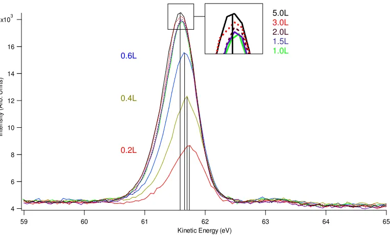
Using the chemical shift in the C 1s photoemission peaks (see fig.4.11) from two inequivalent C atoms for two different species of CO adsorbed on Pt(111), scanned-energy mode PhD was performed at the angles tabulated in Table 4.2 (see fig.4.12). The magnification was set to medium and the pass energy to 10 eV. The PhD scans were measured over a kinetic energy range of 68 eV – 372 eV and consisted of 93 EDC’s, each 28 eV wide and 3 eV apart.
θ φ
0o
Normal Emission
10o 20o 30o 40o 50o
[121]
[110]
[211]
Fig.4.11 C 1s photoemission peaks for two species of CO on Pt(111), atop and bridge labelled A and B respectively.
Energy eV
In
te
ns
ity
(
ar
b.
u
ni
ts
)
1.1
1.0
0.9
0.8
0.7
180 175
170 165
160 155
Fit
Experimental Data B
A
Table.4.2. The polar (θ) and azimuthal (φ) angles at which the PhD scans were measured are indicated by the
When fitting the data, care had to be taken to ensure that chemically equivalent sites were included in the theoretical models. For example, the bridge sites on the Pt(111) surface are chemically equivalent due to the symmetry of the crystal (see fig.4.13). Therefore, if a domain exists in which the CO molecules occupy certain bridge sites, other domains will exist in which the CO molecules occupy the other bridge sites. If there are six equivalent adsorption sites, six domains must be defined and therefore six symmetries must be included. If the number of symmetries included is too few, a false R-factor minimum may be obtained which may in turn suggest a false adsorbate position. Six symmetries were included in the analysis under discussion.
Fig.4.12. The azimuthal directions used in table 4.2; the 0o polar angle is perpendicular to
the page.
[110]
[211] [121]
4.4 Results and Discussion
The results were integrated as detailed in chapter 2, to produce a modulation function for each
direction in which the PhD scans were taken. The modulation functions (figs. 4.14 and 4.15)
were used directly to obtain a general idea of the orientation of the adsorbate with respect to the
substrate. Fig.4.14 shows that the modulation function for (A) shows stronger oscillations when
compared with that for (B) when measured at normal emission. This is indicative of a high
degree of backscattering suggesting that the Pt-C bond, represented by (A) is orientated in the
direction of the analyser and therefore likely to be an atop species.
However, when measured at 40o off normal emission in the [110] direction (see fig.4.15), the
intensity of the modulation function for (A) decreases and that for (B) becomes dominant suggesting that the higher kinetic energy peak represented by (B) corresponds to the bridge species.
Fig.4.14 A corresponds to the modulation function produced from lower KE peak and B, from the higher KE peak. The chi curves are given relative to one another and represent intensity against energy. They have been offset on the y- axis for comparison.
Energy (eV)
In
te
ns
ity
(
ar
b.
u
ni
ts
)
0.00
350 300
250 200
150 100
0.12
-0.12 0.00
0.12
-0.12
A
This method is only qualitative but nevertheless, provides an initial indication of the probable adsorption sites and is consistent with the findings of F. Bondino et al. [40].
Even though all the previous publications point to preferential adsorption of CO at atop and bridge sites, hollow site adsorption was also considered. This was done by placing a single adsorbate on the surface in turn at the ideal atop, bridge, HCP and FCC adsorption positions and comparing the pre optimized R-factors for the low and high kinetic energy spectra (A and B). Table 4.3 shows that when using the low kinetic energy spectra, the atop site is clearly
favoured giving an R-factor of 0.3512 with a var(Rmin) value of 0.0656 which means that any
site giving an R-factor greater than 0.4168 can be excluded. On the other hand, when the high kinetic energy spectra, are used the bridge site is clearly favoured giving an R-factor of 0.3441.
This gives a var(Rmin) value of 0.0704 meaning any site giving an R-factor greater than 0.4143
can be excluded.
Spectra Atop Bridge HCP FCC
A 0.3512 0.8527 0.9344 0.9071
B 0.9080 0.3441 0.9292 0.8945
Once it was established that the PhD data was in agreement with previous studies in terms of preferential adsorption sites and the assignment of the C 1s XPS peaks [40], more
Fig.4.15 A is the chi curve for the lower KE peak at 40o off normal when analyzed in the [110]
direction. B is that for the higher KE peak measured in the same direction. Energy (eV)
In
te
ns
ity
(
ar
b.
u
ni
ts
)
0.00
350 300
250 200
150 100
0.12
-0.12 0.00
0.12
-0.12
A
B
While it has been generally accepted that at a coverage of 0.6 ML, a c(5x√3)rect. overlayer is formed, as highlighted in section 4.1.1, some controversy regarding the actual configuration of this overlayer has persisted. In an effort to settle this controversy, several configurations were analysed with particular attention being given to the following three models. Firstly, the
c(5x√3)rect.-2CO proposed by Petrova et al. [27] (fig.4.16:A) consisting of an atop/bridge ratio
of 1:2; that proposed by Avery [29] with a 2:1 ratio (fig.4.16:B) and finally, the 2:1 atop/bridge configuration proposed by Persson et al. [28] (fig.4.16:C).
The c(5x√3)rect.-3CO proposed by Petrova et al. [27] consisting of a 1:2 atop/bridge ratio finds
little or no support in the literature. However the studies presenting evidence for a 2:1 ratio are not in agreement as to what form this 2:1 overlayer configuration takes. In order for Petrova’s model to be properly eliminated a comprehensive PhD analysis had to be performed. The best achievable R-factors for this configuration were found to be 0.2246 using the atop spectra, 0.3221 using the bridge spectra and 0.2633 using the combined spectra. These R-factors resulted from the structural model shown in fig.4.17.
Fig.4.16 CO/Pt(111) Overlayer configurations proposed in the literature. A consisting of an atop/bridge ratio of 1:2 proposed by Petrova et al. [27]. B and C consisting of atop/bridge ratios of 2:1 proposed by Avery et al. [29] and Persson at al. [28] respectively.
A
Fig. 4.17 Atomic displacement in the xyz directions for the theoretical model deduced from analysing atop and bridge spectra separately for the overlayer proposed by Petrova [27]. The reference lines are black and dashed, the solid red lines represent the carbon displacements, the solid blue lines represent the oxygen displacements and the solid black lines represent the substrate displacements.
0.041Ǻ
0.001Ǻ
0.152Ǻ
0.147Ǻ
0.038Ǻ
0.088Ǻ
0.182Ǻ
0.104Ǻ
0.006Ǻ
1.831Ǻ
1.443Ǻ
2.266Ǻ
2.266Ǻ
1.199Ǻ
1.17Ǻ
[image:49.595.73.523.61.680.2]While this model produces a reasonably good R-factor especially when the weak scattering ability of Pt is considered, a questionable result of this configuration is evident in the C-O bond lengths. The C-O bond length for the atop species is longer than that for the bridge species; 1.233 +0.087/-0.065 Å and 1.181 +0.36/-0.16 Å respectively. Admittedly, the discrepancy is somewhat lost in the variance but such a discrepancy can be an indication that other parameters are incorrect. A hint as to what this might be can be found in the XPS data. The high resolution spectrum shown in fig.4.9 reveals that the intensity of the atop peak appears to be approximately twice that of the bridge peak. Assuming the cro

![Fig. 4.6. The c(√3 x 5)rect.3CO arrangement as proposed by Petrova et al [27] (based on a diagram presented in their paper)](https://thumb-us.123doks.com/thumbv2/123dok_us/378909.1038585/37.595.248.362.364.484/fig-arrangement-proposed-petrova-based-diagram-presented-paper.webp)
![Table 4.1. LEED patterns produced by the LEEDpat2 program for a hexagonal p3m1 2D lattice [38] consistent with that found experimentally for the 0.6 ML CO/Pt(111) adsorption system](https://thumb-us.123doks.com/thumbv2/123dok_us/378909.1038585/43.595.85.529.275.737/patterns-produced-leedpat-program-hexagonal-consistent-experimentally-adsorption.webp)
![Fig. 4.17 Atomic displacement in the xyz directions for the theoretical model deduced from analysing atop and bridge spectra separately for the overlayer proposed by Petrova [27]](https://thumb-us.123doks.com/thumbv2/123dok_us/378909.1038585/49.595.73.523.61.680/displacement-directions-theoretical-analysing-separately-overlayer-proposed-petrova.webp)
![Fig. 4.19 Comparison of strip spacing for the overlayers proposed by Avery [29] and Persson et al](https://thumb-us.123doks.com/thumbv2/123dok_us/378909.1038585/52.595.202.498.372.704/fig-comparison-strip-spacing-overlayers-proposed-avery-persson.webp)
![Fig. 5.6. 20º perspective views along the [001], [110] and [110] directions corresponding to diagrams A, B and C, respectively](https://thumb-us.123doks.com/thumbv2/123dok_us/378909.1038585/70.595.212.399.180.354/fig-o-perspective-views-directions-corresponding-diagrams-respectively.webp)